Fast detection of single-charge tunneling to a graphene quantum dot in a multi-level regime
Abstract
In situ-tunable radio-frequency charge detection is used for the determination of the tunneling rates into and out of a graphene single quantum dot connected to only one lead. An analytical model for calculating these rates in the multi-level tunneling regime is presented and found to correspond very well to our experimental observations.
pacs:
73.23.Hk, 72.80.Vp, 85.35.BeTime-resolved charge detection on quantum dots is a powerful technique to straightforwardly extract single-particle transport properties such as the occupation probability of quantum dots determined by the Fermi distribution function in the leads and the dot-lead tunneling rates schleser:04 ; vandersypen:04 . Recording the charge-detector signal through radio-frequency (rf) reflection measurements schoelkopf:98 can enhance the time resolution drastically, enabling studies of systems with larger tunneling rates.
To date, these types of experiments mainly study quantum dots in the single-level regime, and investigations involving transport through more than one level have focused on the phenomenon of super-Poissonian noise belzig:05 ; gustavsson:06b ; fricke:07 . Here, we present measurements and an analytical calculation of multi-level tunneling rates using a graphene single quantum dot connected to one lead.
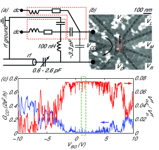
Our charge-detection experiments were performed by incorporating a graphene nanoconstriction charge detector, capacitively coupled to a graphene single quantum dot, into an in situ-tunable resonant circuit mueller:10 . A schematic view of the latter and an atomic force microscopy image of the former are presented in Figs. 1(a) and (b), respectively. The structure was fabricated through reactive ion etching on a mechanically exfoliated graphene flake novoselov:04 . The parts of the graphene flake etched away are emphasized by dashed black lines in Fig. 1(b) to enhance visibility. The roughly 100 nm sized quantum dot (marked by the dashed red ellipse) and the nanoconstriction (designated by the single-sided arrow) can be tuned by in-plane gates and a global backgate. In spite of the symmetric design of the barriers forming the quantum dot, only the upper lead (source; represented by the double-sided arrow) was tunnel-coupled to the dot. Therefore, we were not able to measure direct transport through the graphene quantum dot. A more detailed description of the fabrication procedure for this kind of devices can be found in Ref. guettinger:09 .
Due to the large stray capacitance formed between the metallic bond pads and the highly doped silicon backgate, high-quality rf matching of graphene samples using the standard circuit design forming a resonance between a series inductor and the total stray capacitance is difficult. One way to avoid this challenge is to remove the backgate underneath the bond pads, which however complicates the already involved fabrication of graphene nanostructures. We chose an alternative circuit design consisting of a tunable capacitance in series to a parallel circuit mueller:10 . Doing so and harnessing the large change in conductance of the nanoconstriction upon addition of a single charge to the quantum dot due to the proximity of the structures ( at ) yields a very good charge sensitivity of vink:07 ; reilly:07 ; cassidy:07 ; mueller:10 ; barthel:10 .
All our measurements were performed in a variable-temperature insert at a temperature of roughly 2 K.
The blue curve in Fig. 1(c) shows the dc conductance (left axis) through the nanoconstriction charge sensor as a function of backgate voltage, while the red curve is the simultaneously acquired rf reflection coefficient. Both measurements reveal a transport gap in the backgate range between around and 4 V. Subsequent measurements are performed in the regime of the dashed green box, in proximity of the charge-neutrality point of the graphene charge sensor Note2 .
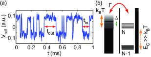
Tuning all gate voltages such that the quantum dot is at a charge-degeneracy point between and negative charges on the dot Note3 and recording the charge-detector conductance via rf reflectometry allows for studying tunneling of single charge carriers in real-time, as shown in Fig. 2(a). This trace has been 8-th order Bessel low-pass filtered at 200 kHz - roughly two orders of magnitude faster than with previous time-resolved experiments on graphene quantum dots guettinger:11 - and sampled at 500 kHz to ensure large enough signal-to-noise ratio for reliable electron counting gustavsson:06 . From the average time a negative charge spends inside (out of) the dot we can compute the dot occupation probability and the rate for tunneling out of (into) the quantum dot.
At our elevated temperatures we have good reason jacobsen:12 to assume that we are in a multi-level tunneling regime - an assumption that we will show to be correct in our discussion of the experimental data. Thus we now calculate the tunneling rates of a quantum dot connected to one lead in the multi-level regime schematized in Fig. 2(b). Our analysis closely follows the work of Beenakker beenakker:91 in which all the ingredients for the subsequent analysis are provided, and we also adopt the notation thereof.
The multi-level regime of Coulomb blockade is characterized by a temperature much larger than the single-level spacing but much smaller than the charging energy
| (1) |
The latter inequality is validated by the fact that we extracted an approximate charging energy of typical for graphene quantum dots of this size (see for instance Ref. guettinger:11 ), whereas we assume the former to be true since we have not observed any sign of excited states in either the similarly sized charge detector or the dot itself. Nevertheless, we shall assert the inequality’s validity later-on.
It has been shown in Ref. beenakker:91 that the rate for tunneling into a quantum dot occupied by charges is given by the sum over all quantum dot states of their respective couplings multiplied by the probability to have a state at energy available in the lead (given by the Fermi distribution function ) and the conditional probability of having state empty in an -fold occupied dot in equilibrium
| (2) | |||||
where is the electrostatic energy of a dot containing negative charge carriers, and is the chemical potential in the lead(s). Beenakker has also elucidated that can be expressed as a Fermi function in the high-temperature limit, where the chemical potential of the dot is determined by
| (3) |
By assuming the couplings to be equal and independent of energy, we can replace the sum by an integral over energy times density of states which we will also assume to be energy-independent. Thus we can perform the integration which yields
| (4) | |||||
where is the energy detuning between the chemical potentials in the lead and the dot (note that our definition of has an additional minus sign compared to the one of Ref. beenakker:91 ). Analogously, we can compute
| (5) | |||||
In this last equality we have made use of the fact that at our relevant energies .
Adding these two expressions leads to the inverse of the correlation time of the random telegraph signal machlup:54 given by
| (6) |
We want to emphasize that in contrast to the above expression, the sum of tunnel rates is constant with respect to detuning in the single-level regime if the couplings for tunneling-in and -out are equal (and are only varying over a range of the order of otherwise). Therefore, a strongly varying sum of tunneling rates excludes a single-level regime.
The expected rate of events (the number of times per second an electron tunnels in and out of the quantum dot) can now be calculated to be
| (7) | |||||
equivalent to what Beenakker found for the conductance through a dot in the multi-level regime (and what Kulik and Shekhter found for transport through granular metals kulik:75 ) since in all instances, tunneling-in and -out are treated on an equal footing.
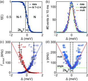
Equipped with these analytical expressions for the tunneling rates, we turn to our experimental results. Figure 3(a) shows the fraction of time the quantum dot is devoid of the -th excess charge when sweeping over the charge-degeneracy point, reflecting the Fermi distribution function of the lead. Fitting the measured data (blue dots) with a Fermi function (solid black curve) results in a temperature of . Using this temperature, we can compare the number of tunneling events extracted from the same time traces with the expected number in a single- (dashed green line; see Ref. beenakker:91 ) and multi-level (solid red line; Eq. 7) regime in Fig. 3(b). We find that the solid red line corresponding to multi-level tunneling matches the measurements better Note4 .
In Fig. 3(c) we show the experimentally extracted rates for tunneling-in (blue circles) and tunneling-out (red crosses). Additionally, we plot the analytical functions for the rates given by Eqs. 4 and 5 as solid lines. The only fit parameter for these curves is the product of tunnel coupling and density of states which was chosen such that the experimental results coincide with the calculations at zero detuning. The error bars indicating the uncertainty of the determination of the tunneling rates from the dwell times gustavsson:06b are only shown for one in 20 data points to enhance visibility. Finally, the sum of these tunneling rates is presented in Fig. 3(d) for both, experiment (blue squares) and single- (dotted green line) as well as multi-level (solid red line; Eq. 6) models. As we observe a linear increase in the sum of the rates for detunings above , we can be certain to be in a multi-level regime.
In all plots of Fig. 3, the horizontal axis has been converted to energy using a lever arm set via the relative influence of the swept backgate and the dot source lead Note1 .
The qualitative and quantitative agreement between our experiments and theoretical calculations is striking, especially considering that only one free parameter is available, since temperature has been fixed by the Fermi fit in (a). Nevertheless, we observe a deviation from the model for large detuning, where the experimentally obtained values lie distinctly above our expectations. This may originate from the fact that, in contrast to our assumptions, either the density of states or the tunnel couplings in the dot are not entirely independent of energy. Furthermore, the couplings may be different for each state . Also, it is conceivable that only a finite number of states contribute to tunneling. From the energy-dependence of the sum of tunneling rates in Fig. 3(d), though, we can definitely exclude single-level tunneling. Missed events due to our large yet finite bandwidth lead to a further enhancement of the numeric value of the measured tunnel rates for large and can therefore not explain the deviations.
In conclusion we have performed time-resolved charge detection measurements on a graphene quantum dot using rf reflectometry with large bandwidth. From these experiments we have extracted the rates for tunneling-in and tunneling-out of the dot, which are in good agreement with our analytical model for multi-level tunneling to a single lead. This type of fast charge detection on graphene quantum dots opens possibilities for studying interactions of Dirac Fermions in the framework of full counting statistics and is a great instrument for determining spin relaxation times in graphene quantum dot circuits.
We thank C. Barengo for invaluable technical assistance and B. Küng and Y. Komijani for fruitful discussions. Funding by the Swiss National Science Foundation (SNF) via National Center of Competence in Research (NCCR) Nanoscale Science is gratefully acknowledged.
References
- (1) R. Schleser, E. Ruh, T. Ihn, K. Ensslin, D. C. Driscoll, and A. C. Gossard, Appl. Phys. Lett. 85, 2005 (2004)
- (2) L. M. K. Vandersypen, J. M. Elzermann, R. N. Schouten, L. H. Willems van Beveren, R. Hanson, and L. P. Kouwenhoven, L. P., Appl. Phys. Lett. 85, 4394 (2004)
- (3) R. J. Schoelkopf, P. Wahlgren, A. A. Kozhenikov, P. Delsing, and D. E. Prober, Science 280, 1238 (1998)
- (4) W. Belzig, Phys. Rev. B 71, 161301(R) (2005)
- (5) S. Gustavsson, R. Leturcq, B. Simovič, R. Schleser, P. Studerus, T. Ihn, K. Ensslin, D. C. Driscoll, and A. C. Gossard, Phys. Rev. B 74, 195305 (2006)
- (6) C. Fricke, F. Hohls, W. Wegscheider, and R. J. Haug, Phys. Rev. B 76, 155307 (2007)
- (7) T. Müller, B. Küng, S. Hellmüller, P. Studerus, K. Ensslin, T. Ihn, M. Reinwald, and W. Wegscheider, Appl. Phys. Lett. 97, 202104 (2010)
- (8) K. Novoselov, A. K. Geim, S. V. Morozov, D. Jiang, Y. Zhanh, S. V. Dubonos, I. V. Grigorieva, A. A. Firsov, Science 306 666 (2004)
- (9) J. Güttinger, C. Stampfer, T. Frey, T. Ihn, and K. Ensslin, Phys. Status Solidi 246, 2553 (2009)
- (10) I. T. Vink, T. Nooitgedagt, R. N. Schouten, L. M. K. Vandersypen, and W. Wegscheider, Appl. Phys. Lett. 91 123512 (2007)
- (11) D. J. Reilly, C. M. Marcus, M. P. Hanson, and A. C. Gossard, Appl. Phys. Lett. 91, 162101 (2007)
- (12) M. C. Cassidy, A. S. Dzurak, R. G. Clark, K. D. Petersson, I. Farrer, D. A. Ritchie, and C. G. Smith, Appl. Phys. Lett. 91, 222104 (2007)
- (13) C. Barthel, M. Kjærgaard, J. Medford, M. Stopa, C. M. Marcus, M. P. Hanson and A. C. Gossard, Phys. Rev. B 87, 161308(R) (2010)
- (14) Since the charge sensor and the quantum dot were fabricated from the same flake it seems fair to assume the Dirac points of both devices to be rather close. Thus, we have chosen settings close to the detector’s charge-neutrality point, where the low density of states should result in small enough tunneling rates.
- (15) From Fig. 1(c) we may expect to be in the hole regime. Nevertheless, we are always refering to single negative charges being added to the dot (removal of a hole) in order to avoid confusion.
- (16) J. Güttinger, J. Seif, C. Stampfer, A. Capelli, K. Ensslin, and T. Ihn, Phys. Rev. B 83, 165445 (2011)
- (17) S. Gustavsson, R. Leturcq, B. Simovič, R. Schleser, T. Ihn, P. Studerus, K. Ensslin, D. C. Driscoll, and A. C. Gossard, Phys. Rev. Lett. 96 076605 (2006)
- (18) A. Jacobsen, P. Simonet, K. Ensslin, and T. Ihn, N. J. Phys. 14 023052 (2012)
- (19) C. W. J. Beenakker, Phys. Rev. B 44, 1646 (1991)
- (20) S. Machlup, J. Appl. Phys. 25, 341 (1954)
- (21) I. O. Kulik and R. I. Shekhter, Sov. Phys. JETP 41, 308 (1975)
- (22) Directly fitting the number of events yields a temperature of for the single-level and for the multi-level regime. The peak height thus extracted was used for the calculated curves.
- (23) This method neglects the capacitive coupling between the source lead and the dot, which may alter the numerical value of the lever arm and thus the extracted temperature. This in turn may stretch or squeeze the graphs with respect to the energy axis but the shape and mutual position of both, experimental and calculated curves will remain unchanged.