Ultra-compact On-Chip Plasmonic Light Concentrator
Ultra-compact on-chip plasmonic light concentration based on a hybrid photonic-plasmonic structure
Ye Luo, Maysamreza Chamanzar and Ali Adibi
School of Electrical and Computer Engineering, Georgia Institute of Technology,
777 Atlantic Drive NW,
Atlanta, GA 30332–0250
luoye@ece.gatech.edu
Abstract
We present a novel approach for achieving tightly concentrated optical field by a hybrid photonic-plasmonic device in an integrated platform, which is a triangle-shaped metal taper mounted on top of a dielectric waveguide. This device, which we call a plasmomic light concentrator (PLC), can achieve side-coupling of light energy from the dielectric waveguide to the plasmonic region and light focusing into the apex of the metal taper(at the scale ) at the same time. For demonstration, we numerically investigate a PLC, which is a metal (Au) taper on a dielectric () waveguide at working wavelengths around . We show that three major effects (mode beat, nanofocusing, and weak resonance) interplay to generate this light concentration phenomenon and govern the performance of the device. By coordinating these effects, the PLC can be designed to be super compact while maintaining high efficiency over a wide band. In particular, we demonstrate that under optimized size parameters and wavelength a field concentration factor (FCF), which is the ratio of the norm of the electric field at the apex over the average norm of the electric field in the inputting waveguide, of about can be achieved with the length of the device less than for a moderate tip radius . Moreover, we show that a FCF of is achievable over a wavelength range when the length of the device is further reduced to about .
OCIS codes: (130.3120) Integrated optics devices;
References and links
- [1] J. A. Schuller, E. S. Barnard, W. Cai, Y. Jun, J. S. White, and M. L. Brongersma, “Plasmonics for extreme light concentration and manipulation,” Nat. Materials 9, 193–204 (2010).
- [2] Z. Liu, J. M. Steele, W. Srituravanich, Y. Pikus, C. Sun, and X. Zhang, “Focusing surface plasmons with a plasmonic lens,” Nano Lett. 5, 1726–1729 (2005).
- [3] W. Chen, D. C. Abeysinghe, R. L. Nelson, and Q. Zhan, “Plasmonic lens made of multiple concentric metallic rings under radially polarized illumination,” Nano Lett. 9 4320–4325 (2009).
- [4] L Yin, V. K. Vlasko-Vlasov, J. Pearson, J. M. Hiller, J. Hua, U. Welp, D. E. Brown, and C. W. Kimball, “Subwavelength Focusing and Guiding of Surface Plasmons,” Nano Lett. 5, 1399–1402 (2005).
- [5] A. Yanai, and U. Levy, “Plasmonic focusing with a coaxial structure illuminated by radially polarized light,” Opt. Express 17, (2009).
- [6] K. V. Nerkararyan, “Superfocusing on a surface polariton in a wedge-like structure,” Phys. Lett. A 237, 103–105 (1997).
- [7] A. J. Babadjanyan, N. L. Margaryan, and K. V. Nerkararyan, “Superfocusing of surface polaritons in the conical structure,” J. Appl. Phys. 87, 3785–3788 (2000).
- [8] M. I. Stockman, “Nanofocusing of optical energy in tapered plasmonic waveguides,” Phys. Rev. Lett. 93, 137404 (2004).
- [9] K. C. Vernon, D. K. Gramotnev, and D. F. P. Pile, “Adiabatic nanofocusing of plasmons by a sharp metal wedge on a dielectric substrate,” J. Appl. Phys. 101, 104312 (2007).
- [10] E. Moreno, S. G. Rodrigo, S. I. Bozhevolnyi, L. Martín-Moreno, and F. J. García-Vidal, “Guiding and focusing of electromagnetic fields with wedge plasmon polaritons,” Phys. Rev. Lett. 100, 023901 (2008).
- [11] S. I. Bozhevolnyi, and K. V. Nerkararyan, “Adiabatic nanofocusing of channel plasmon polaritons,” Opt. Lett. 35, 541–543 (2009).
- [12] V. S. Volkov, S. I. Bozhevolnyi, S. G. Rodrigo, L. Martín-Moreno, F. J. García-Vidal, E. Devaux, and T. W. Ebbesen, “Nanofocusing with Channel Plasmon Polaritons,” Nano Lett. 9, 1278–1282 (2009).
- [13] V. S. Volkov, J. Gosciniak, S. I. Bozhevolnyi, S. G. Rodrigo, L. Martín-Moreno, F. J. García-Vidal, E. Devaux, and T. W. Ebbesen, “Plasmonic candle: towards efficient nanofocusing with channel plasmon polaritons,” New J. Phys. 11, 113043 (2009).
- [14] Z. Fang, H. Qi, C. Wang, X. Zhu, “Hybrid Plasmonic Waveguide Based on Tapered Dielectric Nanoribbon: Excitation and Focusing,” Plasmonics 5, 201–212 (2010).
- [15] K. Tanaka, K. Katayama, and M. Tanaka, “Nanofocusing of surface plasmon polaritons by a pyramidal structure on an aperture,” Opt. Express 18, (2010).
- [16] N. C. Lindquist, P. Nagpal, A. Lesuffleur, D. J. Norris, and S. Oh, “Three-dimensional plasmonic nanofocusing,” Nano Lett. 10, 1369–1373 (2010).
- [17] C. Ropers, C. C. Neacsu, T. Elsaesser, M. Albrecht, M. B. Raschke, and C. Lienau, “Grating-coupling of surface plasmons onto metallic tips: A nanoconfined light source,” Nano Lett. 7, 2784–2788 (2007).
- [18] E. Verhagen, A. Polman, and L. Kuipers, “Nanofocusing in laterally tapered plasmonic waveguides,” Opt. Express 16, 766–788 (2008).
- [19] A. Normatov, P. Ginzburg1, N. Berkovitch, G. M. Lerman, A. Yanai, U. Levy and M. Orenstein, “Efficient coupling and field enhancement for the nano-scale: plasmonic needle,” Opt. Express 18, (2009).
- [20] H. Choi, D. F. P. Pile, S. Nam, G. Bartal, and X. Zhang, “Compressing surface plasmons for nano-scale optical focusing,” Opt. Express 17, 7519–7524 (2009).
- [21] M. Schnell, P. Alonso-González, L. Arzubiaga, F. Casanova, L. E. Hueso, A. Chuvilin, and R. Hillenbrand, “Nanofocusing of mid-infrared energy with tapered transmission lines,” Nature Photonics 5, 283–287 (2011).
- [22] R. Yang, R. A. Wahsheh, Z. Lu, and M. A. G. Abushagur, “Efficiently squeezing near infrared light into a -by- nanospot,” Opt. Express Opt. Express 16, 20142 (2008).
- [23] B. Desiatov, I. Goykhman and U. Levy, “On-chip focusing of light by metallic nanotip,” Frontiers in Optics, OSA Technical Digest (CD) (OSA, 2010), paper FThB7.
- [24] B. Desiatov, I. Goykhman and U. Levy, “Nanoscale mode selector in silicon waveguide for on-chip nanofocusing applications,” Nano Letters 9, 3381–3386 (2009).
- [25] B. Desiatov, I. Goykhman and U. Levy, “Plasmonic nanofocusing of light in an integrated silicon photonics platform,” Opt. Express 19, 13150–13157 (2011).
- [26] Y. Luo, M. Chamanzar, A. A. Eftekhar, and A. Adibi, “On-chip Nanofocusing Using a Hybrid Plasmonic-Dieletric Tapered Waveguide,” Integrated Photonics Research, Silicon and Nanophotonics, OSA Technical Digest (CD) (OSA, 2011), paper ITuD7.
- [27] X. He, L, Yang, and T. Yang, “Optical nanofocusing by tapering coupled photonic-plasmonic waveguides,” Opt. Express 19, 12865–12872 (2011).
- [28] P. Berini, “Plasmon-polariton waves guided by thin lossy metal films of finite width Bound modes of symmetric structures,” Phys. Rev. B 61, 10484–10503 (2000).
- [29] P. Berini, “Plasmon-polariton waves guided by thin lossy metal films of finite width Bound modes of asymmetric structures,” Phys. Rev. B 63, 125417 (2001).
- [30] R. Charbonneau, P. Berini, E. Berolo and E. Lisicka-Shrzek, “Experimental observation of plasmon-polariton waves supported by a thin metal film of finite width,” Opt. Lett. 25, 844–846 (2000).
- [31] J. Park, K. Kim, I. Lee, H. Na, S. Lee, and B. Lee, “Trapping light in plasmonic waveguides,” Opt. Express 18, (2010).
- [32] I. Goykhman, B. Desiatov, and U. Levy, “Experimental demonstration of locally oxidized hybrid silicon-plasmonic waveguide,” Appl. Phys. Lett. 97, (2010).
- [33] D. Dai, and S. He, “Low-loss hybrid plasmonic waveguide with double low-index nano-slots,” Opt. Express 18, (2010).
1 Introduction
Plasmonic metallic structures are well-known for the ability of breaking the diffraction limit and achieving large field enhancements or field confinements in small volumes[1]. One mainstream of the approaches is to focus surface plasmon polariton (SPP) modes, which can be further divided into two categories. One is interference-induced plasmonic nanofocusing. For this type of techniques, the plasmonic excitation sites on a metal film are carefully tuned so that the propogation of SPP originated at the sites can get focused into a hot spot on the metal film. Typical planar patterns for plasmonic excitation on the metal film include individual circular rings [2], multiple concentric rings [3], curved arrays of nanoholes [4], and certain coaxial structures [5]. The other is geometry-induced plasmonic nanofocusing. In principle, tapering the cross section of the SPP propagation gradually will increase the intensity of the SPP and the slow down its group velocity. At the tip end of the taper, the group velocity becomes infinity which means the surface plasmon becomes localized and the energy is highly concentrated [6, 7, 8, 9, 10, 11, 12, 13, 14, 15, 16, 17, 18, 19, 20, 21]. This type of techniques can accurately control the focus point and usually with a higher concentrating ability.
Conventionally, the nanofocusing techniques have the SPP excited from free space and the devices are usually bulky. There are two issues which limit the concentration efficiency. First, the efficiency of SPP excitation is usually low and unstable. Second, the SPP propagation length is limited by the lossy nature of metal. Very recently, several approaches of realizing plasmonic nanofocusing on integrated-optics platforms have been reported [22, 23, 24, 25, 26, 27]. Using these on-chip light concentration techniques, the light energy is coupled from a photonic waveguide to a plasmonic structure (usually a metallic taper) and then concentrating the light energy to the tip of the taper. The coupling from the photonic waveguide to the plasmonic structure is efficient and robust, while the plasmonic part is usually compact since it only concentrates light energy from a “” scale to a “” scale. Therefore, the two limitations for free space plasmonic nanofocusing can be well addressed by the on-chip techniques. However, instead of demonstrating the promising plasmonic concentration phenomena, these reports lack a systematic analysis of the underlying mechanisms that governing the performance of the devices.
In this paper, we will present the design of a novel ultra-compact on-chip plasmonic light concentrator (PLC), and show that there are three major effects (mode beat, nanofocusing, and weak resonance) that govern this light concentration phenomenon and affect the efficiency of the device. By coordinating these effects, this proposed structure can maintain very high concentrating efficiency while the size dimensions (width length) are the smallest among the all the plasmonic-light-concentration techniques that have been reported.
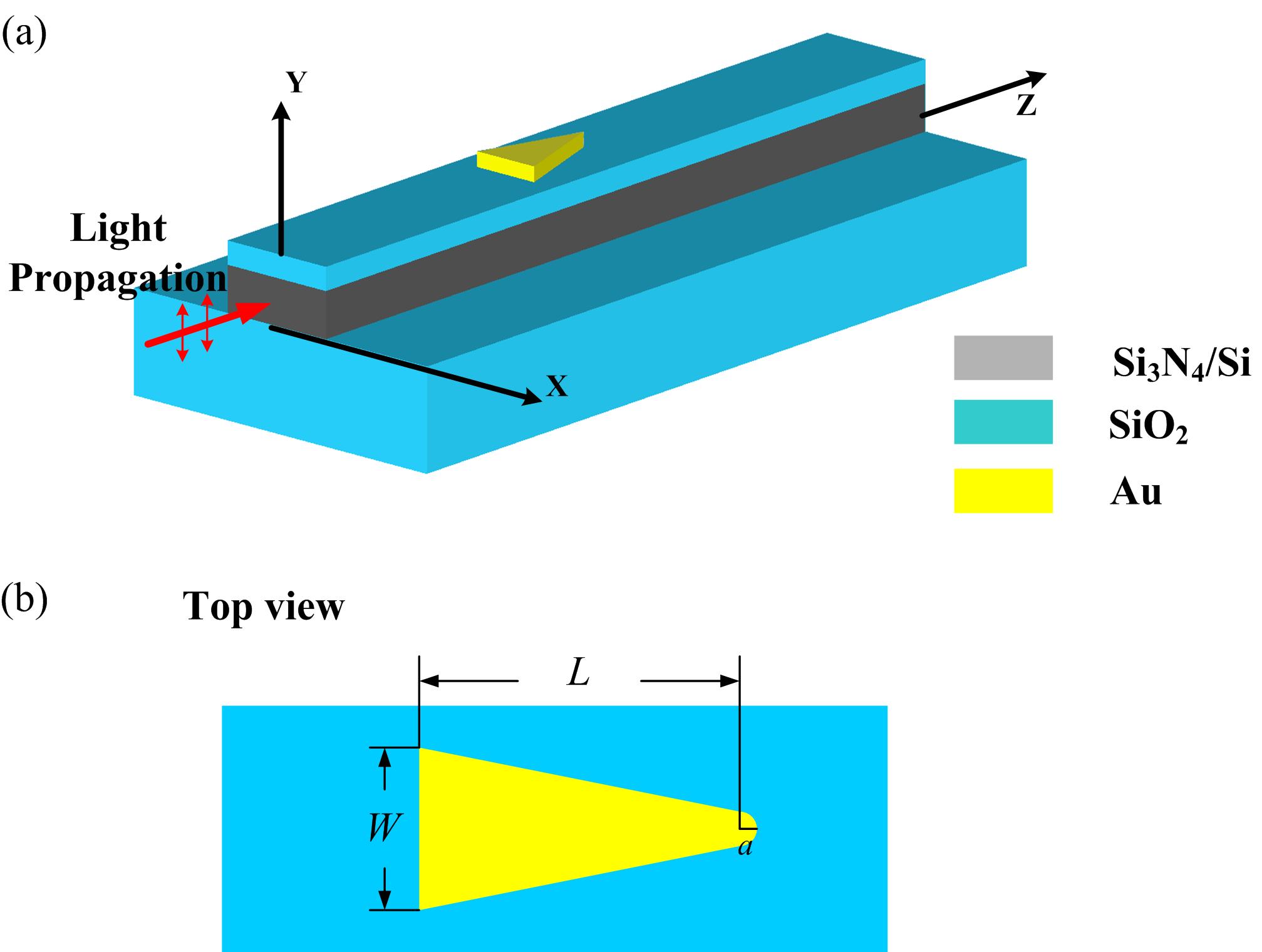
The basic structure of the device is a small triangle-shaped metal taper on top of a dielectric waveguide, as shown in Figure 1(a). In our analysis of this structure, the material for the metal triangle is gold (Au), and the material for the dielectric ridge waveguide is silicon nitride (). The substrate is silicon dioxide (). In addition, a buffer layer is used to separate the metal triangle and the dielectric ridge waveguide. The ambient material is water. The dimensions of the ridge waveguide are chosen to support only the fundamental TM-like (vertical polarization) mode and the fundamental TE-like (horizontal polarization) mode. Only the fundamental TM-like mode can be used to generate light concentration. We set up the coordinate system with -axis in the horizontal direction, -axis in the vertical direction and -axis in the propagation direction of the input light.
Figure 1(b) shows the top view of the metal triangle, which is isosceles. We use to denote the length of the base of the isosceles triangle, and to denote the the length of a perpendicular from the center of the curved tip to the middle point of the base side. In particular, we will call the width of the triangle and the length of the triangle throughout this paper. Since the apex of the metal triangle is always rounded up in real fabrications, we introduce the radius of curvature at the tip as a parameter.
2 Mode analysis of the hybrid photonic-plasmonic waveguide
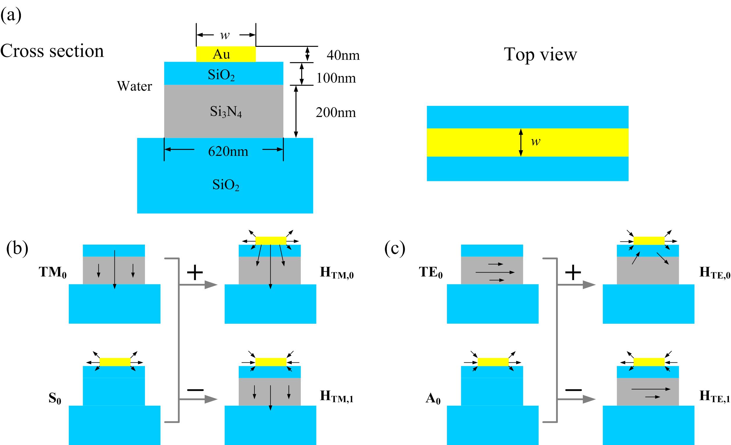
To analyze the behavior of the PLC, we first do mode analysis on a hybrid photonic-plamsmonic waveguide, which is a metal strip on top of a dielectric ridge waveguide with a buffer layer. (There have been reported hybrid photonic-plamsmonic waveguides with different geometric settings. See [28, 29, 30, 31, 32, 33].) As shown in Figure 2(a), the ridge waveguide has dimensions of in width and in thickness. The thickness of the buffer layer is . The Au strip has thickness of and width of . The ambient material is water. Assume the working wavelength is . At this wavelength, the refractive index of is assumed to be , the refractive index of is assumed to be , the refractive index of water is assumed to be , and the permittivity of Au is assumed to be .
Here we study the supermodes in the hybrid waveguides by looking at possible mode couplings between the modes in the corresponding purely photonic waveguide (with no Au layer) and the modes in the corresponding purely plasmonic waveguide (having changed to ). Under the aforementioned dimensions, the purely photonic waveguide only support the fundamental TM-like mode (denoted by ) and the fundamental TE-like mode (denoted by ). The mode can only couple with symmetric modes of the purely plasmonic waveguide, and the mode can only couple with the asymmetric modes of the purely plasmonic waveguide. We only consider the fundamental symmetric () and asymmetric () modes of the purely plasmonic waveguide, since higher order modes are cut off with the dimensions of our structure at the wavelength of . Figure 2(b) shows two supermodes, and , are derived from the superposition of the mode and the mode. The electric field lines are sketched for these modes. Analogously, Figure 2(c) shows two supermodes, and , are derived from the superposition of the mode and the mode.
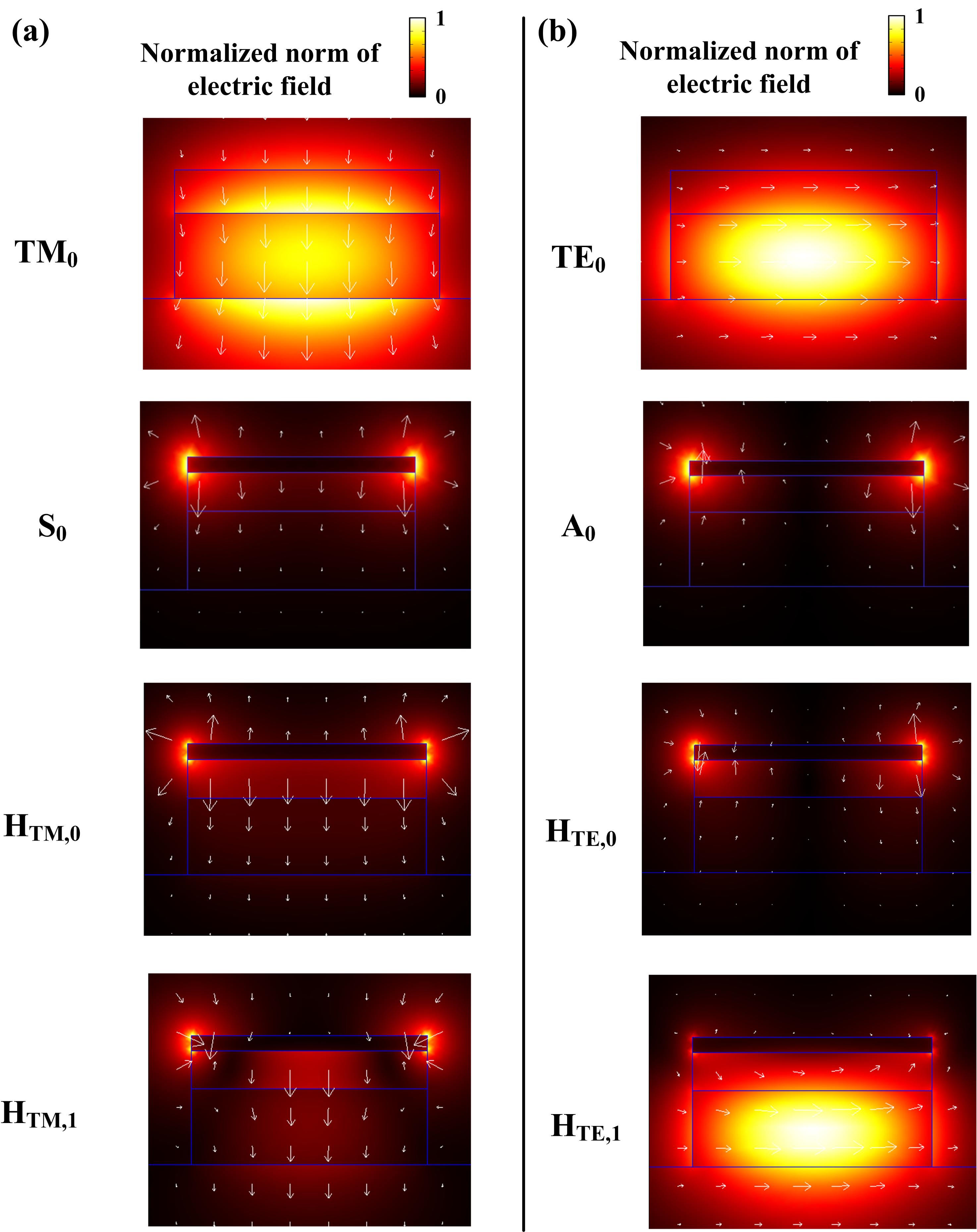
To give more details about the mode-coupling processes, we use finite element method (FEM, COMSOL Multiphysics) to compute the eigenmodes at the wavelength of . Note that the effective indices of the propagating modes must have real parts greater than , which is the refractive index of the substrate.
Figure 3(a) shows the normalized electric field profiles of , , and modes, with the width of the Au strip set to . The electric field lines are plotted. This corresponds to the mode coupling process explained in Figure 2(b). The mode has an effective index of , the mode has an effective index of , the mode has an effective index of , and the mode has an effective index of . Analogously, the related modes in Figure 2(c), , , and , are illustrated in Figure 3(b). The mode has an effective index of , the mode has an effective index of , the mode has an effective index of , and the mode has an effective index of .
The dispersions of the four propagating supermodes (, , and ) are plotted in Figure 4 as the real and imaginary parts of the effective index versus the width of the Au strip. The coordinate “” has minimum , which is the refractive index of the substrate. As we have mentioned, the real part of the effective index of a propagating mode must be greater than . The imaginary part of the effective index accounts for the propagation loss.
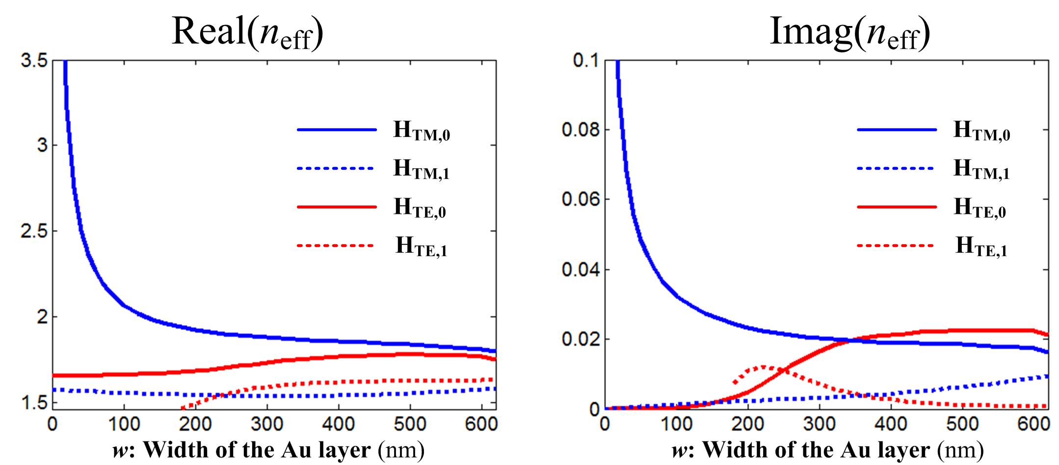
The of is greater than the of , and as decreases, the difference becomes larger. The imaginary parts follow the same trend. This is because as decreases, the light energy becomes more concentrated in the lossy metal region for , while the light energy becomes more concentrated in the dielectric region for . The mode profiles of both supermodes are illustrated in Figure 5 for . As approaches , both the real and imaginary parts of the effective index of goes to infinity, which means that the phase velocity goes to and becomes more and more like a localized mode. When , there is no metal strip and the mode is actually the purely photonic mode . Note that as the width of the metal layer continuously and gradually shrinks down, the amplitude of the mode increases since its propagating velocity slows down. Such a process is common to most geometry-induced plasmonic nanofocusing techniques, and is one of the main mechanisms to generate light concentration in our triangle-shaped plasmonic device. Analogously, we observe that the mode evolves into the purely photonic mode as approaches . Moreover, when , the mode is cut off. Therefore we can not take use of the supermodes and for our application of light concentration.

The supermodes in the hybrid waveguide can be excited by the modes in the corresponding bare (or purely photonic) waveguide. More specifically, the incident mode in the bare waveguide can excite two supermodes ( and ) of the hybrid waveguide. The superposition of these two supermodes at the input end has field in the dielectric region to match the incident mode. Since they have different effective indices, as can be seen from the dispersion diagram in Figure 4, the two supermodes undergo a beat effect with light energy bouncing back and forth between the dielectric region and the metal region. For a specific width of the Au strip, we have
| (1) |
where is the beat length. In particular, at a distance about half the beat length from the input end, the light energy is side-coupled efficiently into the metal region.
3 A PLC with specific size parameters
The PLC presented in this paper can be considered as a taper of the metal strip of the hybrid waveguide introduced in the previous section. The performance of a PLC depends on the interplay of three effects: mode beat, nanofocusing and weak resonance. More specifically, the mode beat effect comes from the interference of the two excited supermodes ( and ), the nanofocusing effect comes from the triangle taper, and the weak resonance effect comes from the reflections at the input end and the apex of the taper. In addition, we may design the device to be ultra-compact while maintaining high efficiency under a wide-band operation. We will demonstrate these effects by analyzing the following device with specific size parameters.
For the dielectric part, we use the same size parameters as in the previous section, i.e., the ridge of width and thickness , and the buffer of width and thickness . The thickness of the Au triangle is . The ambient material is also water. The coordinate system is set up as in Figure 1. In particular, the coordinate origin is chosen such that the plane cuts through the middle of the ridge vertically, the plane coincides with the boundary between the layer and the substrate, and the plane goes through the center of the curved tip.

As shown in Figure 6, we compute the electric field patterns in the horizontal ( in (a) and (b)) and vertical planes ( in (c)) using a D FEM simulation (COMSOL Multiphysics). Here , which is the sum of the thickness of the layer, the thickness of the buffer layer and half of the thickness of the Au layer. The Au triangle has dimensions of , and . We let be the average norm of the incident electric field in the region, which is calculated from the the mode of corresponding purely photonic waveguide. We estimate the total power flow by a plane-wave approximation with the electric field homogeneously distributed and restricted within the region. In particular, the norm of can be computed by the formula
| (2) |
Here is the wave impedance of free space, is the refractive index of , is the area of the cross section of the slab, and is the time-averaged power flow through a cross-section plane . The electric field patterns shown in Figure 6 are normalized to . The light field becomes highly concentrated at the metallic tip. To evaluate the efficiency of field concentration induced by the PLC, we introduce a field concentration factor (FCF) as the normalized electric field norm at the apex point (point in Figure 6 (b) and (c)) in the horizontal plane cutting through the Au layer. In particular, the FCF is in this case. Note that the FCF depends on the radius of curvature . While reducing can afford higher FCF, we should choose large enough for a good estimation on real fabrications. Here we set , and write . (Many authors [25, 27] use the intensity ratio for the factor, which corresponds to the square of the FCF in this paper. Even using a much larger tip radius , our result of the efficiency of light concentration is twofold better than the results that have been reported in literature when evaluated by intensity ratio.)
4 The three underlying effects of the device
As mentioned above, the field concentration is governed by three effects: mode beat, nanofocusing and weak resonance. We have analyzed in Section 2 that the incident mode in the bare photonic waveguide can excite two supermodes, and , in the corresponding hybrid waveguide with a metal (Au) strip integrated on top. The triangle-shaped PLC can be considered as a taper with the width of the Au strip gradually going down to . Therefore, we can still use the two supermodes for the Au taper in our analysis. The mode beat between the two supermodes can make a side-coupling which transfers light energy quickly from the dielectric region to the metal region, and the triangle taper performs plasmonic nanofocusing at the same time. A big advantage of our design is that light coupling (induced by mode beat) and focusing are realized in a single triangle-shaped metal taper so that the device can be made ultra-compact. Note that a short taper also means that we cannot separate the processes of supermode excitation, evolution, interference, and coupling between each other. In the following, we will use a simplified model, in which the two supermodes have constant mode effective indices calculated based on the average width of the taper and the exact ratio change of the two supermodes along the taper is not considered. A certain amount of the light energy will be reflected at the apex and the input end of the taper, and some resonance effect can be observed. This weak resonance also affects the efficiency of how much energy we can concentrate into the tip. By adjusting the size parameters of the Au taper, we can coordinate the three effects and optimize the efficiency of the PLC.
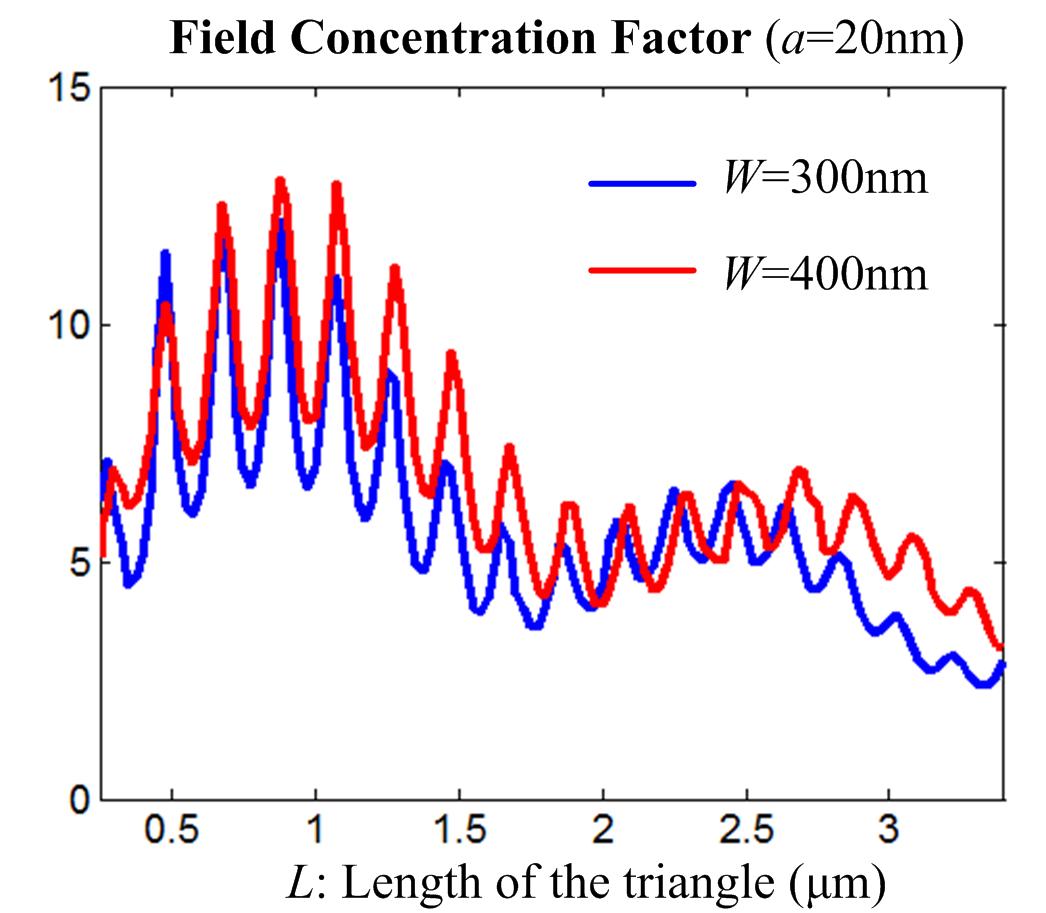
Figure 7 shows how the FCF varies with respect to the length of the Au triangle, while the radius of curvature is always set to be . The wavelength is . The blue curve is for , and the red curve if for . These curves are composed of two oscillatory parts, the slow variations corresponding to the mode-beat effect and the ripples of high oscillation frequency corresponding to the resonance effect. Both of them can be clearly seen from the figure.
Recall that for a hybrid waveguide, we use Equation (1) to estimate the beat length. For the triangle-shaped structure, we may still use Equation (1) for beat-length estimation while is set to be which is about the average width of the triangle. For the blue curve, we have and . Therefore, the real part of is , and of is from Figure 4. By Equation (1), we have
Analyzing analogously on the case (the red curve), we get , , , and
. Note that the beat length for the case is a little bit larger than the beat length of the case. The beat lengths can also be estimated from the figure by approximately locating the the first minimums of slow variation parts. These two methods of beat-length estimations agree with each other very well. When is about half of the beat length, the light energy transfers from the dielectric region to the metal region most efficiently, which results in a higher FCF, as can be seen from the figure. This is actually a principle of design. More accurately speaking, the tapering also induces energy coupling between the two supermodes. In other words, the ratio of energy stored in the two modes will change at different locations along the metal taper, and only the mode becomes localized as the metallic tip.
The ripples on the curves come from the resonance effect. Although the presented structure is not designed based on resonance, the limited length of the taper results in the resonance effect as shown in Figure 7. To calculate the free spectral range (FSR), we need to use the effective index of the mode. The formula is
| (3) |
For example, in the case of , we have , , and . This corresponds to about peaks for the red curve, a good matching with an actual counting on the figure. The FCF is usually the highest, when is chosen to be at a resonance peak close to half the beat length. However, we may reduce to make the PLC supercompact, while still get a high FCF. For example, the FCF is still larger than with for both curves.
5 Analysis of the transmission, reflection and FCF spectra
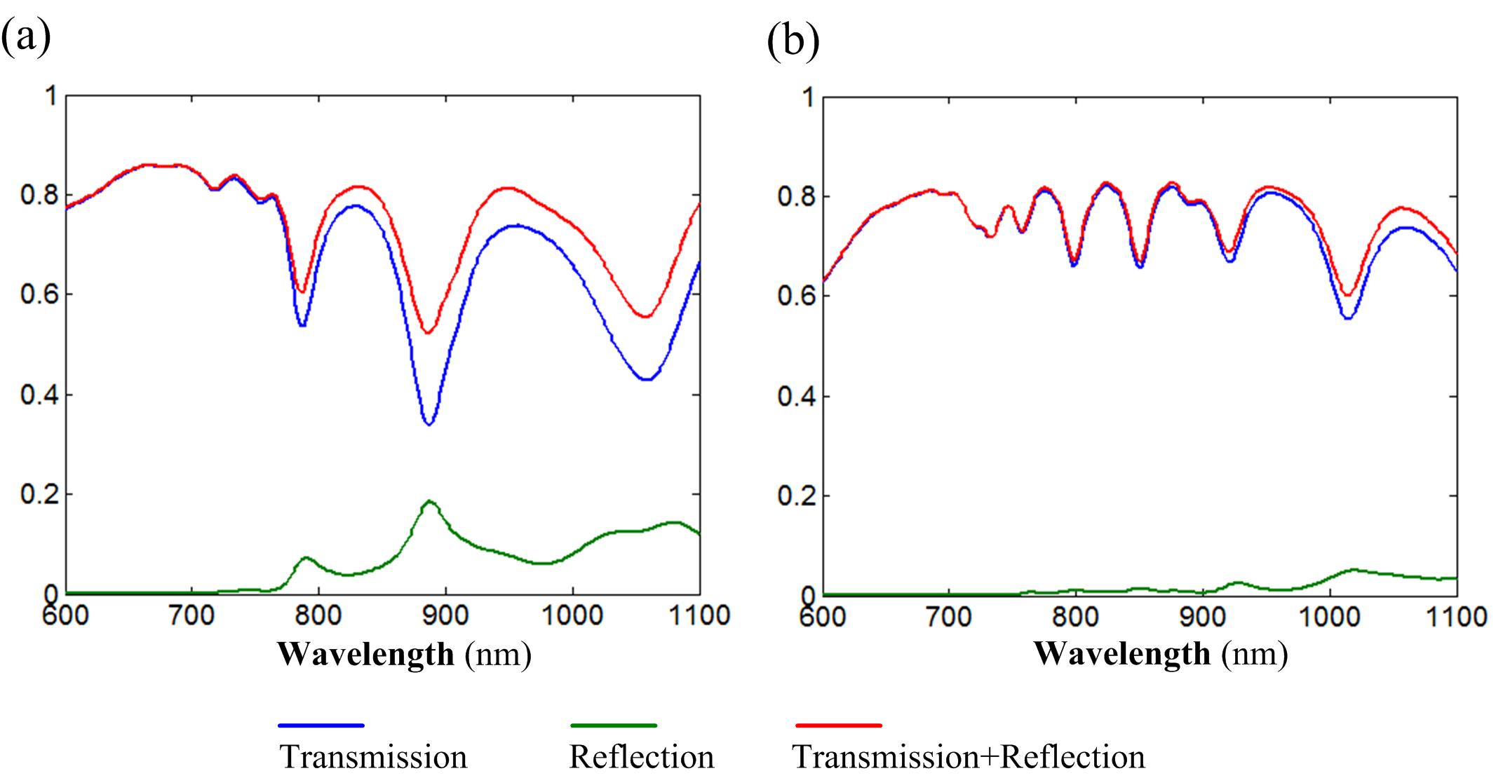
To analyze the transmission spectra, we use the finite-difference-time-domain (FDTD, Lumerical Solutions) method for simulations. Figure 8 shows the transmission, reflection and transmission+reflection spectra for (a) and (b) . We have and . The wavelength range is . Note that the bare waveguide supports higher order TM modes when the wavelength is less than .
Let us consider the case first. As we have computed, when , the beat length is about at the wavelength of . For wavelengths in a range around , we may assume the beat length is stable. Therefore, is around half the beat length, when the PLC is expected to be most efficient. Let the transmission be , and the reflection be . Then indicates the power consumption on the metal structure due to the internal material loss and the radiative loss. As shown in Figure 8(a), the resonance corresponds to the drops in the transmission spectrum and peaks in the reflection spectrum. At resonance, the field is more concentrated in the metal region, which lowers down the transmission but causes a larger reflection. It is noticeable that the reflection part contributes less significantly to the overall than the transmission part, and therefore the profile of the spectrum is basically determined by the transmission spectrum. When the structure is off resonance, we have about , which means a certain amount of power is still coupled into the the metal region. This is quite different from a typical spectrum of a (plasmonic) resonator, which can reach a value very close to when the structure is off resonance. Figure 8(b) shows the spectra in the case. The spacing between two successive drops in the transmission spectrum is clearly less than that of the case. Moreover, since is close to the beat length, the PLC is expected to be less efficient. As a result, the overall reflection is a lot smaller than in the case.
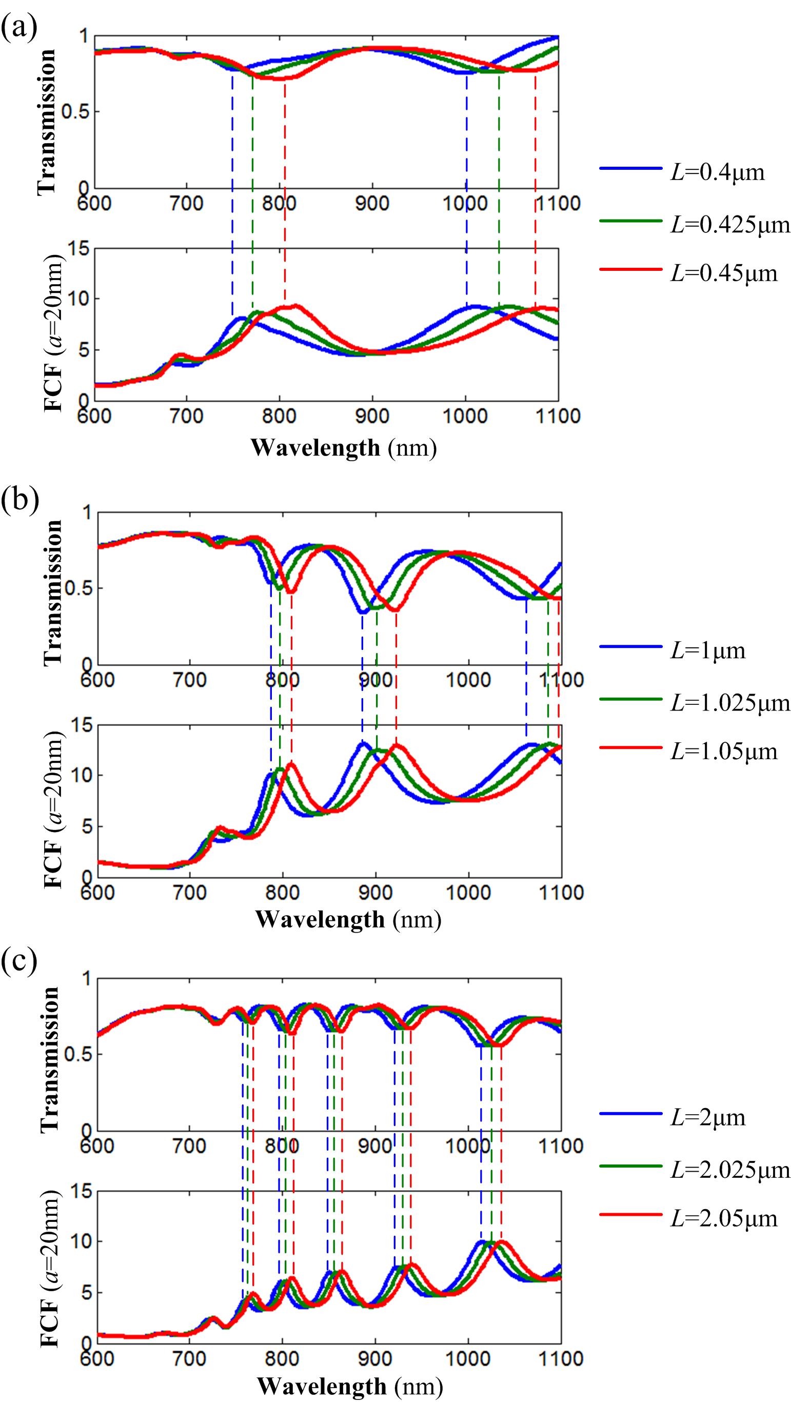
In Figure 9, we make comparisons between transmission spectra and FCF spectra for three groups of metal triangle lengths. The first group (Figure 9(a)) has lengths , and , the second group (Figure 9(b)) has lengths , and , and the third group (Figure 9(c)) has lengths , and . We still have and . Recall that by definition, the FCF() is the normalized norm of the electric field at the point in our coordinate system. When the wavelength is less than , the bare photonic waveguide supports higher order TM modes and the hybrid structure supports more modes other than and . Our analytic model using two supermodes is no longer valid in this case. As a result, the field concentration effect is tremendously suppressed. For wavelengths larger than , the vertical dashed lines indicate that a local minima of the transmission corresponds almost exactly to a local maxima of the FCF, which means that the plasmonic structure is at resonance. Note that when is small, the resonance wavelengths are more sensitive to a change of .
6 Conclusion
In this paper, we have systematically analyzed the behavior and performance of an ultra-compact plasmonic light concentrator (PLC) which is a triangle-shaped Au taper integrated on a waveguide. We use the fundamental TM-like mode for the incident light as an excitation of two supermodes in the hybrid structure. We have showed that three major effects (mode beat, nanofocusing, and weak resonance) interplay to generate the light concentration phenomenon and govern the performance of the device. The principles of design follow by adequately coordinating these effects. The PLC has highest efficiency when length of the triangle is about half the beat length. In particular, we have demonstrated that after an optimization of the size parameters, a field concentration factor (FCF, defined as the norm of the electric field at the apex normalized to the average norm of the electric field in the inputting waveguide) of about can be achieved with the length of the device less than for a moderate tip radius . This is about twice better than those being reported in literature with a much larger device size and an assumption of smaller tip radii. In addition, the dimension of the device can be reduced further (a FCF of is achievable with the length of triangle about ) when necessary.
Moreover, we point out two more advantages of our device. First, our plasmonic device is mounted on top of a photonic waveguide and the waveguide does not terminate after the light concentration as in typical schemes having been reported in literature [22, 23, 25, 27]. This makes our device not only simpler in fabrication, but also perfect to fit into the integrated optical circuit and be combined with other units to make a composite components. Second, the three major effects are actually very common and we can use the same philosophy of design for different materials working at different wavelengths.
Acknowledgement
The authors would like to thank Ali A. Eftekhar for helpful discussions.