Present address: ] Department Materials Science and Engineering, University of Wisconsin-Madison, Madison, WI 53706-1595, USA
Localized state and charge transfer in nitrogen-doped graphene
Abstract
Nitrogen-doped epitaxial graphene grown on SiC(0001̄) was prepared by exposing the surface to an atomic nitrogen flux. Using Scanning Tunneling Microscopy (STM) and Spectroscopy (STS), supported by Density Functional Theory (DFT) calculations, the simple substitution of carbon by nitrogen atoms has been identified as the most common doping configuration. High-resolution images reveal a reduction of local charge density on top of the nitrogen atoms, indicating a charge transfer to the neighboring carbon atoms. For the first time, local STS spectra clearly evidenced the energy levels associated with the chemical doping by nitrogen, localized in the conduction band. Various other nitrogen-related defects have been observed. The bias dependence of their topographic signatures demonstrates the presence of structural configurations more complex than substitution as well as hole-doping.
Graphene has been proposed as a promising alternative to silicon-based electronics for some applications. However a reliable control of its electronic properties, for example by chemical doping, is still a challenging task Castro Neto et al. (2009); Liu et al. (2011); Fuhrer et al. (2010). For carbon-based materials, the incorporation of nitrogen in the lattice is a natural choice because of its ability to form covalent bonds and to modify the electronic properties of sp2 carbon locally, with minor structural perturbations Ewels and Glerup (2005); Lherbier et al. (2008); Zheng et al. (2010). N-doped graphene also offers interesting prospects for various other applications including biosensing Wang et al. (2010), field emission Soin et al. (2011), lithium incorporation Reddy et al. (2010); Cho et al. (2011) or transparent electrodes Kasry et al. (2010).
The substitution of some carbon atoms by nitrogen is expected to give rise to donor states and then to n-type doping Zheng et al. (2010); Wei et al. (2009). The synthesis of chemically modified graphene has been achieved either by direct growth of modified layers Zhao et al. (2011); Panchakarla et al. (2009); Wei et al. (2009); Meyer et al. (2011) or by post-growth treatment of pristine graphene Guo et al. (2010); Lin et al. (2010); Jeong et al. (2011); Wang et al. (2010); Soin et al. (2011). These studies revealed the presence of several atomic configurations for the nitrogen atoms: substitutional (‘graphitic’), pyridine-like, or pyrrole-like N Soin et al. (2011).
However, a clear correlation between the synthesis methods and the atomic configuration of the chemically modified graphene, on the one hand, and between the atomic configuration and the electronic properties, on the other hand, remains a challenging task. A step in this direction has been achieved very recently by Zhao et al. Zhao et al. (2011) through Scanning Tunneling Microscopy (STM) and Spectroscopy (STS) investigations of nitrogen-doped graphene prepared by chemical vapor deposition on a copper substrate with NH3 gas in the feedstock. These authors determined the atomic configuration of the nitrogen atoms to be predominantly (90%) a simple substitution (“graphitic” nitrogen), with the majority of dopants located on the same carbon sublattice of graphene. This work left open some key questions relative to the interpretation of the experimental data. For instance, simulated STM images exhibit a depletion above the N atom (see also Zheng et al. Zheng et al. (2010)) whereas experimental results have no such central feature. More importantly, the N-induced donor energy level has not been evidenced in their STS measurements.
We present here a STM/STS study of N-doped graphene samples on SiC(0001̄) obtained by post-synthesis treatment. Our STM images provide clear evidence of the presence of substitutional nitrogen atoms together with more complex structures presenting well-defined topographical features. Local spectroscopy, supported by simulations based on Density Functional Theory (DFT), reveals for the first time a localized donor state in the electronic density of states related to the substitutional nitrogen atoms. Based on STM images at different biases, we also observed and analysed a change in the STM topographic image with respect to the tip-graphene distance that reconciles experiment and simulation. Doping configurations different from substitution are also analyzed.
Our graphene samples were prepared from C-terminated n-type 6H-SiC(0001̄) wafers, following procedures available in the literature Forbeaux et al. (1999); de Heer et al. (2007); Varchon et al. (2008); Hiebel et al. (2008); Starke and Riedl (2009) which lead to multilayered graphene with misoriented, decoupled layers111See Supplemental Material at […] and references 1-9 therein for details on the sample preparation and on the sample properties.. N-doping was achieved by exposure to an atomic nitrogen flux produced by a remote radiofrequency plasma source fed with N2. The samples were then analyzed using a LT-STM working under UHV conditions (see Supplemental Material and reference 11 therein). In our experimental set-up, the plasma generator is not in the close vicinity of the sample, so that only N radicals (N*) with thermal energy (and no accelerating voltage) interact with graphene. Thus, only the topmost layer is affected by the plasma treatment. This post-synthesis doping method has the advantage over direct growth of modified layers that a well-defined domain could be doped, other part of the sample being kept pristine.

Fig. 1 presents the graphene surface before (a) and after (b) N* exposure. A defect-free honeycomb lattice with an interatomic distance of 1.4 Å is observed for the pristine graphene. After N treatment, many localized features appear as bright dots on the images, demonstrating the effect of the exposure to nitrogen radicals. Moreover, Auger Electron Spectroscopy (AES) confirms that the defects are related to nitrogen doping sites (no other chemical species (e.g. oxygen) are detected in AES) while Raman spectroscopy confirms the presence of defects sites after surface treatment (see Supplemental Material and reference 10 therein). By visual inspection of the STM images, a defect concentration ranging from 0.5% to 1.1% is deduced, depending on the exposure time (0.6% for the figures of the present paper).
A closer look at Fig. 1 (b) reveals that different doping configurations are present. Approximately 75% of them display a triangular shape consisting in a bright spot (approximately 0.4 nm wide) with a three-fold symmetry (inset of Fig. 1 (b)). These images are very similar to the one presented in ref Zhao et al., 2011 and are assigned to substitutional N atoms. No preferential orientation of the trigonal pattern is observed and, consequently, both sublattices of the graphene are affected by the N treatment. The graphene honeycomb pattern remains also unaltered outside of the vicinity of the defect, demonstrating a very local perturbation of the graphene layer. Other typical high resolution images of this defect are shown in Fig. 2 (a-e) for biases ranging from V=-0.4 to +0.5 (see Supplemental Material for a more complete overview). We also systematically observe that the corrugation at the doping site is more pronounced at positive biases, as compared to images recorded at negative biases. At this stage, the doping of graphene with N atoms can then be associated to spatially localized electronic states in the conduction band.
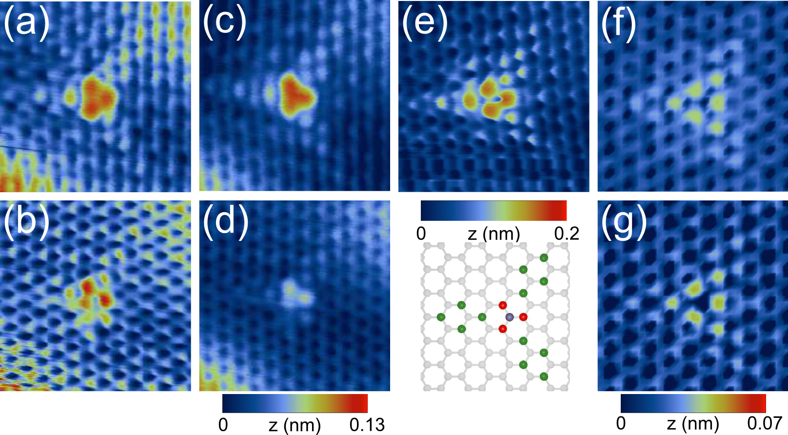
Ab initio calculations were performed to obtain the local electronic structure and the STM images using a Tersoff-Hamann approach. Calculations have been performed on a (99) supercell (0.6% of N atoms) and a (1010) supercell (0.5% of N atoms) with localized basis as implemented in the SIESTA package Sánchez-Portal et al. (1997) (see more details in the Supplemental Material and references 12-19 therein). The simulated patterns (Fig. 2(f-g); see also refs Zheng et al., 2010; Zhao et al., 2011) present a dark (low) spot above the doping atom, surrounded by bright dots, corresponding to the adjacent C atoms. The central dark spot has been explained by charge transfer from the N atom to the neighboring C atoms which results in a smaller spatial extension of the electronic states associated with the N atom in the direction perpendicular to the layer compared to the one associated with the C atoms forming the C-N bonds Zheng et al. (2010). This central ‘hole’ is not observed in most STM images (Fig. 2 and ref Zhao et al., 2011) but both the weak dependence of the pattern shape with the bias voltage and the more intense corrugation for positive biases are reproduced by simulations. Generally speaking, the limit of our computation procedure, besides the intrinsic approximations of DFT, are the simplified tip (a ‘metallic’ ‘s’ shape atomic orbital) and, more important in the present study, the small distance between the tip and the atomic layer. For numerical reasons, this distance is smaller than 3-4 Å in the simulations i.e. close to point contact and underestimated with respect to the experimental distance.
Interestingly, the hole at the center of the defect (the N atom in chemical substitution) appears in some of the experimental images, like Fig. 2(b), i.e. at low negative bias (see also Supplemental Material). By varying more extensively the experimental conditions, the same pattern has been observed for V=+0.35 V and high current (Fig. 2(e)). In all these cases (low V or high current), the tip is close to the surface and a better agreement with the simulations is expected, and is indeed observed. The tip is also closer to the surface for negative bias than for positive bias because of the localization of the energy state associated with the defect in the conduction band (see below). This explains why a plain triangular pattern is observed for V=+0.5 V whereas a hollow pattern is observed at V=-0.2 V.

Further insight regarding the local electronic structure of the dopant can be gained through STS spectra (Fig. 3 (a) with the corresponding image on fig. 3 (b)). The spectra display two minima: one at the Fermi energy (0 V), associated with phonon-mediated inelastic channels Zhao et al. (2011); Zhang et al. (2008), and one corresponding to the Dirac energy at -0.5 V. The relationship between the charge carrier concentration , the Dirac energy and the Fermi Velocity () leads to electrons per cm2 for . Assuming 0.6% of nitrogen atoms, the charge transfer can be estimated to 0.8 electron per dopant atom. From a theoretical viewpoint, our simulations for a 0.6% doping (Fig. 3 (c)) exhibit at -0.42 eV and then a smaller charge transfer (0.55 electron per N atoms). These values are larger than those reported by Zhao et al. Zhao et al. (2011) and the discrepancy can be explained by a number of potential sources of uncertainties: the accuracy in the determination of the nitrogen concentration as well as the position of the Dirac point, the presence of several types of doping sites and the uncertainty on the value of the Fermi velocity Hicks et al. (2011); Miller et al. (2009) on the experimental side or the absence of quasiparticle corrections 222Quasiparticle corrections have been demonstrated to lead to a 15% correction of the Fermi velocity of graphene Trevisanutto et al. (2008). Even if the GW calculations have not been performed here due to the large size of the supercell, the correction is expected to be small. and the regular spacing between the N sites in the supercell technique for the DFT calculations.
The comparison between the spectra at the nitrogen doping sites and far from it (Fig. 3 (a)), shows that a broad peak centered around +0.5 eV appears in the vicinity of the nitrogen atom ( spectra give a quantity proportional to the Local Density of State (LDOS)). To the best of our knowledge, this is the first experimental determination of the energy level of the localized state in N-doped graphene. The simulated Partial Density of States (PDOS) located on the N atom, on a C atom close to and far from the nitrogen (C and C atoms respectivily) are displayed on Fig. 3(c). The states related to the graphitic nitrogen are clearly obtained in the conduction bands but display a double peak structure at 0.15 eV and 0.50 eV. The nitrogen-nitrogen interactions in the periodical structure used in the calculation could lead to a splitting of the donor state that would not be present for randomly distributed defects Lambin et al. . The absence of quasiparticle corrections ††footnotemark: or the reduced tunneling current for low bias Zhang et al. (2008) may also explain why the low energy states are not observed. Besides, experimental STS spectra obtained for a tip above the center of the defect probably also probe the PDOS of the C atoms. Like the N PDOS, the C PDOS presents a double peak at 0.15 eV and 0.50 eV but with larger amplitude of the second one. Moreover a state localized at the C atoms appears around 1 eV and can be related to a second feature in the experimental STS.
Coming back to the experimental STS spectra, at negative bias, the signal is found to be lower above the nitrogen atom than above the graphene as shown in Fig. 3(a). At positive bias both STS spectra have comparable intensities. To reconcile those measurements with the higher corrugation above the dopant site (Figs 1 and 2), we have to keep in mind that spectra are measured with initial conditions corresponding to the setpoint used for the STM image. As a consequence, the tip is located at a larger distance from the atomic plane when a spectrum is measured above the dopant site, compared with a STS measurement on the graphene layer and the two spectra cannot be quantitatively compared. As it is expected that the nitrogen atom lies in the plane of the graphene sheet, as demonstrated by DFT simulations performed on single Zheng et al. (2010) and bilayer N-doped graphene Guillaume et al. (2012), the observed corrugation is a purely electronic effect. In such cases, the intensity of spectra are artificially reduced above the N atom due to the higher tip position. In order to overcome this difficulty of interpretation, we have measured some spectra while scanning with the STM feedback loop off, i.e. at a constant tip height. In these conditions, STS spectra exhibit a very different behavior (inset in Fig. 3 (a)). For negative bias, the spectrum recorded above the dopant is slightly larger than above the graphene layer, in agreement with what is observed on the images. For positive bias, the difference is even more spectacular with a LDOS measured at the doping site up to five times more intense than the one of graphene, strongly confirming that the doping states lie in the conduction band.
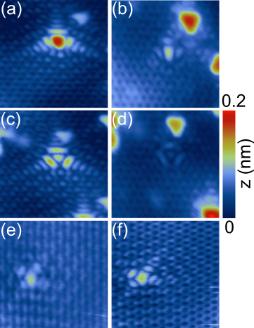
Besides the substitutional doping, other types of defects have been frequently observed, examples of which are displayed in Fig. 4. Some defects appear higher at negative bias (Fig. 4 (a) and (c)) than at positive bias (Fig. 4 (b) and (d)) contrary to what was observed for substitution. Interestingly, a simple substitutional N atom is also observed on top of Fig. 4 (a) to (d) close to the complex defects. These configurations allow a direct comparison of the bias dependence of the simple substitutional N (higher at positive bias) and of the other defects (higher at negative bias). These new dopant sites can then be associated with hole-doping and with a localized state lying in the valence band Ewels and Glerup (2005); Zheng et al. (2010). Furthermore, the experimental signature (a triangular symmetry with extended oscillations of the wavefunction) is consistent with the behavior predicted for a configuration involving three N atoms forming a pyridinic configuration Zheng et al. (2010) or with a single vacancy Amara et al. (2007). Other defects, like the one reported in Fig. 4 (e) and (f) present a pattern with a rectangular symmetry and exhibit a n-type characteristic (higher corrugation at positive bias). However, further investigations based on STS analysis are necessary to reach a definitive conclusion on the atomic configurations of these complex doping sites.
In summary, the N doping of graphene was achieved by exposing epitaxial samples to an atomic nitrogen flux. The most common (75%) doping configuration is found to be substitutional (graphitic) N atoms. Local STS Spectra have provided the first experimental evidence of a localized donor state, specific signature of N substitution. STM topographical images revealed a depletion above the N sites characteristic of a charge transfer between the N atom and the adjacent neighboring C atoms. Finally, other N doping sites with more complex atomic structure than a simple substitution were observed, exhibiting an acceptor-like character. The presented post-synthesis treatment opens the door to local tuning of electronic properties of graphene which is a prerequisite for the development of carbon-based electronics.
I Acknowledgments
F. J. thanks Jessica Campos Delgado and Benoît Hackens for the Raman measurements and Jacques Ghijsen for proofreading of the manuscript. We acknowledge fruitful discussions with Philippe Lambin, François Ducastelle and Hakim Amara. This research used resources of the Interuniversity Scientific Computing Facility located at the University of Namur, Belgium, which is supported by the F.R.S.-FNRS under convention N∘ 2.4617.07. V. R. thanks the Institut Universitaire de France for support. This work is directly connected to the Belgian Program on Interuniversity Attraction Poles (PAI6) on “Quantum Effects in Clusters and Nanowires” and to the ARC on “Graphene StressTronics” (Convention N∘ 11/16-037) sponsored by the Communauté Française de Belgique, and to the European Commission through the ETSF e-I3 project (Grant No. 211956).
References
- Castro Neto et al. (2009) A. H. Castro Neto, F. Guinea, N. M. R. Peres, K. S. Novoselov, and A. K. Geim, Rev. Mod. Phys. 81, 109 (2009).
- Liu et al. (2011) H. Liu, Y. Liu, and D. Zhu, Journal of Materials Chemistry 21, 3335 (2011).
- Fuhrer et al. (2010) M. S. Fuhrer, C. N. Lau, and A. H. MacDonald, MRS Bulletin 35, 289 (2010).
- Ewels and Glerup (2005) C. P. Ewels and M. Glerup, J. Nanosci. Nanotechnol. 5, 1345 (2005).
- Lherbier et al. (2008) A. Lherbier, X. Blase, Y.-M. Niquet, F. Triozon, and S. Roche, Phys. Rev. Lett. 101, 036808 (2008).
- Zheng et al. (2010) B. Zheng, P. Hermet, and L. Henrard, ACS Nano 7, 4165 (2010).
- Wang et al. (2010) Y. Wang, Y. Shao, D. Watson, J. Li, and Y. Lin, ACS Nano 4, 1790 (2010).
- Soin et al. (2011) N. Soin, S. S. Roy, S. Roy, K. S. Hazra, D. S. Misra, T. H. Lim, C. J. Hetherington, and J. A. McLaughlin, J. Phys. Chem. C 115, 5366 (2011).
- Reddy et al. (2010) A. L. M. Reddy, A. Srivastava, S. R. Gowda, H. Gullapalli, M. Dubey, and P. M. Ajayan, ACS nano 4, 6337 (2010).
- Cho et al. (2011) Y. J. Cho, H. S. Kim, H. Im, Y. Myung, G. B. Jung, C. Lee, J. Park, M.-H. Park, J. Cho, and H. S. Kang, The Journal of Physical Chemistry C 115, 9451 (2011).
- Kasry et al. (2010) A. Kasry, M. A. Kuroda, G. Martyna, G. Tulevski, and A. a. Bol, ACS Nano 4 (7), 3839 (2010).
- Wei et al. (2009) D. Wei, Y. Liu, Y. Wang, H. Zhang, L. Huang, and G. Yu, Nano Lett. 9, 1752 (2009).
- Zhao et al. (2011) L. Zhao, R. He, K. T. Rim, T. Schiros, K. S. Kim, H. Zhou, C. Gutiérrez, S. P. Chockalingam, C. J. Arguello, L. Pálová, et al., Science 333, 999 (2011).
- Panchakarla et al. (2009) L. S. Panchakarla, K. S. Subrahmanyam, S. K. Saha, A. Govindaraj, H. R. Krishnamurthy, U. V. Waghmare, and C. N. R. Rao, Advanced Materials 26, 4726 (2009).
- Meyer et al. (2011) J. C. Meyer, S. Kurasch, H. J. Park, V. Skakalova, D. Künzel, A. Groß, A. Chuvilin, G. Algara-Siller, S. Roth, T. Iwasaki, et al., Nat Mater 10, 209 (2011).
- Guo et al. (2010) B. Guo, Q. Liu, E. Chen, H. Zhu, L. Fang, and J. R. Gong, Nano Lett. 10, 4975 (2010).
- Lin et al. (2010) Y.-C. Lin, C.-Y. Lin, and P.-W. Chiu, Appl. phys. Lett. 96, 133110 (2010).
- Jeong et al. (2011) H. M. Jeong, J. W. Lee, W. H. Shin, Y. J. Choi, H. J. Shin, J. K. Kang, and J. W. Choi, Nano Lett. 11, 2472 (2011).
- Forbeaux et al. (1999) I. Forbeaux, J.-M. Themlin, and J.-M. Debever, Surf. Science 442, 9 (1999).
- de Heer et al. (2007) W. A. de Heer, C. Berger, X. Wua, P. N. First, E. H. Conrada, X. Li, T. Li, M. Sprinklea, J. Hassa, M. L. Sadowski, et al., Solid State Commun. 143, 92 (2007).
- Varchon et al. (2008) F. Varchon, P. Mallet, L. Magaud, and J.-Y. Veuillen, Phys. Rev. B 77, 165415 (2008).
- Hiebel et al. (2008) F. Hiebel, P. Mallet, F. Varchon, L. Magaud, and J.-Y. Veuillen, Phys. Rev. B 78, 153412 (2008).
- Starke and Riedl (2009) U. Starke and C. Riedl, J. Phys.: Condens. Matter 21, 134016 (2009).
- Sánchez-Portal et al. (1997) D. Sánchez-Portal, P. Ordejón, E. Artacho, and J. M. Soler, Int. J. Quantum Chem. 65, 453 (1997).
- Zhang et al. (2008) Y. Zhang, V. W. Brar, F. Wang, C. Girit, Y. Yayon, M. Panlasigui, A. Zettl, and M. F. Crommie, Nat Phys 4, 627 (2008).
- Hicks et al. (2011) J. Hicks, M. Sprinkle, K. Shepperd, F. Wang, A. Tejeda, A. Taleb-Ibrahimi, F. Bertran, P. Le Fèvre, W. A. de Heer, C. Berger, et al., Phys. Rev. B 83, 205403 (2011).
- Miller et al. (2009) D. L. Miller, K. D. Kubista, G. M. Rutter, M. Ruan, W. A. de Heer, P. N. First, and J. A. Stroscio, Science 324, 924 (2009).
- (28) P. Lambin, H. Amara, F. Ducastelle, and L. Henrard, in preparation.
- Guillaume et al. (2012) S.-O. Guillaume, B. Zheng, J.-C. Charlier, and L. Henrard, Phys. Rev. B 85, 035444 (2012).
- Amara et al. (2007) H. Amara, S. Latil, V. Meunier, P. Lambin, and J.-C. Charlier, Phys. Rev. B 76, 115423 (2007).
- Trevisanutto et al. (2008) P. E. Trevisanutto, C. Giorgetti, L. Reining, M. Ladisa, and V. Olevano, Phys. Rev. Lett. 101, 226405 (2008).