A hybrid superconductor-normal metal electron trap as a photon detector
Abstract
A single-electron trap built with two Superconductor (S) - Insulator (I) - Normal (N) metal tunnel junctions and coupled to a readout SINIS-type single-electron transistor A (SET A) was studied in a photon detection regime. As a source of photon irradiation, we used an operating second SINIS-type SET B positioned in the vicinity of the trap. In the experiment, the average hold time of the trap was found to be critically dependent on the voltage across SET B. Starting in a certain voltage range, a photon-assisted electron escape was observed at a rate roughly proportional to the emission rate of the photons with energies exceeding the superconducting gap of S-electrodes in the trap. The discussed mechanism of photon emission and detection is of interest for low-temperature noise spectrometry and it can be of relevance for the ampere standard based on hybrid SINIS turnstiles.
In the past few years, a significant progress has been achieved in the single-charge-manipulating circuitry based on ultrasmall tunnel junctions between superconductors (S) and normal metals (N). Currently, circuits based on a hybrid SINIS (”I” denotes the insulating tunnel barrier) single-electron turnstile Pekola2008 are considered for a variety of the current-standard applications. Reliability of single-charge manipulations has been recently dramatically enhanced due to an engineered low-temperature environment ensuring a high degree of rejection of external electromagnetic noise Camarota2012 ; Saira2012 ; Kemppinen2011 ; Lotkhov-LT26 .
A two-junction hybrid R-SINIS electron trap (”R” stands for a high-ohmic resistor in series with the junctions, see, for the details, Refs. Lotkhov2009 ; Lotkhov2011 ) probed by a SINIS-type single-electron transistor (SET) was found sensitive to the spectrum of the residual noise. On the other hand, a high degree of noise suppression made it possible to resolve the back-action of small SET currents to the hold times of the trap. Basically, the effect of SET on the neighboring circuitry arises either in the form of electromagnetic noise generated by the tunneling process (see, e.g., in Ref. Korotkov1994 for a case of non-dissipative environment) or due to the heat flow mediated by the substrate phonons (see Ref. Krupenin1999 and references therein). The related random telegraph noise (RTN) model of the SET back-action to the SINIS trap was recently proposed in Refs. Saira2012 ; Kemppinen2011 . In practical terms, the interaction mechanisms between SETs on chip are gaining in importance in view of parallelization of the SINIS turnstiles on chip for the current standard 10turnstiles . Another interesting application could involve a spectral analysis of low-temperature blackbody radiation within cryogenic setups.

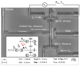
In this Letter, we suggest a mechanism of the SET backaction which is directly related to the dissipative properties of its electromagnetic environment and the photon exchange between interacting single-electron devices. In particular, we demonstrate operation of an electron trap as a detector of absorbed photons generated on chip by an adjacent SINIS SET. A two-transistor arrangement was used for this purpose with the R-SINIS trap marked as ”Detector” in Fig. 1. The trap was, on the one hand, optimally coupled to a readout SET A biased at a small probing current and, on the other hand, to an emitter SET B biased at a current as used to stimulate the photon-activated electron escape in the trap.

An electron escape from (see inset in Fig. 1) or tunneling to the trapping node involves the creation of two quasiparticles in sequence; the first one with the energy sufficiently high to overcome the electrostatic barrier formed by the SINIS double junction: , where is the superconducting energy gap in the S-leads. The background (”dark”) rate of escape strongly depends on the barrier height and on the noise level in the measuring setup. The barrier height is tunable by the source and gate voltages, from zero to the upper limit approaching the charging energy of the trap, where is a total capacitance of the small N-island in the SINIS double junction. For the measuring setup and the samples in this work (in particular, due to the relatively high resistance value of Cr microstrip 600 k), the hold times of a few hundreds of seconds were registered at the highest barrier settings. Also, impractically high values of were necessary to stimulate the escape process, unless the electrostatic barrier was tuned close to zero, , the quasiparticle states involved close to the bottom of the excitation band , and the dark hold times were reduced by two orders of magnitude down to the convenient experimental scale of a few seconds.

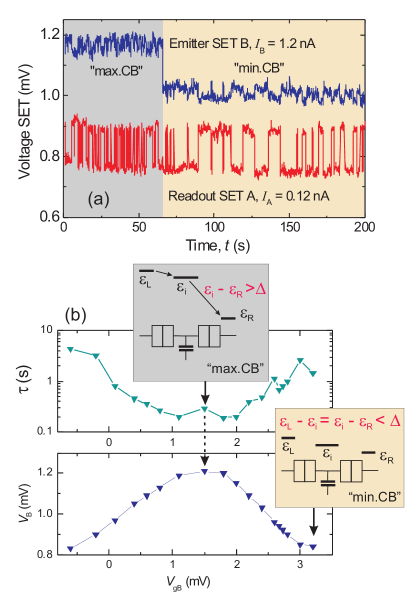
Under these conditions, we were able to observe a clear voltage dependence of the hold time , where is the voltage across SET B. This effect is demonstrated in Fig. 2(a) showing simultaneous time tracks for the voltage output of the readout SET A and the emitter SET B. A random jump to an operating point with a lower voltage 1 mV resulted in noticeably less frequent state switchings in the trap. This dependence was further verified by deliberate gate modulation of the voltage , at fixed bias current , showing correlation with the hold times , see Fig. 2(b). In this measurement, the direct electrostatic influence of the gate of SET B on the trap was compensated by a cross-cancellation signal at the source terminal. Remarkably, the maximum values of the hold times, 5 s in this plot are close to the dark values with the emitter switched off, and the minimum values are about an order of magnitude lower.
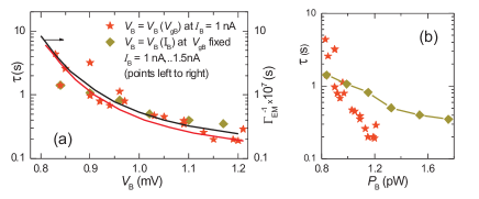
In order to draw conclusions about the direct heat transfer through the substrate (cf., e.g., Ref. Krupenin1999 ), we plotted the same hold time data as a function of either voltage , see Fig. 3(a), or the dissipated power shown in Fig. 3(b). Two data sets measured: the fixed-current data set and the incremental-current data do not collapse into a single curve along the power axis in the plot (b), but they do collapse along the -axis in the plot (a). Moreover, the slower ramping within the incremental-current data set in Fig. 3(b) would act counterintuitive, should we account for a more intensive heating due to the increasing current . A comparison with Fig. 3(a) allows us to conclude that rather the voltage , but not the dissipated power is a relevant parameter describing the influence of the emitter SET B on the trap.
We interprete the dependence following the argument of the Environment-Assisted Tunneling (EAT) approach developed in Ref. Pekola2010 . We attribute the state switchings of the trap to absorption of photons with energy 60 GHz first released during the process of electron tunneling in SET B into the biasing leads and the other circuit components constituting the electromagnetic environment (bath) of SET B IngNaz . For the purpose of modeling, we assumed an energy-independent trap switching probability per incident photon which is obviously much lower than unity.
The photon emission rate was estimated using the standard master equation treatment of SET B in a simplified form of a two-state approximation, see the symbolic pictographs in Fig. 2(b): The basic transport algorithm is considered with one tunneling event occurring in each of two junctions in sequence. The emission rate is found as a fraction of the corresponding tunneling rate , where is a free energy difference for the incoming and the consequent outgoing tunneling event to/from the SET island, respectively:
| (1) |
where
| (2) |
Here we use the standard Fermi factor in the N-island as and assume the quasiparticle band population to be negligible in the long S-leads described by BCS density of states: . The electron overheating in the 1.5 m-long N-island was accounted for, using the temperature as a sensitive fitting parameter. The device parameters are taken directly from the measurements. For the spectral function , we use its gamma-function representation developed in Ref. IngoldGrabertEberhardt for a small, semi-phenomenological frequency-independent environmental impedance .
Two solid lines in Fig. 3(a) show two possible fits, with slightly different values of and the effective temperature , which appear realistic with respect to the sample design. The calculated rates mimic the experimental dependency , whereas the absolute value of the emission rate is obviously higher than the experimental values of . This obvious effect arises due to considerable thermal losses in the leads and a very weak photon coupling to the trap, being, as a structure, much smaller than the photon wavelength 1 cm.
We also consider the RTN model of the backaction Kemppinen2011 ; Saira2012 , viewing the SET island as a two-level fluctuator (TLF) and valid even in the case . This model however fails to explain the effect of the gate voltage shown in Fig. 2, because, according to the TLF model (cf. Eqs. (12,13) in Ref. Machlup1954 ), the high-frequency tail of the RTN spectrum at , responsible for the trap excitations, should not be sensitive to the duty cycle of TLF distinguishing the different gate regimes. We note that a vanishing contribution of the RTN model might be a result of a rapid decay, for Martinis1993 , of the noise-related spectral -function of the trap.
In conclusion, our analysis of the tunneling process in SINIS SET unambiguously shows proportionality between the photon emission rate and the state switching frequency of the R-SINIS trap thus operated as a microwave photon detector. Non-zero environmental impedance of the photon-emitting SET plays an important role in the interaction process with the trap. More detailed study is necessary on the on chip propagation of the photons within a dedicated circuitry as well as on the detailed spectrometric function of the trap. Of metrological interest could be a mutual accuracy impact due to the photon exchange in an array of hybrid turnstiles operating in parallel 10turnstiles .
We acknowledge useful discussions with J. P. Pekola and A. Kemppinen and experimental support from T. Weimann and V. Rogala. The research conducted within EU project SCOPE has received funding from the European Community’s Seventh Framework Programme under Grant Agreement No. 218783.
References
- (1) J. P. Pekola, J. J. Vartiainen, M. Möttönen, O.-P. Saira, M. Meschke, and D. V. Averin, Nature Phys. 4, 120 (2008).
- (2) B. Camarota, H. Scherer, M. W. Keller, S. V. Lotkhov, G.-D. Willenberg and F. J. Ahlers, Metrologia 49, 8-14 (2012).
- (3) O.-P. Saira, A. Kemppinen, V. F. Maisi, and J. P. Pekola, Phys. Rev. B 85, 012504 (2012).
- (4) A. Kemppinen, S. V. Lotkhov, O.-P. Saira, A. B. Zorin, J. P. Pekola, and A. J. Manninen, Appl. Phys. Lett. 99, 142106 (2011).
- (5) S. V. Lotkhov and A. B. Zorin, arXiv:1106.6005 (2011).
- (6) S. V. Lotkhov, A. Kemppinen, S. Kafanov, J. P. Pekola, and A. B. Zorin, Appl. Phys. Lett. 95, 112507 (2009).
- (7) S. V. Lotkhov, O.-P. Saira, J. P. Pekola, and A. B. Zorin, New J. Phys. 13, 013040 (2011).
- (8) A. N. Korotkov, Phys. Rev. B 49, 10381 (1994).
- (9) V. A. Krupenin, S. V. Lotkhov, H. Scherer, Th. Weimann, A. B. Zorin, F.-J. Ahlers, J. Niemeyer, and H. Wolf, Phys. Rev. B 59, 10778 (1999).
- (10) V. F. Maisi, Yu. A. Pashkin, S. Kafanov, J. S. Tsai, and J. P. Pekola, New J. Phys. 11, 113057 (2009).
- (11) J. P. Pekola, V. F. Maisi, S. Kafanov, N. Chekurov, A. Kemppinen, Y. A. Pashkin, O.-P. Saira, M. Möttönen, and J. S. Tsai, Phys. Rev. Lett. 105, 026803 (2010).
- (12) G. L. Ingold and Yu. V. Nazarov, in Single Charge Tunneling, edited by H. Grabert and M. H. Devoret (Plenum, New York, 1992), Chap. 2.
- (13) G. L. Ingold, H. Grabert, and U. Ebert, Phys. Rev. B 50, 395 (1994).
- (14) S. Machlup, J. Appl. Phys. 25, 341 (1954).
- (15) J. M. Martinis and M. Nahum, Phys. Rev. B 48, 18316 (1993).