First operation and drift field performance of a large area double phase LAr Electron Multiplier Time Projection Chamber with an immersed Greinacher high-voltage multiplier
Abstract
We have operated a liquid-argon large-electron-multiplier time-projection chamber (LAr LEM-TPC) with a large active area of 76 40 cm2 and a drift length of 60 cm. This setup represents the largest chamber ever achieved with this novel detector concept. The chamber is equipped with an immersed built-in cryogenic Greinacher multi-stage high-voltage (HV) multiplier, which, when subjected to an external AC HV of 1 kVpp, statically charges up to a voltage a factor of 30 higher inside the LAr vessel, creating a uniform drift field of 0.5 kV/cm over the full drift length. This large LAr LEM-TPC was brought into successful operation in the double-phase (liquid-vapor) operation mode and tested during a period of 1 month, recording impressive three-dimensional images of very high-quality from cosmic particles traversing or interacting in the sensitive volume. The double phase readout and HV systems achieved stable operation in cryogenic conditions demonstrating their good characteristics, which particularly suit applications for next-generation giant-scale LAr-TPCs.
keywords:
Liquid argon; Pure argon; Double phase; LAr TPC; TPC; LEM; THGEM; GEM; Calorimetry; Tracking; Gaseous detector; Neutrino detector1 Introduction
The design concept of the novel Liquid Argon Large Electron Multiplier Time Projection Chamber (LAr LEM-TPC) and its promising performances have been demonstrated experimentally with a detector prototype having an active area of 10 10 cm2 [1, 2]. This new type of LAr-TPC, operating in the double-phase (liquid-vapor) mode in pure argon, is characterized by its charge amplifying stage (LEM) and its projective anode charge readout system. Situated in the vapor phase on top of the active LAr volume, these latter provide an adjustable charge gain and two independent readout views, presently each with a pitch of 3 mm111Thanks to the amplification stage which yields enough charge to be shared among several readout electrodes, smaller pitch sizes can be considered.. With time information provided by the LAr scintillation, they provide a real-time three-dimensional (3D) track imaging with information and the detector acts as a high resolution tracking-calorimeter. A very high signal-to-noise ratio can be reached in the LAr LEM-TPC thanks to the gaining stage. This significantly improves the event reconstruction quality with a lower energy deposition threshold and a better resolution per volumetric pixel (voxel) compared to a conventional single-phase LAr-TPC [2], such as e.g. ICARUS [3], ArgoNeut [4] or J-PARC T32 [5]. In addition the charge amplification compensates for potential loss of signal-to-noise due to the charge diffusion and attachment to electronegative impurities diluted in LAr, which both become more important as the drift length increases. It is therefore considered to be a promising technology for the next-generation giant-scale underground detectors for neutrino physics and proton decay searches (GLACIER) [6, 7, 8] and for direct Dark Matter searches with imaging [9].
In this paper, we report on the first operation of a LAr LEM-TPC prototype having an active area of 76 40 cm2 and a drift length of 60 cm, which is the largest chamber ever realized with this novel detector concept. The detector was tested successfully in the double-phase operation mode in pure argon, recording events of cosmic tracks traversing or interacting in the active volume. The analysis of its tracking performance which requires full 3D reconstruction of a large number of recorded tracks is reported elsewhere [10], and the focus of this paper is put on the immersed high-voltage (HV) system for the drift field and cold operation.
The HV system is based on the technique of a cryogenic Greinacher [11] (also known as Cockcroft-Walton [12]) HV multiplier immersed in LAr directly inside the detector vessel. It is an innovative technique to generate a HV for creating a drift electric field in a LAr-TPC, with some advantages compared to other methods used up to now whereby the very HV is externally generated and brought into the detector via a HV feedthrough (for a comparison see Ref. [13]). This technique particularly suits a large- to giant-scale detectors, where a very HV of 100 kV to 1 MV would be needed for a drift field of 1 kV/cm over a length of 1 m to 10 m.
The main advantages of the Greinacher HV multiplier are: (1) all the HV parts are immersed in LAr which has a large dielectric strength (1 MV/cm), (2) thus feedthroughs for very HV are not needed, (3) the circuit itself can provide all the stages needed to create a uniform field, thus the system has no resistive load, (4) thus the power dissipation is virtually zero and (5) this allows a low frequency (e.g. 50 Hz) of the AC input signal which is fully outside of the bandwidth of the charge amplifiers used for this type of detectors. One main disadvantage is the difficultly of access in case of a failure. The potential impact of this access on the pure liquid argon volume can be large if the active components are directly immersed in it222It is still possible to imagine that the Greinacher circuit is located in a separately evacuable volume in contact with the main pure liquid argon volume during normal operation, but which would be disconnected and separately emptied during maintenance, with minimal impact on the main liquid argon volume, thereby still avoiding the need for a HV feedthrough..
To study in detail the functionality of such a system under practical conditions incorporated in a LAr-TPC, we built a 30-stage Greinacher HV multiplier integrated to the large-area LAr LEM-TPC prototype. We carried out the test experiment at CERN from October to December 2011 using cryogenic LAr apparatus of the ArDM Project (CERN RE18) [14], which is an experiment for a direct Dark Matter search exploiting a 1-ton-scale double-phase argon TPC [9].
In Section 2 we describe the experimental setup, i.e. the LAr LEM-TPC, the cryogenic apparatus and the HV system. Results of a series of measurements performed in air at room temperature and in LAr for characterizing the Greinacher HV multiplier are presented in Section 3. In Section 4 we report on the test experiment, where the entire LAr LEM-TPC with the HV system was tested successfully in the double-phase operation mode in pure argon. Finally we discuss and conclude on the results in Section 5.
2 Experimental setup
2.1 Design of the large-area LAr LEM-TPC
2.1.1 LAr LEM-TPC design overview
Figure 1 illustrates the structure of the LAr LEM-TPC hanging inside the ArDM detector vessel. The field cage, which defines the active LAr target and drift volume, is constructed with four PCB side walls in a shape of rectangular box with dimensions 76 cm (L) 40 cm (W) 60 cm (H). On the inner surface of each PCB 31 horizontal field shaping strips, which hereafter are called field shapers (FS), are formed by etching at a constant pitch of 20 mm. The top (FS0) and the bottom (FS30) field shapers have a width of 9 mm while the ones in between have 18 mm, with a gap of 2 mm between neighboring ones. Negative high voltages linearly decreasing from bottom to top are distributed to the field shapers so that a vertical drift electric field is created uniformly over the full drift length of 60 cm.
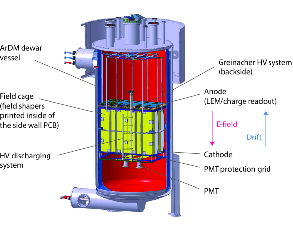
On top of the field cage two horizontal extraction grids are mounted with a gap of 10 mm in between. The grid is a 0.15-mm-thick stainless-steel mesh, where square holes with a size 2.85 2.85 mm2 are etched at a pitch of 3 mm all over the active area. The lower grid is positioned at the top face of the field cage. For the double-phase operation mode the LAr surface is adjusted at the middle of the two grids. The liquid level at each of the four corners can be monitored with a precision of 0.5 mm with the aid of four capacitive level meters. Ionization electrons produced by ionizing particles are drifted upwards to the liquid surface. These electrons are extracted across the liquid-vapor interface into the gas argon (GAr) phase with the aid of a strong extraction field of typically 3–4 kV/cm between the two grids. They are then collected by the charge readout system incorporating the Large Electron Multiplier (LEM), which is described in Section 2.1.2. The bottom face of the field cage is covered by the cathode grid that is a stainless-steel mesh of the same type as used for the extraction grids. The top (FS0) and the bottom (FS30) field shapers are electrically coupled to the lower extraction grid and respectively, to the cathode.
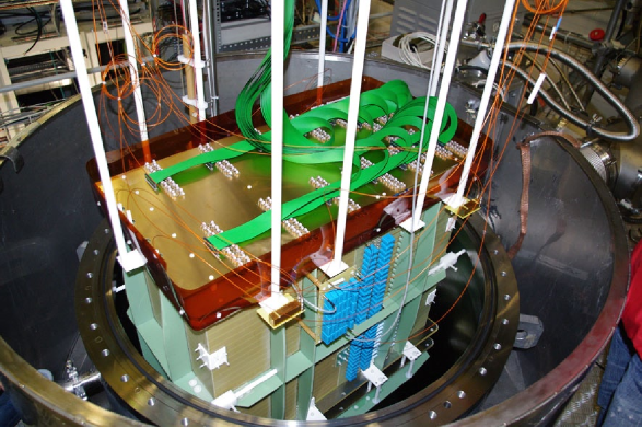
The HV for creating the drift field is generated using a built-in 30-stage Greinacher HV multiplier, which is described in detail in Section 2.3. The circuit is integrated in the design of one of the side-wall PCBs and the components are mounted directly on the outer surface of the PCB, as can be seen in Figure 2. As already mentioned the generator itself avoids the use of a voltage divider, since each multiplying stage provides a characteristic DC voltage. The various multiplying stages generate a monotonously increasing potential to supply the electrodes surrounding the drift volume. In our setup, the DC output of each of the 30 Greinacher stages is connected to each field shaper via a wire through the PCB.
Under the field cage two photomultiplier tubes (PMTs) are installed to detect scintillation light produced by charged particles crossing the LAr target (primary scintillation, S1), as well as the secondary scintillation light (S2) produced via electro-luminescence by the electrons extracted to the GAr phase [15]. We employed Hamamatsu R11065 cryogenic 3” PMTs having a high quantum efficiency of 30%, specifically designed for the use in LAr [16]. The quartz window of the PMT was coated with a wavelength shifter, 1,1,4,4-Tetraphenyl-1,3-butadiene (TPB) [17], in a Paraloid™ B-72 polymer matrix to detect deep ultra violet photons of the argon scintillation (peaked around 128 nm) . The PMT signal is used primarily for triggering and for determination of the event absolute time. To protect PMTs from possible discharges from the parts at HV, another mesh electrode, which is grounded to the detector vessel, is inserted between the cathode grid and the PMTs. The distance between the cathode and the protection grid was 9 cm and that between the protection grid and the PMTs was 1 cm.
2.1.2 LEM charge readout system
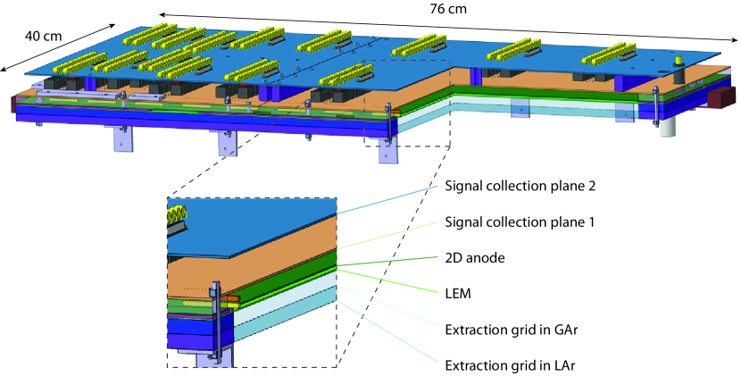
The charge readout system of the LAr LEM-TPC is a direct extrapolation of the successful 10 10 cm2 prototype [1] to an active area as large as 76 40 cm2. It is characterized by (1) a single 1-mm-thick LEM amplification stage and (2) a 2D readout anode realized on a single PCB. The system has a multi-stage structure consisting of two extraction grids, a LEM, a 2D readout anode and two signal collection planes as illustrated in Figure 3. The distances between the stages and typical configurations for the potentials and the inter-stage electric fields are summarized in Table 1. In typical configurations a positive HV of 1 kV is applied to the anode while the extraction grid in liquid is operated at a negative HV of kV, resulting in a virtual ground within the LEM plane.
| Distance to the | Typical operating | Field to the stage | |
|---|---|---|---|
| stage above (cm) | potential (kV) | above (kV/cm) | |
| Signal collection plane 2 | – | 0 | – |
| Signal collection plane 1 | 2 | 1 | – |
| 2D anode | 1 | 1 | – |
| LEM (top electrode) | 0.2 | 0.5 | 2.5 |
| LEM (bottom electrode) | 0.1 | 3 | 35 |
| Extraction grid in GAr | 1 | 4 | 1 |
| Extraction grid in LAr | 1 | 7 | 3 |
| Cathode | 60 | 31 | 0.4 |
The LEM is a macroscopic hole electron multiplier built with standard PCB techniques333It was manufactured at ELTOS Circuiti Stampati Professionali, Italy (http://www.eltos.com/).. It is a 1-mm-thick FR4 plate, double-side cladded with a passivated copper layer. Of the order of half a million holes 500 m in diameter are CNC (Computer Numerical Control) drilled through the plate at a pitch of 800 m between the centers of adjacent holes. After the PCB has been manufactured and drilled, the copper layers are further chemically etched to create 40 m wide rims around the holes. A HV of typically 3.5 kV is applied across the two faces creating a strong electric field of 35 kV/cm in the LEM holes leading to multiplication of electrons by avalanches.
The 2D anode plane has two orthogonal sets of readout strips on the bottom face providing two independent readout views. On top of the strips for one view, those for the other view are laid with a thin (50 m) polyimide (Kapton) insulating bed underneath. For each view, copper strips are formed by etching at a pitch of 600 m covering nearly the full area of 76 40 cm2. The readout pitch of 3 mm is obtained by bridging five strips at one end. The strips on top are narrower (120 m) than those lying underneath (500 m) optimizing for an equal charge collection by the two views operating at the same potential. A more detailed description of the 2D anode can be found in [1]. The strips for both of the views are tilted by 45∘ with respect to the sides of the rectangular plate, to have symmetric conditions for both views.
We use two signal collection planes, between which HV decoupling capacitors (270 pF) are connected. Each readout channel is routed to a collective 32-channel connector to a flat cable. A surge arrester protecting the readout electronics from discharges is mounted for each channel. The cables bring the signals through a custom-made feedthrough on the upper flange, connected to the readout electronics [10] placed outside of the vessel.
The LEM charge readout system is assembled as a multi-layered “sandwich” unit with precisely defined inter-stage distances and inter-alignment. The entire unit can then be mounted to or dismounted from a field cage, which may have different configurations, e.g. drift lengths.
2.2 ArDM cryogenic system
The double-phase operation of the LAr LEM-TPC requires a sophisticated cryogenic LAr apparatus which fulfills demanding conditions: (1) the LAr target must be maintained at a very high purity which corresponds to an oxygen-equivalent impurity concentration less than 1 ppb, (2) the pure argon volume must be pumped down to a high vacuum ( mbar) before filling with LAr to reduce contamination of the argon due to outgassing, (3) filling through a purification filter is obligatory, (4) to maintain and improve the purity during the test period (i.e. months), LAr must continuously be cleaned with the aid of a recirculation/purification system, (5) thermodynamical conditions, i.e. temperatures and pressures must continuously be controlled and (6) the system must be protected from possible hazards due to a large amount of cryogenic LAr in case of unexpected incidents. Therefore, we carried out the test experiment fully exploiting the cryogenic apparatus of the ArDM Experiment, which we had previously built and operated at CERN [14].
Figure 4 presents a rendered CAD picture of the apparatus. The ArDM cryogenic system consists mainly of the detector vessel and the LAr recirculation/purification system. The two sections are connected with horizontal pipings at the top and the bottom.
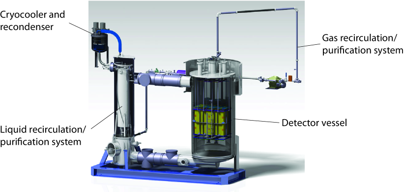
The detector vessel has an inner diameter of 1 m and a height of 2 m containing approximately 2 tons of LAr when it is full. In this test experiment the vessel was filled up to approximately two thirds of the full volume. The pure LAr volume, which is constructed as a ultra-high vacuum tight closed volume, is surrounded by a separate LAr volume serving as a cooling bath. The temperature of LAr and consequently the pressure in the cooling bath are maintained with the aid of the cryocoolers installed in the recondenser sitting on top of the recirculation/purification section. The cooling bath then is surrounded entirely by an insulation vacuum. The pure LAr is recirculated through a custom-made purification cartridge filled with activated copper powder with the aid of a cryogenic bellows LAr pump installed below the cartridge, and is purified continuously, i.e. the residual oxygen contamination is removed through a reaction . For initial filling of the vessel with LAr another custom-made cartridge of a similar type with a molecular sieve and an active copper powder layer was used. In addition a gas recirculation system incorporating a commercial SAES getter444SAES Getters S.p.A.. http://www.saesgetters.com/ is implemented in the system.
The thermodynamical conditions, i.e. pressure and temperature, at different parts of the system are monitored and logged continuously by a PLC (Programable Logic Controller) system. Furthermore the PLC system allows manipulation of various active components such as vacuum pumps, electro valves, the bellows pump and heaters to regulate the cooling power of the cryocoolers. Although the cryogenic system has a number of rupture disks as an ultimate safety measure the PLC system provides early alarms and a range of interlocks to stabilize the conditions before reaching the rupture pressure. In addition, the system can be accessed via internet allowing a remote control.
During the test experiment, the LAr temperature was maintained at 86.3 K. We reached a pressure stability better than mbar. With the electron drift velocity of 1.4 mm/s at 86.3 K and the drift electric field of 0.4 kV/cm it takes 430 s for electrons to travel over the full drift length of 600 mm of the tested LAr LEM-TPC. We ran the bellows pump for two weeks at full speed and the oxygen-equivalent impurity concentration reduced from 1.5 to 0.5 ppb. The lifetime of drifting electrons () can approximately be calculated as a function of the oxygen-equivalent impurity concentration () [18] : . The impurity concentration of 0.5 ppb leads to s.
2.3 HV system
2.3.1 Cryogenic Greinacher HV multiplier
The 30-stage cryogenic Greinacher HV multiplier was designed fully exploiting experiences gained in R&D of the ArDM HV system [13], which is based on the same concept and has 210 stages. For the main circuit components, namely capacitors and diodes, ones of the same types as in ArDM were chosen because of their known reliability in LAr. Figure 5 illustrates the diagram of the circuit. Each capacitor symbol corresponds to one single polypropylene capacitor having 82 nF and each diode symbol to a chain of three avalanche diodes connected in series. The direction of the diodes determines the polarity of the DC output voltage which is negative in this case. A single stage is designed to hold as high as 2 kVDC, i.e. the circuit is able to output a total of 60 kVDC.

The output voltage is proportional to the amplitude of sinusoidal input voltage. Fully charged the voltage across each stage reaches ideally the peak-to-peak value of the input voltage () and hence the potential at the th stage equals to . The DC output of the th stage which is denoted as in the diagram is connected to the field shaper FS (). The potential of the whole circuit can be shifted by adding a DC voltage source and several appropriate components, as shown in red in Figure 5. This is used to adjust the potential of FS0 and of the extraction grid in LAr with respect to that of the charge readout system.
The Greinacher circuit is integrated directly on the outer surface of one of the side-wall PCBs as can be seen in Figure 2. The shifting part is built on a separate PCB and is mounted near the Greinacher circuit. For the last 12 stages a HV resistor having 200 M is inserted between the Greinacher stage and the field shaper to limit the current flowing out of the large capacitances in case of an unwanted discharge from the cathode or the field shapers at very HVs. For the double-phase operation mode the whole circuit is immersed in LAr.
Table 2 summarizes the parameters of the Greinacher circuit as described above. The specifications of its components can be found in Table 3.
| Number of Greinacher stages , | 30 | – |
| Capacitance per capacitor, | 82 | nF |
| Number of capacitors | 60 | – |
| Combined capacitance | 5.5 | nF |
| Maximum rated voltage per stage | 2000 | V |
| Maximum output voltage () | 60 | kV |
| Stored charge at | 10 | mC |
| Stored energy at | 10 | J |
| Capacitor | ||
|---|---|---|
| Double metallized film pulse capacitor, polypropylene dielectric | ||
| Manufacturer | Evox Rifa555Evox Rifa GmbH. http://www.evoxrifa.fi/ | |
| Type | PHE450 | |
| Winding construction | Two Section | |
| Lead spacing | 22.5 | mm |
| Dimensions | 11.0 21.5 26.0 | mm3 |
| Rated voltage DC | 2000 | VDC |
| Capacitance | 82 | nF |
| Diode | ||
| High-voltage soft-recovery rectifier (avalanche diode) | ||
| Manufacturer | Philips Semiconductors666NXP Semiconductors. http://www.nxp.com/ | |
| Type | BY505 | |
| Package | Rugged glass package | |
| Maximum ratings | ||
| Peak reverse voltage (65 … 120 ∘C) | 2200 | V |
| Non-repetitive peak forward current | 5 | A |
| Repetitive peak forward current | 800 | mA |
| Average forward current777Averaged over any 20 ms period at 25 ∘C. | 85 | mA |
| Electrical characteristics | ||
| Diode capacitance (0 V) | 2 | pF |
2.3.2 AC power supply unit
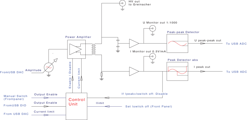
A dedicated power supply unit was developed to supply appropriate AC voltages for charging Greinacher circuits for LAr-TPCs. Its block diagram is shown in Figure 6 and the relevant specifications are summarized in Table 4.
The AC power supply unit is controlled and monitored through a USB interface by a commercial PC. The amplitude of the sinusoidal output voltage can be ramped up from 0 to 2.7 kVpp (peak-to-peak) with a maximum current of 10 mA (r.m.s.). A fixed frequency of 50 Hz for the output signal is generated by a quartz oscillator. The ramp-up rate of the output voltage can be set in the range from 10 to 1000 V/s. The output voltage and current are measured by a peak-to-peak detector and an absolute peak detector, respectively, and are read out via USB. On the front panel there is an analog output for each of the output voltage and current to allow monitoring of their waveforms on an external oscilloscope.
The internal control unit can be enabled/disabled either by the USB interface or by a manual push-button switch on the front panel. The peak output current is set by the interface through the control unit. If a sudden discharge of the Greinacher capacitors generates an over-current in the secondary coil of the transformer, the control unit turns off the system. This current limit is set by a potentiometer on the front panel. The power amplifier is also protected for over-voltages. The system has never been damaged even though a few discharges occurred while testing several different Greinacher circuits.
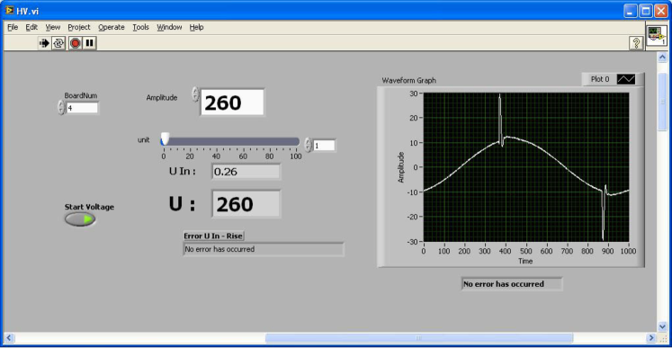
A software to control the AC power supply unit was built based on LabView888LabView, National Instruments Corporation. http://www.ni.com/labview/. It has a graphical interface as shown in Figure 7, where one can type in the set value for the peak-to-peak output voltage and can start/stop charging by pressing a button. The ramp-up rate of the output voltage can also be set using the interface. The monitored value of the peak-to-peak voltage and a waveform of the output current for one cycle of the sinusoid are displayed on the window.
| Output | ||
| Frequency | 50 | Hz |
| Voltage | 0 … 2700 | Vpp |
| Maximum peak current (r.m.s.) | 10 | mA |
| Transformer | ||
| Manufacturer | Josef Betschart AG999Josef Betschart AG. http://www.betschart-trafo.ch/ | |
| Type | TET 84a/10852 | |
| Power rating | 20 | VA |
| Primary circuit (input) | ||
| Maximum voltage (r.m.s.) | 30 | V |
| Maximum current (r.m.s.) | 780 | mA |
| Secondary circuit (output) | ||
| Maximum voltage (r.m.s.) | 2 | kV |
| Maximum current (r.m.s.) | 10 | mA |
| Monitoring output | ||
| Voltage monitor | 1 | V/kV |
| Current monitor | 0.5 | V/mA |
2.3.3 Discharging system
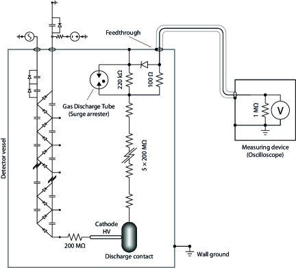
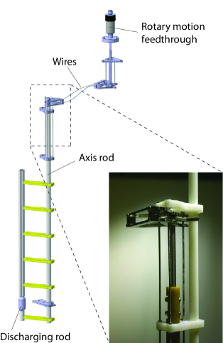
A similar system as reported in [13] was built to actively and safely discharge the Greinacher circuit. Its circuit diagram and the mechanics are presented in Figure 8. A mechanical switch realized with a rotating discharging rod steered by a rotary motion feedthrough makes contact between the cathode and a resistor chain of total of 1 G which is connected to the top flange of the dewar at the other end. The resistance is chosen to discharge the circuit completely in the order of 10 s and to keep the peak discharging current small enough compared to the maximum rating for the forward current through the diode. The cathode voltage and the discharging current decreases with an exponential decay at a decay constant s which is determined by the chain resistance G including the resistor inserted between the Greinacher circuit and the cathode and the combined capacitance nF of the Greinacher circuit. The peak current for discharging from 60 kV is 50 A.
The newly developed mechanics have a cable-pull system like a bicycle brake, i.e. the axis rod and the feedthrough shaft are connected with two stainless steel wires through two fixed stainless steel tubes. Thanks to this new technique the wires can be routed flexibly providing a large freedom in choosing the location of the discharging rod independent of the position of the feedthrough.
Such a discharging system allows not only discharging the circuit but even more importantly a direct measurement of the cathode voltage by measuring the peak value of the discharging current. The discharging current can be measured by recording the voltage across the 220 k reading resistor inserted between the discharging resistor chain and the ground. The measured peak voltage is equal to 0.15 per mil of the cathode voltage, e.g. 1.5 V is measured for 10 kV. A surge arrester and a Zener diode are connected in parallel to the reading resistor to protect the measuring device, which is usually an oscilloscope.
3 Characterization of the Greinacher HV multiplier
3.1 Theoretical model
The total output voltage expected from a Greinacher chain is ideally equal to the value of the input peak-to-peak AC voltage multiplied by the number of stages. Under real conditions however, the output voltage can be smaller. Losses are mainly due to effective capacitances of the diodes and several stray capacitances which depend on the actual geometrical setup. Altogether the “shunt” capacitance is the capacitance between the AC side (the top row in the diagram in Figure 5) and the DC side (the bottom row) of the Greinacher circuit. In a transmission line model, which can be found in [19, 20] and also in [13] the joint effects of charge dissipation in an external load resistance and charge in the shunt capacitances can be calculated to yield the total output voltage, given as
| (1) |
is the number of stages, the frequency of the input voltage generator, the resistive load (assumed to be equally distributed on each stage), the shunt capacitance (parallel to each diode) and the capacitance of a single capacitor element. The slope of the Greinacher output equals to . Neglecting the resistive load contribution, the shunt capacitance can be estimated directly from it.
In the actual ArDM setup, where the Greinacher is connected to the field shaping rings and the cathode, we can expect surface leakage currents which can affect the response of the Greinacher circuit, acting as a load. We first performed a set of measurements in air and in liquid argon with the circuit disconnected from the ArDM setup, as described in the next Section.
3.2 Charging up of the circuit at room and LAr temperatures
Before assembling the whole TPC we tested the Greinacher circuit alone – not connected to the field cage – in air at room temperature and in a polystyrene container open to the atmosphere and filled with LAr for characterizing the circuit. For measuring the output HV we used a custom-made field mill [21, 22], which is a capacitive device allowing measuring the output voltages of the Greinacher circuit without drawing any current. Such a feature is very important since a resistive load resulting in a small current connected to the Greinacher circuit changes its behavior.
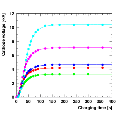
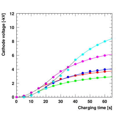
Figure 9 shows thus measured output voltage at the cathode (i.e. the Greinacher stage No. 30) while the circuit was charging up. Different curves are for different input AC voltages, i.e. 150 Vpp (red) and 250 Vpp (magenta) in air and 150 Vpp (green), 200 Vpp (blue) and 400 Vpp (cyan) in LAr. The horizontal axis shows the time after the AC voltage source was turned on. The input AC voltage was ramped up at a fixed rate of 10 V/s throughout the operation of the system. The trend of the increase of the voltage at the first part of each curve thus is determined by the ramp-up rate and is independent of the input voltage, as can be seen clearly in the zoom for the first 65 s shown in the right plot in Figure 9. This trend however is different between in air and in LAr due to the threshold effect of the diodes in cold (see also Section 3.3). For each of the two temperatures it was parametrized with a polynomial function and is shown with a dotted curve.
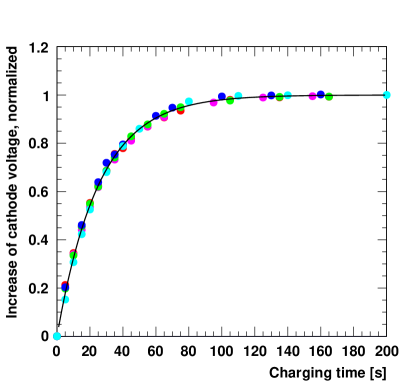
To see a general trend of charging of the circuit discarding the effect of the ramp-up rate of the AC power supply, the increase of the output voltage after the set value of the input voltage was reached is plotted in Figure 10. The increase of the voltage is normalized to the difference between the voltage measured when the set value was reached and the finally reached voltage. Thus all the curves shown in Figure 10 lie on a single curve and fit very well with an exponential function, implying that the charge-up time was approximately independent of the input/output voltages and also of the temperature. Fitting all the points with an exponential function the time constant for the charge up of the circuit was found to be 26 s, i.e. the circuit was charged up to 99% of the final value in 120 s after the input AC voltage reached the set value.
3.3 Linearity of the DC output voltage as a function of the AC input voltage
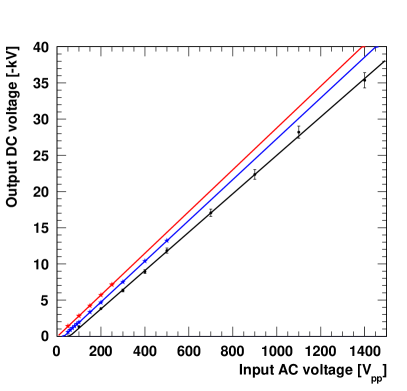
Figure 11 shows the output DC voltage measured at the last stage of amplification as a function of the peak-to-peak input AC voltage in air at room temperature (red) and in LAr (blue). The points measured in air agreed well with a linear dependence between the output and input voltages over the whole range of the tested output voltages up to 7.5 kV. The curve for LAr was shifted towards higher input voltage by 33 Vpp showing the threshold effect of the diodes in cold, i.e. the diode drew forward current only when the voltage across the three series diodes exceeded the threshold value. However a linear dependence was verified also in LAr up to 13.5 kV output although at lower voltages the points showed a small deviation, and therefore the points below 100 Vpp were excluded from the fit. The slopes obtained from a linear fit were 28.9 V/V in air and 28.2 V/V in LAr, respectively. In the ideal case the slope equals to the number of the Greinacher stages, i.e. 30. The shunt capacitances obtained from the slopes (Eq. 1) were 2.7 and 4.4 pF for in air and in LAr, respectively. For an identical geometrical configuration, a larger value in LAr is expected because of its relative dielectric constant of 1.5. The remaining difference is due to a dissimilar capacitance between the Greinacher circuit and the surrounding ground in the two setups (air and LAr configuration).
3.4 Linearity of the voltage distribution across the multiplying stages
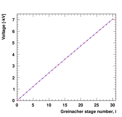
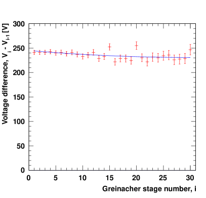
The linearity of the voltage distribution over the field shapers is the first indicator of the uniformity of the drift field. Potentials at different Greinacher stages charged at 250 Vpp were measured in air at room temperature. A linear behavior of the Greinacher stage voltages was obtained, as shown in the left plot in Figure 12. On the right plot, red points show the measured voltage differences between neighboring Greinacher stages. The error shown in the plot corresponds to 0.1% of each measured voltage of field shapers. The blue curve is calculated using a transmission line model with a shunt capacitance of 2.7 pF as described in the previous section. The expected reduction of the voltage across the last Greinacher stage with respect to that of the first stage is 6%. The measured values were in good agreement with expectation although a few points deviated by 10%. The expected reduction can be as large as 10% in LAr from the calculation based on the shunt capacitance of 4.4 pF (Section 3.3).
3.5 Characterization of the HV system with the discharging method
The cathode voltage, measured by discharging the Greinacher circuit using the discharging system, as described in Section 2.3.3, can be used effectively to characterize the HV system. A series of dedicated measurements were performed with the fully assembled setup in ArDM.
A typical example of a measured curve is shown in Figure 13. The sharp peak at s shows the fast discharging of the cathode grid. It is followed by a slower exponential decrease of the voltage due to discharging of the Greinacher circuit through the current limiting resistor (200 M) in addition to the discharging resistor chain (1 G), as described in Section 2.3.3. The discharging curve measured across the reading resistor was fitted with an exponential function for s. The intercept is proportional to the cathode voltage before discharging. The shown curve was obtained for the circuit charged at 1400 Vpp input AC voltage and V corresponds to the cathode voltage of kV. The measured decay constant s is consistent with the naive calculation of s (see Section 2.3.3), taking into account possible temperature variations of the capacitors and additional stray-capacitance of the ArDM setup.
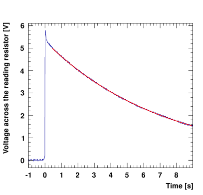
To measure the output voltage as a function of peak-to-peak input AC voltage the Greinacher circuit was charged up at different input voltages and then discharged recording the discharging curve. The measured points are plotted in black in Figure 11. Voltage measurements using the discharging current clearly had a larger error compared to those using the field mill. The errors were dominated by those on the resistances and on the determination of the intercept by the fit and were found to be 3% of the measured voltages. Within the measurement precision a linearity of the output voltage to the input voltage was verified up to the input AC voltage of 1400 Vpp which resulted in the output voltage of kV (from the linear fit for the input voltages 200 Vpp) and the drift electric field of 0.6 kV/cm. The slope of the linear fit was found to be 26.5 V/V, somewhat smaller than that obtained from the measurements with the Greinacher circuit alone in LAr (blue). The observed reduction of the slope by cannot be attributed to a resistive load, which is constrained by the observed discharging time (see Section 4.1) to be . It can be described by two effects: (1) the presence of the DC-voltage shifting circuit which decreases the slope by 3%; (2) a capacitive contribution of the dewar inner surface and the field shapers to the shunt capacitance. It should be noted that the measured output voltages will be confirmed by the drift velocity measurements, as shown in Section 4.
We also investigated the charging curves at the input AC voltage of 500 Vpp and 900 Vpp. Each point was measured in such a way that the input AC power supply was turned off at a certain time, while the Greinacher circuit was still charging, and then the circuit was discharged and the cathode voltage was measured from the discharging current. The behavior was found to be similar to that shown in Figure 9, with the first part determined by the ramp-up rate of the input AC voltage followed by the second part consistent with an exponential function. The time constant of the exponential part was also consistent with that obtained from Figure 10 and showed that the circuit was fully charged 2 minutes after the set value was reached at the input AC power supply.
3.6 Characterization of the HV DC-shifting circuit
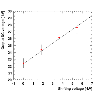
To check the functionality of the DC-voltage shifting circuit the cathode voltage was measured with the discharging method, while the shifting DC HV was applied at different offset values as plotted in Figure 14. The measurements agreed with the expected values (dotted curve) verifying a linear increase of the cathode voltage depending on the offset voltage within the measurement precisions.
4 Operation of the LAr LEM-TPC in the double-phase mode
4.1 Drift velocity based on scintillation light measurements
The LAr LEM-TPC was operated in the double-phase mode in pure argon for a continuous period of about a month, recording cosmic track events (a large fraction were vertically traversing muons) with the PMTs and the LEM charge readout system. The drift electric field was created using the built-in Greinacher HV system and was maintained essentially throughout the experiment. The Greinacher circuit was re-charged periodically. The recording of cosmic events could be done when the charging AC power supply was on or off. The natural decay rate of the HV in the system was measured several times during the experiment and was found to be consistent with an exponential decay with a time constant of the order of 5–10 days. Since the natural decay rate is very slow, changes of the drift field were negligible for a few hours of measurements even when the AC power was off.
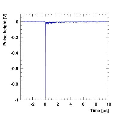
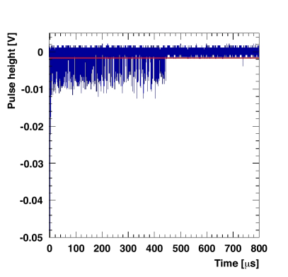
With the drift of electrons and their extraction across the liquid-vapor interface, signals of ionization in LAr can be detected using the PMTs through the S2 secondary scintillation light. It should be noted that the LAr LEM-TPC prototype was not fully optimized for light readout. The solid angle coverage by the photocathode of the PMT for the S2 light was only 0.05%, the extraction region being located at the distance of 70 cm from the PMT, but was sufficient to detect clear primary (S1) and secondary (S2) signals, and in particular, their time distribution. Typical recorded waveforms for the S1 and S2 are shown in Figure 15. The two histograms correspond to the same cosmic event taken with a drift field of 355 V/cm. The S1 signal is used to determine the event time ( s). The S2 signal consists of single photoelectron pulses distributed over several hundred microseconds, corresponding to the different drift times of the recorded hits. The red line in the right figure shows a typical threshold value (corresponding to 0.25 p.e.) used to discriminate PMT pulses from the noise.
Figure 16 shows the time distribution of PMT pulses for cosmic events triggered with the PMT itself, obtained for four different values of the drift field, i.e. 443 V/cm (magenta), 355 V/cm (blue), 266 V/cm (green) and 178 V/cm (red). The vertical axis shows the number of PMT pulses above the threshold 0.25 p.e. regardless of their pulse heights. The pulse counts are normalized to the highest peak at s (), which corresponds to the primary scintillation light (S1). In this way the visibility of the S2 signals can be enhanced despite the fact that they mostly consist of a bunch of single photoelectron pulses distributed over several hundreds of microseconds. It is worth mentioning that, to ensure a pulse linearity for a large signal, relatively large capacitances were connected to the four last dynode stages. A polypropylene capacitor having 22 nF was used for the dynode 9 and 10, and 122 nF for the dynode 11 and 12. No evidence of a gain reduction was seen after a very strong S1 pulse (see Figure 15) with these capacitors.
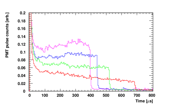
The S1 peak is followed by the S2 signal continuing until the maximum drift time which depends on the drift field, and can be seen as clear edges in Figure 16. This maximum drift time corresponds to the time when the ionization electrons generated in the vicinity of the cathode grid, i.e. the bottom of the field cage, arrive at the LAr surface and are extracted into GAr. While only those muons which cross both, the top and bottom face of the field cage create S2 signals over the full drift time ( to ), “grazing” muons which cross one or two of the side walls produce an S2 distribution having a smaller width. However, the edge is clearly visible when enough events are accumulated, because of the fact that there can be no extraction after . Since the drift velocity is a function of electric field () and of LAr temperature (), also depends on those two parameters
| (2) |
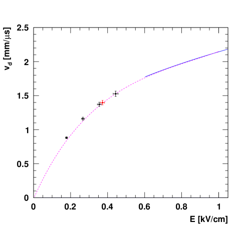
where is the height of the field cage, i.e. mm. The electron drift velocities thus calculated from the measured are plotted with black dots in Figure 17 as a function of drift electric field. The drift field was calculated based on the peak-to-peak value of the input AC voltage using the linear function obtained from the output voltage measured as a function of the input voltage, which is described in Section 3.5. The horizontal error bars correspond to of the calculated cathode voltage and the vertical ones s in the measurement of . We compare our measurements with the ones obtained with ICARUS purity monitors at low electric fields [23] taken at 89 K. In order to estimate the drift velocity at the temperature of 86.3 K of our setup obtained from the measurements using the PLC system (see Section 2.2), we employed the correction [24] to scale the fifth order polynomial, obtained from a fit to the low field measurements [23]. Our points agree well with the polynomial function, as shown in Figure 17.
4.2 Drift velocity and uniformity based on ionizing tracks measurements
The LEM charge readout system operated successfully in double-phase mode. Three examples of cosmic events obtained with typical electric field configurations (the drift field of 0.4 kV/cm and 35 kV/cm in the LEM holes, see Table 1) are presented in Figure 18. Using a simple event display images for two projections, i.e. - and -projections, can be obtained for each event: - and -coordinates are two horizontal coordinates orthogonal to each other and -coordinate corresponds to the vertical coordinate . From a visual inspection, the effective gain of the readout is above 15 for best field configurations, consistent with results obtained on the smaller detector prototype having an active area of 10 10 cm2 [1, 2]. A quantitative analysis will be reported elsewhere [10]. The maximum drift time can be directly determined from those tracks, i.e. the edge is clearly visible in a time distribution of the charge signals. The corresponding drift velocity is shown in Figure 17 (with a red dot) and is in a good agreement with the other measured points.


To evaluate the uniformity of the drift electric field along the vertical coordinate, cosmic muon tracks recorded using the LEM charge readout system were analyzed. Figure 19 shows a time distribution of the hits for 147 fully reconstructed tracks. The number of readout channels giving a charge signal above threshold (i.e. a hit) within each time bin was counted and put into the histogram. The data were taken with the typical field configurations (c.f. Table 1). The muon tracks which crossed both of the top and the bottom faces of the field cage were selected by an offline analysis. In addition a continuity of the track was required selecting tracks having no more than eight readout channels without a hit along the track.
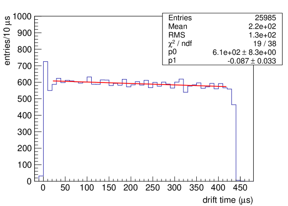
The number of hits in each time bin () is proportional, e.g. in the -view, to and can be related to the electron drift velocity
| (3) |
Assuming that the track is straight, the slope is constant and hence is proportional to . The distribution in Figure 19 can therefore be interpreted to be the drift velocity as a function of the vertical coordinate . The drift velocity is constant when the drift field is uniform, i.e. any deviation from a flat distribution indicates a non-uniformity of the field.
The excess at s is an edge effect which can be explained by the strong extraction field near the liquid argon surface. The rest of the distribution is straight and can be fitted with a line of a given slope to take into account the slight decrease towards a longer drift time, i.e. towards the bottom of the field cage. Fitting from 20 to 420 s and using the average velocity mm/s, one obtained
| (4) |
with mm/s and mm/s2. The drift velocity at the bottom of the field cage thus was calculated to be mm/s which is 94% of .
From the obtained drift velocity one can derive the drift electric field using our polynomial function shown in Figure 17 (dotted curve). The electric field thus calculated was V/cm at the top of the field cage, respectively V/cm at the bottom. The field at the bottom was found to be ()% smaller with respect to that at the top. For the first approximation this reduction of the electric field at the bottom of the field cage can be explained by the the non-linearity of the voltage distribution to the field shapers due to the shunt capacitance in the Greinacher circuit, as described in Section 3.4. The obtained reduction was found compatible with that of 10% which was expected for the shunt capacitance of 4.4 pF obtained from the measurement in LAr. It should be noted that such a non-linearity and its influence to the field uniformity can be reduced by further optimizations of the design of the Greinacher circuit and of the field cage, respectively. It can also be corrected for offline. The result reported above demonstrate that this method was effective in evaluating the uniformity of the drift field. With increased statistics it will allow a precise correction in the conversion of the measured drift time to -coordinate.
5 Conclusions
We have built and operated the first ever LAr LEM-TPC having a large active area with dimensions 76 40 cm2 and a drift length of 60 cm. The chamber was equipped with a 30-stage immersed cryogenic Greinacher HV multiplier for generating a HV for the drift field. The characteristics of the HV system were extensively studied in air at room temperature and in LAr. An acceptable linearity of the output DC voltage to the input AC voltage and of the voltage distribution over the Greinacher stages was obtained from the measurements. The LAr LEM-TPC prototype operated successfully in the double-phase (liquid-vapor) mode in pure argon during a test period of 1 month, recording three-dimensional images of very high visual quality from cosmic muon tracks. The HV system operated stably in the double-phase operation mode of the whole TPC in pure argon. As expected the system did not introduce noise problems on the readout electronics of the charge readout system, which is one of the advantages of this novel technique promising for a giant-scale LAr-TPC. The cathode voltage of 36 kV was reached leading to a drift field of 0.6 V/cm.
Acknowledgements.
This work was supported by ETH Zürich and the Swiss National Science Foundation (SNF). We are grateful to CERN for their hospitality and thank R. Oliveira and the TS/DEM group, where several of the components of our detector were manufactured. We also thank the RD51 Collaboration for useful discussions and suggestions. Special thanks go to N. Bourgeois and the CERN PLC support group for the PLC system and to T. Schneider and Thin Film & Glass group of CERN for helping us for the WLS coating of the PMTs. We thank Maria de Prado (CIEMAT), Takasumi Maruyama (KEK/IPNS), Junji Naganoma (Waseda), Hayato Okamoto (Waseda) for their participation in the data-taking phase.References
- [1] A. Badertscher et al., “First operation of a double phase LAr Large Electron Multiplier Time Projection Chamber with a two-dimensional projective readout anode,” Nucl. Instrum. Meth. A 641 (2011) 48 [arXiv:1012.0483 [physics.ins-det]].
- [2] A. Badertscher et al., “Operation of a double-phase pure argon Large Electron Multiplier Time Projection Chamber: Comparison of single and double phase operation,” Nucl. Instrum. Meth. A 617 (2010) 188 [arXiv:0907.2944 [physics.ins-det]].
- [3] S. Amerio et al. [ICARUS Collaboration], “Design, construction and tests of the ICARUS T600 detector,” Nucl. Instrum. Meth. A 527, 329 (2004).
- [4] C. Anderson et al. [ArgoNeuT Collaboration], “First Measurements of Inclusive Muon Neutrino Charged Current Differential Cross Sections on Argon,” arXiv:1111.0103 [hep-ex].
- [5] O. Araoka, A. Badertscher, A. Curioni, S. DiLuise, U. Degunda, L. Epprecht, L. Esposito and A. Gendotti et al., “A tagged low-momentum kaon test-beam exposure with a 250L LAr TPC (J-PARC T32),” J. Phys. Conf. Ser. 308, 012008 (2011) [arXiv:1105.5818 [physics.ins-det]].
- [6] A. Rubbia, “Experiments for CP violation: A Giant liquid argon scintillation, Cerenkov and charge imaging experiment?,” hep-ph/0402110.
- [7] A. Rubbia, “Underground Neutrino Detectors for Particle and Astroparticle Science: The Giant Liquid Argon Charge Imaging ExpeRiment (GLACIER),” J. Phys. Conf. Ser. 171 (2009) 012020 [arXiv:0908.1286 [hep-ph]].
- [8] A. Badertscher et al., “Giant Liquid Argon Observatory for Proton Decay, Neutrino Astrophysics and CP-violation in the Lepton Sector (GLACIER),” arXiv:1001.0076 [physics.ins-det].
- [9] A. Rubbia, “ArDM: A Ton-scale liquid Argon experiment for direct detection of dark matter in the universe,” J. Phys. Conf. Ser. 39 (2006) 129 [hep-ph/0510320].
- [10] A. Badertscher et al.. “First operation and performance study of a large area double phase LAr Electron Multiplier Time Projection Chamber and its dedicated readout electronic.”, in preparation.
- [11] H. Greinacher, “Über eine Methode, Wechselstrom mittels elektrischer Ventile und Kondensatoren in hochgespannten Gleichstrom umzuwandeln,” Z. Physik 4 (1921) 195.
- [12] J. D. Cockcroft and E. T. S. Walton, “Experiments with High Velocity Positive Ions. – (I) Further Developments in the method of obtaining High Velocity Positive Ions,” Proc. Roy. Soc. (London) 131 (1932) 619.
- [13] S. Horikawa et al., “Feasibility of high-voltage systems for a very long drift in liquid argon TPCs,” J. Phys. Conf. Ser. 308 (2011) 012027 [arXiv:1009.4908 [physics.ins-det]].
- [14] A. Marchionni et al. [ArDM Collaboration], “ArDM: a ton-scale LAr detector for direct Dark Matter searches,” J. Phys. Conf. Ser. 308 (2011) 012006 [arXiv:1012.5967 [physics.ins-det]].
- [15] C. M. B. Monteiro et al., “Secondary scintillation yield in pure argon,” Phys. Lett. B 668 (2008) 167.
- [16] R. Acciarri et al., “Demonstration and Comparison of Operation of Photomultiplier Tubes at Liquid Argon Temperature,” JINST 7 (2012) P01016 [arXiv:1108.5584 [physics.ins-det]].
- [17] V. Boccone et al. [ArDM Collaboration], “Development of wavelength shifter coated reflectors for the ArDM argon dark matter detector,” JINST 4 (2009) P06001 [arXiv:0904.0246 [physics.ins-det]].
- [18] E. Buckley et al., “A Study Of Ionization Electrons Drifting Over Large Distances In Liquid Argon,” Nucl. Instrum. Meth. A 275 (1989) 364.
- [19] M. M. Weiner, “Analysis of Cockcroft-Walton Voltage Multipliers with an Arbitrary Number of Stages” Rev. Sci. Instrum. 40 (1969) 330.
- [20] E. Everhart and P. Lorrain, “The Cockcroft-Walton Voltage Multiplier Circuit” Rev. Sci. Instrum. 24 (1953) 221.
- [21] L.Kaufmann, “Detector Performance and Background Studies for the ArDM Experiment”, PhD thesis ETH Nr. 17806.
- [22] D. A. Hill and M. Kanda, “Electric Field Strength,” The measurement, instrumentation, and sensors handbook XXV, Chapter 47, CRC Press and IEEE Press, 1999.
- [23] S. Amoruso et al. [ICARUS Collaboration], “Study of electron recombination in liquid argon with the ICARUS TPC,” Nucl. Instrum. Meth. A 523 (2004) 275.
- [24] W. Walkowiak, “Drift velocity of free electrons in liquid argon,” Nucl. Instrum. Meth. A 449 (2000) 288.