Suppression of Conductance in a Topological Insulator Nanostep Junction
Abstract
We investigate quantum transport via surface states in a nanostep junction on the surface of a 3D topological insulator that involves two different side surfaces. We calculate the conductance across the junction within the scattering matrix formalism and find that as the bias voltage is increased, the conductance of the nanostep junction is suppressed by a universal factor of 1/3 compared to the conductance of a similar planar junction based on a single surface of a topological insulator. We also calculate and analyze the Fano factor of the nanostep junction and predict that the Fano factor saturates at , five times smaller than for a Poisson process.
pacs:
73.20.-r, 73.23.-b, 73.40.-cExperimental demonstration of topological phases in both two-dimensional (such as HgTe) and three-dimensional (such as Bi2Se3) compounds with strong spin-orbit interaction Konig2007 ; Hsieh2008 ; Xia2009a ; Xia2009b has generated a plethora of interest in the physics community Hasan2010 . These compounds are insulating in the bulk (since they have an energy gap between the conduction band and the valence band) but their surfaces support gapless topological excitations. These surface states are topologically protected against non-magnetic defects by time-reversal symmetry Hasan2010 .
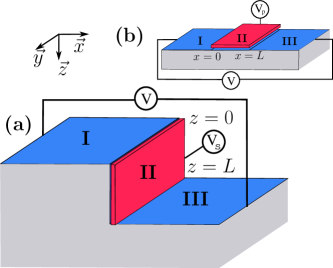
In the simplest case these low-energy excitations of a strong three-dimensional (3D) topological insulator can be described by a single Dirac cone at the center of the two-dimensional Brillouin zone ( point) Konig2007 ; Xia2009a ; Hasan2010 . Recently, naturally occurring defects such as step-like imperfections Seo2010 ; Alpichshev2010 have been studied in the context of topological insulators. Conductance through atomic scale step-defects has been measured demonstrating that the surface states are protected in spite of such an abrupt defect Seo2010 . These atomic sized steps are usually modeled as delta function potential barriers StepDefects . In this article we investigate quantum transport through a nanostep junction involving two different side surfaces of a 3D topological insulator. We predict that the conductance of the nanostep junction is suppressed in the large-energy limit by a universal factor of 1/3 as compared to the conductance of a similar junction based on a single surface of a 3D topological insulator (or a similar junction in graphene). Figure 1(a) shows a schematic of the nanostep junction considered. The junction is divided into three regions. In region I ( and ) and in region III ( and ) the surface states lie in the - plane, while in region II ( and ) the surface states lie in the - plane. A dc bias voltage is applied between region I and III and a top gate controls the carriers in region II. Figure 1(b) shows a schematic of the analogous planar junction, where in all three regions the surface states lie in the - plane and a top gate is applied to region II. The first junction [Fig. 1(a)] is referred to as a step junction, and the second junction [Fig. 1(b)] as a planar junction in the rest of this article. We use the conceptually transparent scattering matrix formalism to calculate the transport properties of these junctions yuli . For concreteness, we use typical parameter values of the 3D topological insulator Bi2Se3 when illustrating our results.
The low-energy effective Hamiltonian for Bi2Se3 in the basis of four hybridized states of Se and Bi -orbitals denoted as , , , can be written as wen2010 :
| (1) |
where , , , and parameters . Here stands for up (down) spin and stands for even (odd) parity. From this three-dimensional Hamiltonian, there exists a straightforward procedure to obtain the effective Hamiltonian describing the surface states Qui2011 ; wen2010 . The surface states in the - plane, for example, are obtained from the three-dimensional wavefunctions for these surface states (which are exponentially damped in the -direction, with finite skin depth ) using Eq. (1), followed by imposing the boundary conditions of vanishing wavefunctions at the two boundaries ( and ). For three-dimensional topological insulators () the surface states at the two boundaries are decoupled and the effective Hamiltonian describing the carriers in regions I and III is then given by Qui2011 :
| (2) |
where , represents the Fermi velocity in the - plane and and denote the usual Pauli matrices.
Analogously, we obtain the effective Hamiltonian describing the carriers in region II as
| (3) |
where and . Solving the Hamiltonian (2), we obtain the eigenstates in region I and region III as
| (6) |
with corresponding energy eigenvalues given by and . Similarly, in region II we obtain:
| (9) |
with corresponding energy eigenvalues and . The labels of the wavefunction indicate right (left) traveling carriers in regions I and III, and downwards (upwards) traveling carriers in region II. It should be noted that in general , which implies that the Dirac cone describing the surface states in the - plane is shifted by an energy of with respect to the Dirac cone describing surface states in the - plane. Furthermore, the Dirac cone describing the excitations in region II has elliptic cross section (). These features are in good agreement with recent electronic structure calculations of similar systems Moon2011 .
Considering electrons incident from left to right, the total wavefunction in the different regions can be written as:
| (10) |
The reflection and transmission coefficients and can be obtained by imposing the boundary conditions under which the current normal to the boundary is conserved BoundaryGraphene ; Sen2012 ; boundary . We then find for the transmission probability of an electron incident on the step junction at a given angle of incidence :
| (11) |
with
| (12) |
and . Eq. (12) is obtained by using conservation of energy and conservation of momentum along the -direction.
The zero-temperature conductance across the step junction is then given by yuli :
| (13) |
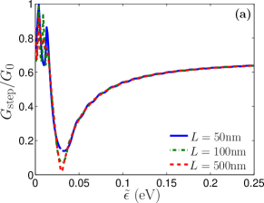
Here , denotes the density of states, the sample width, and the integration is over all angles of incidence . Figure 2(a) shows the conductance [Eq. (13)] as a function of energy for different values of . We observe that the conductance reaches a minimum at , arising from the difference in Dirac point energies in different planes. Beyond this point, the conductance first oscillates and then saturates at large energies. For the conductance reaches a limiting value of 2/3, independent of barrier width . Below (see Eq. (15)) we discuss the behavior of the conductance close to this saturation point in more detail.
The transmission probability of the analogous planar junction [see Fig. 1(b)] with a top gate in the middle region is given by vBarrierGraphene :
| (14) |
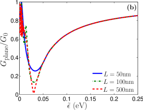
Here represents the -component of the momentum in region II, the energy dispersion is given by and . Figure 2(b) shows the conductance as a function of energy for different values of . As before, the conductance reaches a minimum when , and then increases to reach its saturation value . For larger energies, the conductance of the step junction is thus suppressed by a factor of 1/3 compared with planar junctions. We attribute this suppression to the fact that the carriers in the step junction have to change their plane of propagation in region II spinorbit .
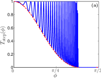
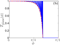
We now analyze in more detail the difference between the conductance of the step and the planar junction by comparing the denominators in Eqns. (11) and (14). Figure 3 shows the transmission probabilities and as a function of the angle of incidence . From Fig. 3(a) we see that for the step junction there is a cut-off angle of incidence, which arises from the finite energy and velocity mismatch. This critical angle can be expressed as . We also see that the conductance of both junctions includes contributions from many resonant modes. Here, a resonant mode is defined as a mode with an angle of incidence for which the transmission . The various minima of these resonant modes form an envelope, as shown by the dashed (red) lines in Fig. 3. These envelope functions are obtained from the transmission expressions Eqns. (11) and (14) by setting and , respectively, with integer. When the number of resonant modes is large () a lower bound for the integrated transmission is obtained by integrating over the envelope function. Under these conditions the conductance of the step junction [Eq. (13)] becomes
| (15) | |||||
Similarly, we find for the planar junction
| (16) |
where . The suppression of the conductance in the vicinity of the saturation value thus depends on the shift of the Dirac point energies and the ratio of the Fermi velocities in region I and II exactbound . As final remarks, we note that the effect of the elliptical dispersion in the middle region of the step junction can be incorporated as an effectively wider barrier, and , compared to the planar junction. The minimum barrier width needed to observe the suppression in the conductance described above is given by the condition for the existence of the first resonant mode in the junction, . In the case of Bi2Se3, this minimum width is nm. For cleaved topological insulators, widths of nm have been reported GZhang2009 .
In the remaining part of this paper we investigate the Fano factor of the step junction, which is a measure for the noise suppression in the junction relative to Poisson noise yuli . Within the scattering matrix formalism the Fano factor is defined as
| (17) |
where is the angle of incidence of the carriers and represents the transmission of the junction. Substituting Eqns. (11) and (14) into Eq. (17) and evaluating the integrals in general leads to lengthy expressions. However, in the limit of a large number of resonant modes () we find that the Fano factor of the step junction is given by approx
| (18) |
where as defined earlier.
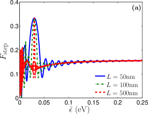
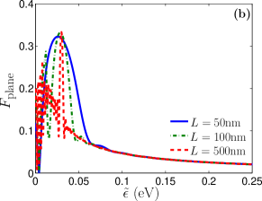
Figure 4 shows the calculated F and F for different values of the junction width L. As the energy of the incident carriers increases, both Fano factors reach a maximum around eV, where and respectively. For higher energies the Fano factor of the step junction oscillates around its saturation value , which is five times smaller than the Fano factor expected for a Poisson process, . On the other hand, the Fano factor F for the planar junction vanishes as the energy of the incident carriers increases. This can be explained by noticing that the transmission T as increases (see Fig. 2(b)). This remarkable difference in the Fano factor for the two junctions again suggests that there exists an additional scattering mechanism for the step junction that does not exist in the planar junction, namely the change of plane of propagation of the topological surface states.
In conclusion, we have proposed and analyzed quantum transport through a nanostep junction on the surface of a 3D topological insulator in the ballistic limit. Our results show that the conductance in a nanostep junction is suppressed by up to a factor of 1/3 compared to similar junctions based on a single surface of a 3D topological insulator or graphene. Although the suppression depends on the ratio of the Fermi velocities and the difference in Dirac point energies of the different side surfaces of the 3D topological insulator, the saturation values of the conductance and Fano factor themselves G and F are universal. We also predict oscillating behavior of the Fano factor around its saturation value. Experimental demonstration DiCarlo2008 of our predictions will provide further insight into the scattering mechanisms involved in topological insulator nanostep junctions.
We would like to thank C. Bruder for valuable discussions. This research was supported by the Dutch Science Foundation NWO/FOM. RPT acknowledges financial support by the Swiss SNF, the NCCR Nanoscience, and the NCCR Quantum Science and Technology.
References
- (1) M. König et al., Science 318, 766 (2007).
- (2) D. Hsieh et al., Nature 452, 970 (2008).
- (3) Y. Xia et al., Nature Phys. 5, 398 (2009).
- (4) Y. Xia et al., arXiv:0907.3089.
- (5) M. Z. Hasan and C. L. Kane, Rev. Mod. Phys. 82, 3045 (2010).
- (6) J. Seo et al., Nature 466, 343 (2010).
- (7) Z. Alpichshev et al., Phys. Rev. Lett. 104, 016401 (2010).
- (8) R. R. Biswas, and A. V. Balatsky, Phys. Rev. B 83, 075439 (2011); D. Zhang and C. S. Ting, ibid. 85, 115434 (2012).
- (9) Y. V. Nazarov and Y. M. Blanter, Quantum Transport: Introduction to Nanoscience (Cambridge University Press, Cambridge, UK, 2009).
- (10) The parameters , , , , , , , and can be determined by fitting the energy spectrum of the effective Hamiltonian (1) with that of ab initio calculations, see H. Zhang et al., Nature Physics 5, 438 (2009).
- (11) W.-Y. Shan, H.-Z. Lu, and S.-Q. Shen, New J. Phys. 12, 043048 (2010).
- (12) X.-L. Qui and S.-C. Zhang, Rev. Mod. Phys. 83, 1057 (2011).
- (13) C.-Y. Moon, J. Han, H. Lee, and H. J. Choi, Phys. Rev. B 84, 195425 (2011).
- (14) E. McCann and V. I. Falko, J. Phys. Cond. Matt. 16, 2371 (2004); A. R. Akhmerov and C. W. J. Beenakker, Phys. Rev. B 77, 085423 (2008).
- (15) D. Sen and O. Deb, arXiv:1203.3347.
- (16) Notice that in our case the current normal to the junction has and -components and boundary conditions are given by and .
- (17) R. Arnaud et al., Phys. Rev. B 81, 073407 (2010); A. Concha, and Z. Tešanović, ibid. 82, 033413 (2010).
- (18) For topological insulators with strong spin orbit interactions, a change in the plane of propagation is accompanied by a change in the spin due to the helical nature of the surface states. Although our model does not take spin explicitly into account, it is implicitly included in the Hamiltonian (1).
- (19) Note that the lower bound Eq. (15) becomes exact in the limit .
- (20) G. Zhang et al. Appl. Phys. Lett. 95, 053114 (2009).
- (21) Note that the approximation gives a lower bound on the conductance and an upper bound on the Fano factor.
- (22) As has been done for shot noise in graphene, see e.g. L. DiCarlo et al., Phys. Rev. Lett. 100, 156801 (2008).