Preparation of an Exponentially Rising Optical Pulse for Efficient Excitation of Single Atoms in Free Space
Abstract
We report on a simple method to prepare optical pulses with exponentially rising envelope on the time scale of a few ns. The scheme is based on the exponential transfer function of a fast transistor, which generates an exponentially rising envelope that is transferred first on a radio frequency carrier, and then on a coherent cw laser beam with an electro-optical phase modulator (EOM). The temporally shaped sideband is then extracted with an optical resonator and can be used to efficiently excite a single 87Rb atom.
pacs:
37.10.Gh, 42.50.Ct, 32.90.+aI Introduction
In recent years there has been significant progress towards establishing an efficient quantum interface between photons and atoms. Such an interface is commonly considered as a building block for complex quantum network circuits where atoms exchange information (photons) via fundamental processes of absorption and emission Luo et al. (2009); Cirac and Zoller (2004); Cirac et al. (1997). For this processes to be efficient without any field enhancement by cavity structures, there should be a significant overlap between atomic and photonic modes in spatial and time-frequency domains. In other words, the photons must be spatially and temporarily “shaped” to match the properties of atomic (electric dipole) transitions Sondermann et al. (2007); Stobińska et al. (2009); Wang et al. (2011).
For the spatial matching, the spatial profile of atomic absorption/emission pattern is approximated by an oscillating (rotating) electric dipole, corresponding to () transitions. An almost perfect spatial overlap of light with a transition can be achieved with a radially polarized light focused by parabolic mirror to an atom Sondermann et al. (2007). However, a significant spatial overlap between a Gaussian mode and transitions can already be accomplished by focusing with commercially available high numerical aperture lenses Tey et al. (2009).
For the temporal matching, a simple argument suggests that the time-reversal of a spontaneous emission process as described by Weisskopf and Wigner, namely an exponentially rising electrical field strength, should yield a high excitation probability. It was shown in a few recent theoretical articles that that for a given spatial overlap the highest excitation probability of an atom occurs for photons with an exponentially rising envelope that is terminated by a sharp drop Stobińska et al. (2009); Wang et al. (2011).
A straight-forward approach to generate coherent light pulses with an adequate temporal shape uses some sort of optical modulator for a cw light beam, and some electronic way to prepare an envelope signal that has an exponential rise time on the order of a few nsec. While an exponentially decaying envelope signal on this time scale is very simple to prepare e.g. by a RC low pass filter, an exponential rising envelope is slightly more difficult. While these days arbitrary function generators for analog signals have just about become fast enough to implement this directly, we present a much simpler method in this paper.
II Implementation

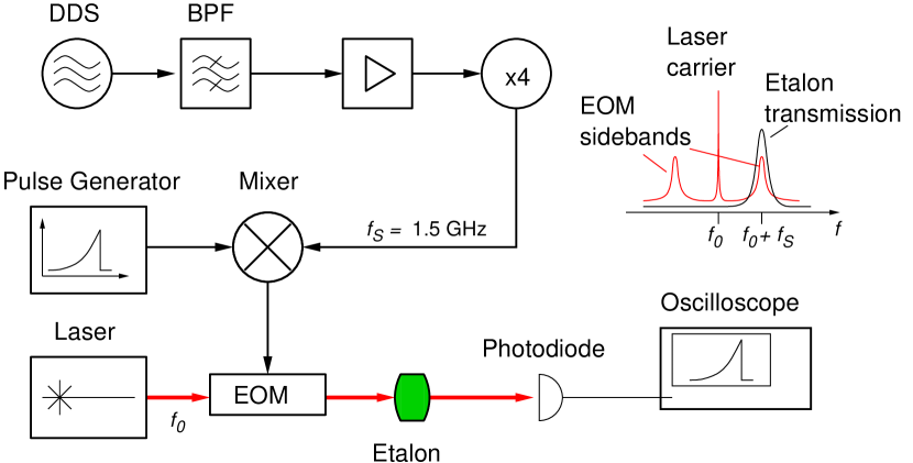
An overview of our experimental setup is shown in FIG 1. The core idea is to use the transfer function of a transistor to convert a linear rising electrical signal into an exponentially rising current. With this current, we first modulate the envelope of a radio frequency carrier, which is then used in an electro-optical phase modulator (EOM) to imprint optical side bands onto a coherent, frequency-stabilized cw laser beam. An etalon is used to filter out one of the sidebands with enough bandwidth to recover the exponential shape in time, and sent to a fast photodiode for characterization. In the following, we describe the various building blocks in more detail.
II.1 Electrical pulse
The collector current of an unsaturated bipolar junction transistor depends on its base voltage according Shockley relationship:
| (1) |
where is the reverse saturation current and mV at room temperature. If increases linearly in time, the collector current grows in good approximation exponentially if . Figure 2 shows the electrical circuit that implements this idea, together with other components ensuring a fast switch-off. The design time constant for the exponential rise was about 27 ns to match the decay time of the optical transition on a D2 line in Rubidium.

A linearly rising is provided by charging capacitor C1 with a constant current . Transistor T1 then performs the transformation of the linear slope into an exponentially rising current . For the nominal ns a slope V/s is necessary. For C1=3.9 nF, this slope can be accomplished with a reasonable charging current mA.
The charge current is provided by the current source combination T7 and R11, which generates a current defined by an analog input voltage , and allows for a variation of by a factor of about 5 in both directions for exploring different interaction regimes of the optical pulse with the atom. The exponential time constant of the output pulse is then roughly given by
| (2) |
The desired pulse has not only an exponential rise, but also a steep cutoff at a given time, and the whole shape of the pulse needs to be defined with respect to some external timing reference. For this purpose, we use a digital signal following a NIM standard suitable to interact with our control equipment. This timing signal starts the charging of C1 when active ( V), and routes the the output current via T2 into the load impedance. When switching to passive state ( V), the output current is diverted through T3 away from the output, and C1 is discharged via T4. The basis voltage levels of T2,T3 are chosen such that the main transistor T1 has a collector potential of 3.7…4.2 V to keep it unsaturated. T2 and T3 themselves stay out of saturation for an output voltage up to 2V corresponding to mA.
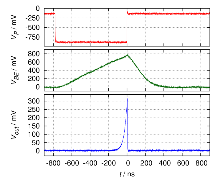
The timing of the pulse is now critically determined by the length of the control pulse , and critically dependent on the temperature voltage as well. A timing diagram of the relevant voltages for a typical time constant of 30.5 ns is shown in figure 3.

II.2 RF generation and mixing
In the experiment, the resulting optical frequency of the pulse has to be tuned across the closed cycling transition of which occurs between hyperfine states of D2 line at THz. The RF carrier at frequency that is modulated with the exponential envelope signal defines the splitting between the optical carrier frequency of the laser and the sidebands that are obtained with EOM. We choose GHz, because in this case, hits the transition frequency of D2 line in between and , and the laser carrier frequency can be locked to a vapor cell containing the natural isotope distribution of Rb.
The RF carrier is prepared by a direct digital synthesizer (DDS) based on an Analog Devices AD9958 chip, running at a sampling frequency of 500 MHz. From this, we reconstruct the first upper mirror frequency at 375 MHz with a strip line band pass filter (spurious suppression: 70 dBc at 125 MHz, 24 dBc at 500 MHz, 35 dBc at 625 MHz). After an amplification to about 0 dbm this carrier is twice frequency-doubled (Mini-circuits AMK2-13 and KC2-11) to the desired GHz, and used as a local oscillator input of a double-balanced mixer (Mini-circuits ADE-30). The attenuated envelope signal is connected to the IF port of the mixer.

II.3 EOM and filter cavities
The modulated RF signal around is converted into an optical sideband with a waveguide electro-optical phase modulator (EOSpace, model PM-0K5-10-PFA-PFA-780). It has an electrical bandwidth of nominally 20 GHz and a half wave voltage mV. Since the amplitude of the optical side band is proportional to , where is the Bessel function and the amplitude of the radio frequency signal, must be kept low enough to minimize distortion of the amplitude transfer due to the nonlinearity of the Bessel function. For , the distortion is about 1.2%, for already 4.8%.
In a next step, one of the optical side bands needs to be isolated from the optical carrier and the other sideband. We do this with an etalon that is formed by a plano-convex fused silica substrate with a radius of curvature of mm and a center thickness of 6.35 mm. Both surfaces of this lens substrate are coated with dielectric mirrors with a reflectivity of 95%, leading to a free spectral range of about 17 GHz and a transmission line width (FWHM) of 273 MHz. This solid etalon can be temperature-tuned to transmit one optical sideband, with a temperature tuning of 7.4 K for one full spectral range of 17 GHz. We keep the temperature stable to about 5 mK, resulting in a frequency uncertainty of 11.5 MHz. For the given etalon reflectivity, there is still a transmission of 0.77% at the optical carrier frequency. We thus use three consecutive etalons to achieve more than 60 dB carrier power extinction.
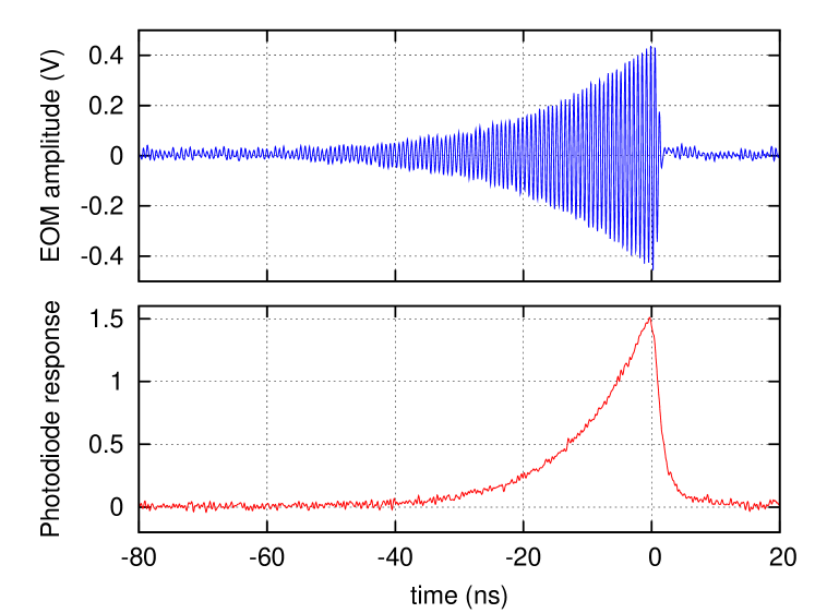
A quick characterization of the emerging pulse was carried out with a fast PIN silicon photodiode (Hamamatsu S5973, nominal bandwidth 1 GHz) connected to a oscilloscope with 2 GHz bandwidth (see FIG 4). While the RF signal sent to the EOM shows an exponentially rising envelope with a time constant of about 17.4 ns, the optical pulse seen by the photodiode shows a rise with a time constant of about 10 ns. The time constants should differ by a factor of 2 exactly due to the square dependency of the optical power sensed by the photodiode from the electrical field amplitude. Compared to the sudden drop in the modulated RF signal, the optical response also shows a slower decay. This is partly due to the finite bandwidth of the filter cavities, which induces a ringdown time of the triple cavity system, and partly due to the photodiode response. To realize a faster stop of the optical wave packet, one would need to choose a larger filter cavity bandwidth, and consequently a larger RF carrier frequency.
III Summary
We presented a very simple scheme to generate a fourier-limited optical pulse with an exponentially rising amplitude and a sharp decay from a cw laser tuned to a resonance of an atomic transition. For a large overlap of the spatial mode of such a light field with the emission pattern of a dipole transition, such a pulse should lead to high excitation probability of an atom (or any other two-level system) with a small average photon number.
References
- Luo et al. (2009) I. L. Luo, D. Hayes, T. A. Hanning, D. N. Matsukevich, P. Maunz, S. Olmschenk, J. D. Sterk, and C. Monroe, Fortschritte der Physik 57, 1133 (2009).
- Cirac and Zoller (2004) J. I. Cirac and P. Zoller, Physics Today 57, 38 (2004).
- Cirac et al. (1997) J. I. Cirac, P. Zoller, H. J. Kimble, and H. Mabuchi, Phys. Rev. Lett. 78, 3221 (1997).
- Sondermann et al. (2007) M. Sondermann, R. Maiwald, H. Konermann, N. Lindlein, U. Peschel, and G. Leuchs, Appl. Phys. B 89, 489 (2007).
- Stobińska et al. (2009) M. Stobińska, G. Alber, and G. Leuchs, Europhys. Lett. 86, 14007 (2009). URL http://arxiv.org/abs/0808.1666v2.
- Wang et al. (2011) Y. Wang, J. Minar, L. Sheridan, and V. Scarani, Phys. Rev. A 83, 063842 (2011).
- Tey et al. (2009) M. K. Tey, S. A. Aljunid, F. Huber, B. Chng, Z. Chen, G. Maslennikov, and C. Kurtsiefer, New Journal of Physics 11, 043011 (2009).