The structural and electronic properties of tin oxide nanowires: an ab initio investigation
Abstract
We performed an ab initio investigation on the properties of rutile tin oxide (SnOx) nanowires. We computed the wire properties determining the equilibrium geometries, binding energies and electronic band structures for several wire dimensions and surface facet configurations. The results allowed to establish scaling laws for the structural properties, in terms of the nanowire perimeters. The results also showed that the surface states control most of the electronic properties of the nanowires. Oxygen incorporation in the nanowire surfaces passivated the surface-related electronic states, and the resulting quantum properties and scaling laws were fully consistent with electrons confined inside the nanowire. Additionally, oxygen incorporation in the wire surfaces generated an unbalanced concentration of spin up and down electrons, leading to magnetic states for the nanowires.
Escola Politécnica, Universidade de São Paulo, CP 61548, CEP 05424-970, São Paulo, SP, Brazil] Universidade de São Paulo, São Paulo, SP, Brazil Instituto de Física,Universidade de São Paulo, CP 66318, CEP 05315-970, São Paulo, SP, Brazil] Escola Politécnica, Universidade de São Paulo, CP 61548, CEP 05424-970, São Paulo, SP, Brazil] Universidade de São Paulo, São Paulo, SP, Brazil
1 Introduction
Over the last decade, there has been growing interest in semiconducting one-dimensional nanostructures 1, 2. They open possibilities for quantum confinement, which may allow to obtain tailored electronic properties, such as optical transitions in pre-determined wavelengths and selective electronic response from interaction with specific molecules 3. Among many semiconducting nanostructured materials, tin oxide (SnOx) nanowires have received special attention, mostly due to several promising applications, such as gas 4, 5, chemical 6 and humidity 10 sensors, solar cells 7, optical devices 8, 9, and high-density batteries 11, 12. For sensors, nanostructured tin oxide represents an improvement over the previous devices based on bulk tin oxide, since they provide greater surface/volume ratio, allowing to get higher sensitivity and selectivity for several chemical species.
Tin oxide nanowires have been grown, in rutile configuration, along the [001] 13, [011] 12, [101] 16, 17, 14, 15, and [121] 15 directions. Nanostructured tin oxide have also been recently grown in other forms, such as nanotubes 16, nanoribbons 19, and nanorods 18. Those one-dimensional nanostructures have been synthesized by several processes, such as wet-chemical approach 13, high temperature thermal oxide 16, hydrothermal 17 and vapor-liquid-solid 14 methods, carbothermal reduction 15, plasma-enhanced chemical vapor deposition 18, and through oxidation of tin vapors at elevated temperatures 19.
Square-shaped rutile tin oxide nanowires, along the [001] direction, have been obtained with diameters of around 80 nm and lengths of a few micrometers 13. Tin oxide nanowires with rectangular cross sections have also been grown along the [101] direction, leading to structures with diameters of 50-150 nm and lengths of around 10-100 m. Those results indicate very large length/diameter ratios, which may be important for incorporation in integrated circuits.
There are several questions that still need to be addressed to optimize the use of tin oxide nanowires as nanosensors 20. For example, several sensing properties require attention, such as the response time, sensitivity, selectivity, and degradation to long-term exposure to gases. In order to optimize the sensing performance, it is important to understand the fundamental properties of those tin oxide nanowires, and how those properties scale. Here, we explored the electronic and structural properties of rutile [100] SnOx nanowires, with several facet configurations, using simulations based on first-principles total energy methodologies. We observed that the scaling laws of the structural properties could be described in terms of the amount of nanowire surface, independent of the wire shape, which is expressed in terms of the nanowire perimeter, consistent with what was observed for nanowires of different materials 27, 28. We also showed that the electronic properties of the nanowires are strongly affected by the oxygen passivation of surface states. Additionally, we observed that such passivations lead to magnetic states for the nanowires.
2 Methodology
Although the sensing properties and the growth procedures of tin oxide nanowires have been intensively studied, there is scarce literature that covers the theoretical modeling of this material. The electronic quantum confinement in tin oxide nanowires, with artificial surface passivation, have been investigated within the density functional theory 21. That investigation showed that the wire bandgap scales with the inverse of the wire diameter, since the surface-related energy levels were fully removed by the surface passivation. On the other hand, there are similarities on the structural properties of tin oxide and titanium oxide nanowires, such that their properties are general compared by theoretical investigations. In the case of titanium oxide nanowires, there is a more extensive literature, that covers the theoretical investigations on their structural and electronic properties 22, 23, 24, 25, 26.
Our calculations on tin oxide nanowires were performed using the Vienna ab initio simulation package (VASP) 29. The electronic exchange-correlation potential was described within the spin-polarized density functional theory and the generalized gradient approximation (DFT-GGA) 30. The electronic wave-functions were described by a projector augmented wave (PAW) method 31, taking a plane-wave basis set with a kinetic energy cutoff of 400 eV. Self-consistent calculations were performed until reaching convergence in total energy of 1 meV between two consecutive iterations. Configurational optimization was performed by considering relaxation in all atoms, without any symmetry constrain, until forces were smaller than 3 meV/Å in any atom. The Brillouin zone was sampled by a k-point grid 32. The structures were built using periodic boundary conditions with a tetragonal simulation cell. In the directions perpendicular to the nanowire one (), lattice parameters were chosen such that there was a large open space between the atoms in the original cell and those in the image ones. We found that an open space of about 15 Å in any direction was large enough to prevent interactions between the atoms in the simulation cell with those in the neighboring image cells.
3 Results
Tin dioxide (SnO2) in a crystalline bulk phase has a tetragonal structure with the space group (P4/mnm, 136), with experimental 33 (calculated) lattice parameters Å Å, , resulting in Sn-O average interatomic distance of 2.054 (2.094) Å. Bulk tin oxide is a wide band gap (Eg=3.6 eV) metal oxide semiconductor, as measured by optical absorption 34. Our calculations for the bulk crystal gave a value of 0.65 eV for the direct band gap at the point. Our results in terms of interatomic distances and bandgap were in good agreement with other theoretical investigations based on the density functional theory 35. Therefore, the present investigation also observed the general trend of DFT calculations to underestimate the bandgap of bulk SnO2 and DFT-GGA to overestimate the lattice parameters 36.
Tin oxide (SnOx) nanowires have been observed to grow in the rutile configuration, in several growing directions, but most of the investigations are associated with wires along the [001] direction. Additionally, due to the strong interatomic Sn-O interactions, those nanowires have a core that resembles the structure of their crystalline counterpart. Therefore, we focused our investigation on the properties of nanowires with a crystalline core grown along the [001] direction, and several facet configurations.
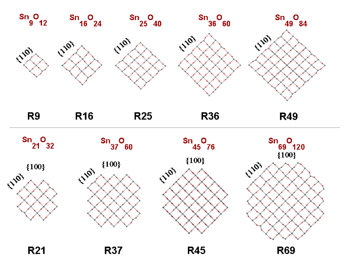
1 presents the cross section of the tin oxide nanowires investigated here. We initially considered the properties of nanowires without any surface passivation, only later we observed the role of oxygen passivation on the electronic properties of the wires. The figure represents the relaxed final configurations of the simulations for the nanowires with pure {110} surface facets (R9, R16, R25, R36, and R49) and with a mixture of {100} and {110} ones (R21, R37, R45, and R69). The results indicated that tin oxide nanowires keep their rutile-like structure even for the smallest dimensions, such as the nanowires with labels R9 and R21, with both types of surface configurations.
Determining scaling laws for the properties of nanowires has been a challenging task, mainly when trying to compare the properties of wires with different surface facets, or even with different growing directions. Several attempts to establish those scaling laws, in terms of the wire cross sections, diameter, or even density of atoms in the wire, have failed. The diameter is generally chosen as the dimensional parameter in which a scaling law is built 37, 38. However, defining a unique nanowire diameter is not simple, since those nanowires generally have facets and do not have a single diameter. Authors either avoid defining such a parameter 39, 37, or describe the wire representative dimension as the smallest wire diameter, taken from images of the wire cross section 38. Ultimately, it is generally assumed that the nanowires have a prevailing cylindrical shape 40, 41. For nanowires with large diameters ( 5nm), properties are generally well described using any of those assumptions, but for thinner wires those models clearly fail. As a result, the scaling laws in terms of those dimensional physical parameters are valid only within a specific wire family, in which all the wires have the same growth direction and surface types.
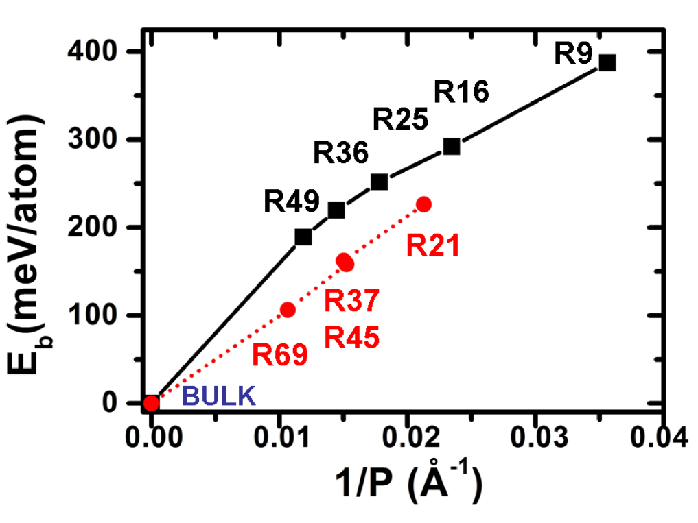
The literature lacks a unified model that could put together nanowires of a certain material with all types of surfaces, facets, and growth directions. Recently, interatomic potentials 42, 43 have been used to show that the nanowire scaling laws could be well described in terms of the respective wire perimeters 27, 28. The relevance of such dimensional parameter was not casual, the wire perimeter (P), the sum of all sides of the wire cross section, multiplied by the length of the wire (L) gives the total nanowire surface area (S = P L). It is well known that the ratio of surface/volume of nanowires is very large, such that the properties of those nanostructures would scale with the amount of nanowire surface ((S). 2 shows the binding energy of all the nanowires presented in 1. The figure presents the energy as a function of the inverse perimeter (1/P) of the nanowire. It gets clear that each family of wire type has an specific trend in energy, scaling with the inverse perimeter, all going to the same value for the bulk (as the perimeter tends to infinite).
The results showed that, for each family, there is an almost linear relation between binding energy and 1/P, for a wide range of wire perimeters. The trend only deviates from a linear behavior for very small nanowires (large 1/P), for example beyond the R16 wire. This is a reasonable result, considering that for those very thin nanowires, the strong rutile-like structure starts to weaken its rigidity and the systems relax toward more favorable configurations.
Table I summarizes the structural properties of all nanowires studied here. The Sn-O average interatomic distances, for thin nanowires, are larger than the value for the three-dimensional bulk SnO2 crystal. On the other hand, the Sn-O average interatomic distances, of those atoms sitting in the nanowire surface, remain much larger than the bulk value for all wires.
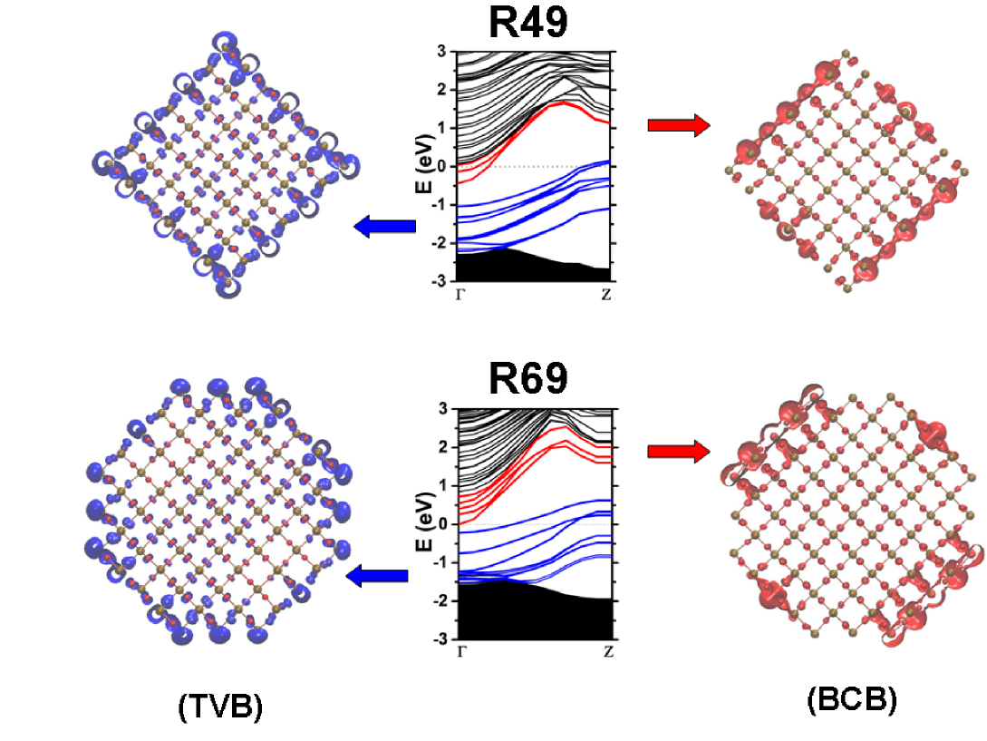
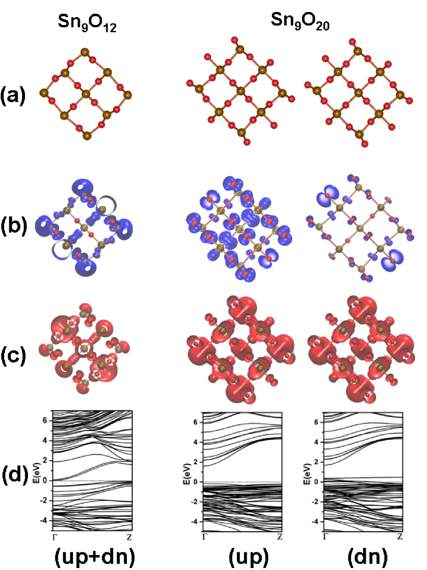
3 shows the electronic band structure of nanowires of the two families (R49 and R69), and their respective states near the top of the valence band and in the bottom of conduction band. It gets clear that the the surface states control the properties of the bandgap for excitations of both electrons and holes. 4 presents the effects of incorporating oxygen atoms in the surfaces of one of the nanowires (R9). First, for the unpassivated nanowire, there is a large number of states that stay in the nanowire bandgap, as observed in 3. As oxygen is introduced in the surface, those states are removed from the bandgap, as those states move toward the valence and conduction bands. Additionally, the incorporation of oxygen atoms in the surface generates an unbalanced distribution between up and down states, leading to a magnetic state. This result appears very appealing, since those wires could be used as devices based on spin polarized states.
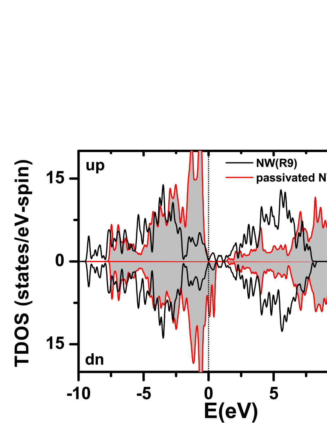
The oxygen passivation could be better understood in terms of the modifications in the electronic density of states upon passivation. 5 presents the density of stats for the R9 nanowire without and with oxygen passivation. Two main effects were observed. First, the oxygen passivation essentially moved the conduction bands upward, opening a bandgap. Second, it lead to a modification of the highest occupied energy levels, with important oxygen p-related levels in the top of the valence band. Those oxygen p-related levels are responsible for the resulting magnetic effects in the nanowires.
4 Summary
In summary, we carried a theoretical investigation on the structural and electronic properties of tin oxide nanowires. We found that the scaling laws of structural properties could be well described in terms of the nanowire perimeter. We also observed that the nanowires kept their rutile-like configurations even for the thinnest wires. In terms of the electronic structures, we found that the surface states control the bandgap states for unpassivated nanowires. Those surface-related states were fully passivated upon oxygen incorporation. The resulting nanowires presented non negligible spin polarization, coming from the p-related stated of the surface oxygen atoms.
Acknowledgments: The authors acknowledge partial support from Brazilian agencies FAPESP and CNPq.
References
- 1 Cui, Y.; Wei, Q. Q.; Park, H.K.; Lieber, C. M. Science 2001, 293, 1289.
- 2 Comini, E.; Baratto, C.; Faglia, G.; Ferroni, M.; Vomiero, A.; Sberveglieri, G. Prog. Mat. Sci. 2009, 54, 1.
- 3 Lu, W.; Lieber, C. M. J. Phys. D - Appl. Phys. 2006, 39, R387.
- 4 Kolmakov, A.; Zhang, Y.; Cheng, G.; Moskovits, M. Adv. Mater. 2003, 15, 997.
- 5 Kolmakov, A.; Klenov, D. O.; Lilach, Y.; Stemmer, S.; Moskovits, M. Nano Lett. 2005, 5, 667.
- 6 Sysoev, V. V.; Goschnick, J.; Schneider, T.; Strelcov, E.; Kolmakov, A. Nano Lett. 2007, 7, 3182.
- 7 Gubbala, S.; Chakrapani, V.; Kumar, V.; Sunkara, M. K. Adv. Funct. Mater. 2008, 18, 2411.
- 8 Luo, S.; Fan, J.; Liu, W.; Zhang, M.; Song, Z.; Lin, C.; Wu, X.; Chu, P. K. Nanotechnology 2006, 17, 1695.
- 9 Chen, R.; Xing, G. Z.; Gao, J.; Zhang, Z.; Wu, T.; Sun, H. D. Appl. Phys. Lett. 2009, 95, 061908.
- 10 Kuang, Q.; Lao, C.; Wang, Z. L.; Xie, Z.; Zheng, L. Journ. Am. Chem. Soc. 2007, 129, 6070.
- 11 Park, M.-S.; Wang, G.-X.; Kang, Y.-M.; Wexler, D.; Dou, S.-X.; Liu, H.-K. Angew. Chem. 2007, 119, 764.
- 12 Zhong, L.; Liu, X. H.; Wang, G. F.; Mao, S. X.; Huang, J. Y. Phys. Rev. Lett. 2011, 106, 248302.
- 13 Qin, L.; Xu, J.; Dong, X.; Pan, Q.; Cheng, Z.; Xiang, Q.; Li, F. Nanotechnology 2008, 19, 185705.
- 14 Kar, A.; Stroscio, M. A.; Meyyappan, M.; Gosztola, D. J.; Wiederrecht, G. P.; Dutta, M. Nanotechnology 2011, 22, 285709.
- 15 Phadungdhitidhada, S.; Thanasanvorakun, S.; Mangkorntong, P.; Choopun, S.; Mangkorntong, N.; Wongratanaphisan, D. Curr. Appl. Phys. 2011, 11, 1368.
- 16 Dai, Z. R.; Gole, J. L.; Stout, J. D.; Wang, Z. L. Journ. Phys. Chem. B 2002, 106, 1274.
- 17 Lupan, O.; Chow, L.; Chai, G.; Schulte, A.; Park, S.; Heinrich, H. Mater. Sci. Eng. B 2009, 157, 101.
- 18 Huang, H.; Gong, H.; Chow, C. L.; Guo, J.; White, T. J.; Tse, M. S.; Tan, O. K. Adv. Funct. Mater. 2011, 21, 2680.
- 19 Hu, J. Q.; Ma, X. L.; Shang, N. G.; Xie, Z. Y.; Wong, N. B.; Lee, C. S.; Lee, S. T. J. Phys. Chem. B 2002, 106, 3823.
- 20 Kolmakov A.; Moskovits, M. Annu. Rev. Mater. Res. 2004, 34, 151.
- 21 Deng, H.-X.; Li, S.-S.; Li, J. J. Phys. Chem. C 2010, 114, 4841.
- 22 Tafen, D. N.; Lewis, J. P. Phys. Rev. B 2009, 80, 014104.
- 23 Çakir, D.; Gülseren, O. Phys. Rev. B 2009, 80, 125424.
- 24 Migas, D. B.; Shaposhnikov, V. L.; Borisenko, V. E.; D’Avitaya, F. A. J. Phys. Chem. C 2010, 114, 21013.
- 25 He, T.; Hu, Z. S.; Li, J. L.; Yang, G. W. J. Phys. Chem. C 2011, 115, 13837.
- 26 Aradi, B.; Deák, P.; Huy, H. A.; Rosenauer, A.; Frauenheim, T. J. Phys. Chem. C 2011, 115, 18494.
- 27 Justo, J. F.; Menezes, R. D.; Assali, L.V. C. Phys. Rev. B 2007, 75, 045303.
- 28 Menezes, R. D.; Justo, J. F.; Assali, L. V. C. Physica Status Solid A 2007, 204, 951.
- 29 Kresse, G.; Furthmüller, J. Phys. Rev. B 1996, 54, 11169.
- 30 Perdew, J. P.; Burke, K.; Ernzerhof, M. Phys. Rev. Lett. 1996, 77, 3865.
- 31 Kresse, G.; Joubert, D. Phys. Rev. B 1999, 59, 1758.
- 32 Monkhorst, H. J.; Pack, J. D. Phys. Rev. B 1976, 13, 5188.
- 33 Hazen, R. M.; Finger, L. W. J. Phys. Chem. Solids 1981, 42, 143.
- 34 Agekyan, V. T. Phys. Status Solidi A 1977, 43, 11.
- 35 Borges, P. D.; Scolfaro, L. M. R.; Alves, H. W. L.; da Silva Jr.,Er. F. Theor. Chem. Acc. 2010, 126, 39.
- 36 Varley, J. B.; Janotti, A.; Singh, A. K.; Van de Walle, C. G. Phys. Rev. B 2009, 79, 245206.
- 37 Rurali, R.; Lorente, N. Nanotechnology 2005 16, S250.
- 38 Kizuka, T.; Takatani, Y.; Asaki, K.; Yoshizaki, R. Phys. Rev. B 2005, 72, 035333.
- 39 Ponomareva, I.; Menon, M.; Srivastava, D.; Andriotis, A. N. Phys. Rev. Lett. 2005, 95, 265502.
- 40 Kagimura, R.; Nunes, R. W.; Chacham, H. Phys. Rev. Lett. 2005, 95, 115502.
- 41 Gülseren, O.; Ercolessi, F.; Tosatti, E. Phys. Rev. B 1995, 51, 7377.
- 42 Bazant, M. Z.; Kaxiras, E.; Justo, J. F. Phys. Rev. B 1997, 56, 8542.
- 43 Justo, J. F.; Bazant, M. Z.; Kaxiras, E.; Bulatov, V. V.; Yip, S. Phys. Rev. B 1998, 58, 2539.
| NW | atom/cell | E | P | 1/P | D | dNW(Sn-O) | dsurf(Sn-O) | |
| Sn | O | (eV) | (Å) | (Å)-1 | (Å) | (Å) | (Å) | |
| R9 | 9 | 12 | -4.37 | 28.1 | 0.036 | 9.9 | 2.109 | 2.128 |
| R16 | 16 | 24 | -4.46 | 42.6 | 0.024 | 15.1 | 2.104 | 2.116 |
| R25 | 25 | 40 | -4.50 | 56.1 | 0.018 | 19.8 | 2.098 | 2.124 |
| R36 | 36 | 60 | -4.53 | 69.1 | 0.015 | 24.4 | 2.097 | 2.126 |
| R49 | 49 | 84 | -4.56 | 84.2 | 0.012 | 29.8 | 2.102 | 2.143 |
| R21 | 21 | 32 | -4.53 | 47.0 | 0.021 | 14.7 | 2.112 | 2.142 |
| R37 | 37 | 60 | -4.59 | 66.5 | 0.015 | 19.4 | 2.105 | 2.131 |
| R45 | 45 | 76 | -4.59 | 65.6 | 0.015 | 24.4 | 2.100 | 2.132 |
| R69 | 69 | 120 | -4.65 | 93.9 | 0.011 | 29.0 | 2.096 | 2.116 |
| bulk | 2 | 4 | -4.75 | 0 | 2.094 | 2.094 | ||
