Modeling the underlying mechanisms for organic memory devices: Tunneling, electron emission and oxygen adsorbing
Abstract
We present a combined experimental and theoretical study to get insight into both memory and negative differential resistance (NDR) effect in organic memory devices. The theoretical model we propose is simply a one-dimensional metallic island array embedding within two electrodes. We use scattering operator method to evaluate the tunneling current among the electrode and islands to establish the basic bistable I-V curves for several devices. The theoretical results match the experiments very well, and both memory and NDR effect could be understood comprehensively. The experimental correspondence, say, the experiment of changing the pressure of oxygen, is addressed as well.
pacs:
73.23.-b, 72.80.-r, 73.40.GkMemory devices based on metal-insulator-metal resistive structure with organic materials are promising in application.Review The underlying mechanism in these devices is not very clear up to now due to the complicated phenomena observed, say for example, the memory effect and the negative differential resistance (NDR) in ON state, making an obstacle for controllable improvement of the performance.Scott1 ; Coulomb Two different but correlated mechanisms have been addressed. The first one is the Simmons-Verderber (SV) model based on the space charge accumulated on some penetrated metallic islands.SV This model could be proposed to explain NDR, which is also closely related to the memory effect.Scott1 In addition to it, electron tunneling and Coulomb blockade were also proposed,Coulomb indicating that the different spatial distribution of the space charge gave rise to the transition between ON and OFF state. The admittance spectroscopy provided another evidence to the SV model.Admit Whereas, the basic drawback of this mechanism is that, the OFF state is always observed, in practice, during the first scanning of bias voltage, while SV model predicts the sample is initially in ON state.Scott2 The second mechanism is the filamentary conduction, stating that there would be some penetration of metal atoms into organic layer during the deposition of top electrode, which forms some conducting filaments under relative large bias voltage, and the trap-controlled tunneling between different filaments dominates the NDR effect.Fila1 ; Fila The direct experimental evidence for this mechanism is from the transmission electron microscopy image, which shows the metallic filaments are formed in ON state.Yang1 Meanwhile, the temperature insensitivity of ON state current,Temperature the time dependent switch-on behavior,Hou1 ; You1 ; You2 and the scanning voltage and conductance dependenceHou2 all go together to support the filamentary mechanism. However, it is still hard to imagine the destruction and recovery of an atomic filament could respond so fast to the scanning voltage. Combining the above two mechanisms, we can get a common idea that, during the deposition of the electrode, the metallic atoms could go deeply into the organic layer and form some islands in the film,Coulomb ; Island which is crucial to the NDR effect no matter it originates from space charge or filaments.
Another experiments were focusing on the role of interface. Some hot spots have been found on the surface of the device, and these spots exist only in ON state but disappear in OFF state.Temperature This in some sense implies the memory effect is most possibly caused by the build-up of some interfacial metallic tips, i.e., the OFF state from a flat metal-organic interface, while the ON state from some tips formed by penetrating metallic atoms.Yang3 Theoretical estimation shows that, at these tips the electric field could be as large as V/cm, under which the field emission of electrons works. In order to verify this statement, we reported very recently an experiment on electric field and temperature dependence of switching time of the devices from OFF to ON state.You2 The conclusion there figured out the very possibility that metallic tips at the interface matter in the memory effect.
Combining the above two considerations, it seems appropriate to say that, the NDR effect is from the metallic islands formed in the organic layer, while memory effect is from the electron emission at the interfacial metallic tips. Therefore, on the present stage, an in-depth and quantitative theoretical work responding to the relative experimental understanding is highly demanded. In this Letter, we will first establish a theoretical model to simulate the metallic islands and tips in the organic memory devices and then calculate the tunneling current among the electrode and islands to study the basic characteristic of different devices. Then the experiment of changing the pressure of oxygen will be addressed to verify the corresponding theory.
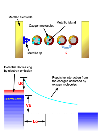
The model we consider in this work is briefly shown in Fig. 1. The internal structure of the device is that, between the two electrodes, there are some isolated metallic islands surrounded by oxygen molecules. The islands are formed during the deposition of top electrode, and the oxygen molecules are present when we do the measurement of pressure dependence, as will be discussed below. Because the islands are separated with electrodes, the electrons injected from the electrode to the islands must first tunnel the potential barrier formed by injection barrier of normal organic molecules, which is around 1eV depending on the LUMO or HOMO of organics and Fermi level of metals. The oxygen molecules adsorbed by the metallic islands in the organic film will act as deep traps to capture electrons, such that the barrier should be largely increased due to the repulsion between the conducting electrons and trapped electrons.Temperature Here, for simplicity, we have assumed that the distribution of adsorbed oxygen is an exponential decay from the top electrode with the decay length , and the density of trapped electron is linear in space. The transfer integral between neighboring islands is dependent on the distance between these islands. Within this structure, the metallic islands could form some conducting channels for electrons, so that electrons could transport from one electrode to the other via quantum tunnelings. The trapped electron in adsorbed oxygen molecules will influence the potential profile of the islands, and when the bias voltage is strengthened, the effect of NDR should be found.Datta On the other hand, when the device is switched to ON state, some metallic tips at metal-organic interface will form as discussed above, and then the injection barrier should be decreased due to the electron emission. In this sense, the current becomes larger and bistable effect emerges.
Based on the above description, we write down the model Hamiltonian of the system as
| (1) |
The first term for the electrode is
| (2) |
where is for left/right electrode, () the electron creation (annihilation) operator of the k-th continuum state in the electrode, the corresponding potential energy of that state, the bias voltage, and taking for left and for right. The second term of (1) for the metallic islands is
| (3) |
where () creates (annihilates) an electron at i-th metallic island, , the transfer integral between islands, and the charges adsorbed by oxygen molecules, which plays the essential role in this work. Wherein, the number of oxygen molecule adhering to the metallic islands, the filling factor, which will be assumed to be linear to . The interfacial injection potential induced by oxygen molecule is , and the length of the system is , which is not crucial when it is changed and will be set to throughout this work. In all, there are three adjustable parameters in this theory: is the interfacial injection potential, which determines the transition between OFF and ON state; is the coupling between neighboring islands, which is determined by how many islands are formed in the film, and we have neglected the disorder of ; is the penetration length of oxygen molecule, which is determined by the concentration of oxygens and the trapped electrons in them as well. All these parameters could be directly determined by the experiments, as is shown later.
The last term of (1) is the coupling between electrodes and islands, which has the form
| (4) |
where is the transfer integral between electrode and island. This parameter is directly related to the spectral broadening induced by electrodes, such that one can use it as a scaling to all results and then compare them with the experimental measurements.
Under a given bias voltage, a nonequilibrium steady state (NESS) could be achieved, and one can then calculate the corresponding I-V curve. To evaluate the tunneling current of NESS, we utilize the scattering operator method, which has been well developed by J. E. Han for the system of quantum dots.Han The basic idea of the method is to derive the scattering operators from the Lippmann-Schwinger equation and then evaluate the corresponding tunneling current.Han ; Hershfield Basically, the method we use in this work is straightforward from Han’s treatment, such that we would not go further to discuss the details of the method.
Based on the our model (1), we first try to rebuild the basic experimental I-V curves of both ON and OFF states for different device structures. The details of experiments are as follows. All the materials used were commercially available without any further purification. The devices were fabricated on ITO-coated glass substrates with sheet resistance about /sq. Each substrate was heated to C in air after solvent cleaning and then loaded into a high vacuum chamber (Pa). All the metallic and organic layers were formed by vacuum depositions. The deposition rate of Alq3, Mg and Al was about /s, /s and /s respectively. The area of the organic memory device was 9mm2, defined by 3-mm-wide ITO stripes overcrossed by 3-mm-wide top metal stripes. The current-voltage (I-V) characteristics of the devices were measured by a Keithley 236 unit with the top electrode grounded. The measurements of electric properties of the devices were carried out in a glove box (O1ppm and H2O1ppm) or a dewar (Janis Research Co. Inc. VTF-100) under 10-1Pa pumped by a mechanical pump.
In the left panels of Fig. 2, we show experimental measurements for three different structures by changing metallic electrodes. One can find some typical characteristics for these curves. For example, as the character of the memory effect, the OFF state current has a turn-on point at around V depending on the specific structure, while the ON state current goes up very quickly from 0V. Both ON and OFF state current have the similar line shape, that is, a wavepacket-like shape in a certain region of voltage. Especially, the downward sides of both states, say the NDR region, overlap heavily. The ratio between ON and OFF state and also the absolute value of them depend on the specific structure. In the right panels of Fig. 2, we show the corresponding theoretical results. It is shown that, all the results are in good agreement with the experiments. By changing , we have obtained the typical ON and OFF state current, respectively. That means, the memory effect is shown to correspond to the interfacial potential reduction, which is consistent with our previous experimental results. You2 On the other hand, the NDR effect has also been rebuilt by the theory, which is of importance in this type of memory device as we have mentioned.
To explain the NDR effect we found, we summarize the whole physical process inside our theory as follows: Initially, when the scanning bias voltage starts from zero, all the energy potentials on each metallic island are the same, and no current is present. Then the voltage increases gradually, and the current follows to increase instantaneously. At this moment, the potential on each island shifts and starts to differ from each other. As we know, the largest tunneling current emerges once the potential of each island coincides. That means, under a certain voltage, depending on the potential drop among the islands, the current will meet the maximum value and then go down, so that NDR effect occurs.
It is worth noting that, for each curve of the theoretical results, the change is about V from OFF to ON. Thus, if the metallic tip formed at the interface is estimated to be nm, the electric field it induces will be V/cm, much smaller than the estimation from experimenters.Yang1 The condition for the bistable effect becomes much softer in our theory. Meanwhile, the value of for each device at OFF state is comparable to the injection barrier of electron, which is consistent with the fact that the metallic islands, as donors, matter in the whole process.

To verify the present theory, we have to test it for independent experiments. Here, we show the results for different oxygen pressures, in Fig. 3. The left panels are for the ON state current of different structures under various pressures. It shows that, with increasing pressure, the current reduces very quickly. As the OFF state current is also much smaller than the ON state, this reduction of current is quite different from ON-OFF transition. The reason is that, compared with Fig. 2, there’s no turn-on point as the OFF state current shows, and also the downward sides separate largely. This indicates the oxygen plays a different role with the interfacial metallic tip, which matters in the ON-OFF transition. Another important point is that, we have also found (not shown here) the reduction of current is reversible, namely, when the pressure of oxygen is reset to a small value, the ON state current revives. More details of the experiment will be reported elsewhere. From this experiment, we can see that, the present of oxygen environment suppresses the memory effect heavily, which implies the essential role of oxygen in this type of memory devices.
In a common sense, the oxygen penetrates into the organic layer through the top electrode, due to the loose structure of organic materials. Hence, the penetration length is intuitively proportional to the pressure of oxygen. To study this effect more comprehensively, we could then change the to check if the theoretical result behaves the same as experiment. As the right panels of Fig. 3 show, we have rebuilt the experimental data, except within the high bias voltage region, in which the IV curves of devices undergo a shift due to some unknown cause. Typically, both the turn-on point and the downward side of the curves are the same with those from experiment. The explanation of this finding is as follows. When we change , it means the potential drop among the islands becomes quicker, such that the maximum value shifts to higher bias voltage. However, when we change , it means the potential drop in the film becomes slower, but the injection at the bottom electrode becomes harder. Within this understanding, the maximum point does not change very much, but the whole current curve goes down. This description could also explain why in those materials with good conducting performance, such as pentacene and CuPc, the memory effect is less robust.You1 That is, in these materials, the density of electron trapped by oxygen is larger than normal cases.

Finally, we would like to discuss the other type of organic memory device, say for example, that based on the electrochemical reaction.Island It was proposed that, a creation-and-rupture process of redox-controlled metallic bridges is respondence to the memory effect. Although this electrochemical process is quite different from the formation of metallic tips, to simulate it one can still act to change the interfacial potential as we do in this work. It implies that, the microscopic origin for different types of organic memory devices might be different, but the underlying mechanisms are intrinsically the same.
In summary, we have presented a theoretical model combining the effect of tunneling among metallic islands and interfacial electron emission due to the interfacial metallic tips to comprehensively investigate the underlying mechanism of organic memory devices. We calculate several sets of theoretical results, which compare well with corresponding experimental measurements in different devices. Based upon this comparison between theory and experiment, we conclude that the two essential effects in these devices, say memory effect and negative differential resistance, originate from the formation of metallic tips at interface and tunneling among metallic islands in the bulk, respectively. To further prove this conclusion, we show both theoretical and experimental results on the influence of oxygen, which shows a clear oxygen pressure dependence. Finally, we give an expectation on the influence by changing the thickness of organic film.
The authors would like to acknowledge the financial support from the National Natural Science Foundation of China and the National Basic Research Program of China (2012CB921401 and 2009CB929204).
References
- (1) B. Cho , S. Song , Y. Ji , T. W. Kim , and T. Lee, Adv. Funct. Mat. 21, 2806 (2011).
- (2) L. D. Bozano, B. W. Kean, V. R. Deline, J. R. Salem, and J. C. Scotta, Appl. Phys. Lett. 84, 607 (2004).
- (3) W. Tang, H. Shi, G. Xu, B. S. Ong, Z. D. Popovic, J. Deng, J. Zhao, and G. Rao, Adv. Mater. 17, 2307 (2005).
- (4) J. G. Simmons and R. R. Verderber, Proc. R. Soc. London, Ser. A 301, 77 (1967).
- (5) D. T. Simon, M. S. Griffo, R. A. DiPietro, S. A. Swanson, and S. A. Cartera, Appl. Phys. Lett. 89, 133510 (2006).
- (6) J. C. Scott and L. D. Bozano, Adv. Mater. 19, 1452 (2007).
- (7) R. Waser and M. Aono, Nature Mater. 6, 833 (2007).
- (8) R. E. Thurstans and D. P. Oxley, J. Phys. D 35, 802 (2002).
- (9) W. L. Kwan, B. Lei, Y. Shao, and Y. Yang. Current Applied Physics 10, e50 (2010).
- (10) M. Cölle, M. Büchel, D. M. de Leeuw, Org. Electron. 7, 305 (2006).
- (11) M. L. Wang, J. Zhou, X. D. Gao, B. F. Ding, Z. Shi, X. Y. Sun, X. M. Ding, and X. Y. Hou, Appl. Phys. Lett. 91, 143511 (2007).
- (12) Y. T. You, M. L. Wang, H. N. Xuxie, B. Wu, Z. Y. Sun, and X. Y. Hou, Appl. Phys. Lett. 97, 233301 (2010).
- (13) Y. T. You, Q. Zeng, Y. Yao, M. L. Wang, B. Wu, Y. He, Y. M. Hu, C. Q. Wu, and X. Y. Hou, Appl. Phys. Lett. 100, 123304 (2012).
- (14) M. L. Wang, X. Y. Sun, X. Y. Zheng, N. Li, X. D. Gao, B. F. Ding, X. M. Ding, and X. Y. Hou, Org. Electron. 10, 965 (2009).
- (15) B. Cho, J. M. Yun, S. Song, Y. Ji, D. Y. Kim, and T. Lee, Adv. Funct. Mat. 21, 3976 (2011).
- (16) B. Lei, W. L. Kwan, Y. Shao, and Y. Yang, Org. Electron. 10, 1048 (2009).
- (17) J. E. Han, Phys. Rev. B 73, 125319 (2006).
- (18) S. Datta, Quantum transport: atom to transistor, (Cambridge University Press, 2005).
- (19) S. Hershfield, Phys. Rev. Lett. 70, 2134 (1993).