Reply to Comment by Calandra et al on “Electronic Structure of Superconducting KC8 and Nonsuperconducting LiC6 Graphite Intercalation Compounds: Evidence for a Graphene-Sheet-Driven Superconducting State”
In their comment Calandra et al Calandra et al. , assert two points: (1) the estimate of charge transfer from Li to graphene layers in LiC6 in our letter Pan et al. (2011) is incorrect because of the three dimensional (3D) character of the electronic structure in bulk LiC6; (2) our main claim that the superconductivity in graphite intercalation compounds (GICs) is graphene-sheet-driven is therefore invalid.
First, we point out that our claim on graphene driven superconductivity in GICs is based on the experimental results from a whole series of different materials (graphite, KC, LiC6, KC8 and CaC6) and that it is valid regardless of the charge transfer estimate. In these different GICs, we observe a strong electron phonon coupling (EPC) between the graphene derived electrons and graphene derived phonons Valla et al. (2009); Pan et al. (2011). When put in the McMillan’s formula, the measured coupling constants give the superconducting transition temperatures, Tc, that are very close to the measured ones in LiC6, KC8 and CaC6, demonstrating that the graphene sheets are indeed crucial for superconductivity in GICs. The side observation that the filling of the states follows the same trend is in accord with a simple picture where the EPC strengthens as the phase space for the scattering grows with the size of the Fermi surface. However, this observation is not essential for the main conclusion of our letter. Second, we note that the validity of the calculations and the estimate for the charge transfer in Calandra et al is heavily based on comparison with the data from another material, lithium intercalated graphene bi-layer Sugawara et al. (2011), irrelevant for the studies of bulk GICs.
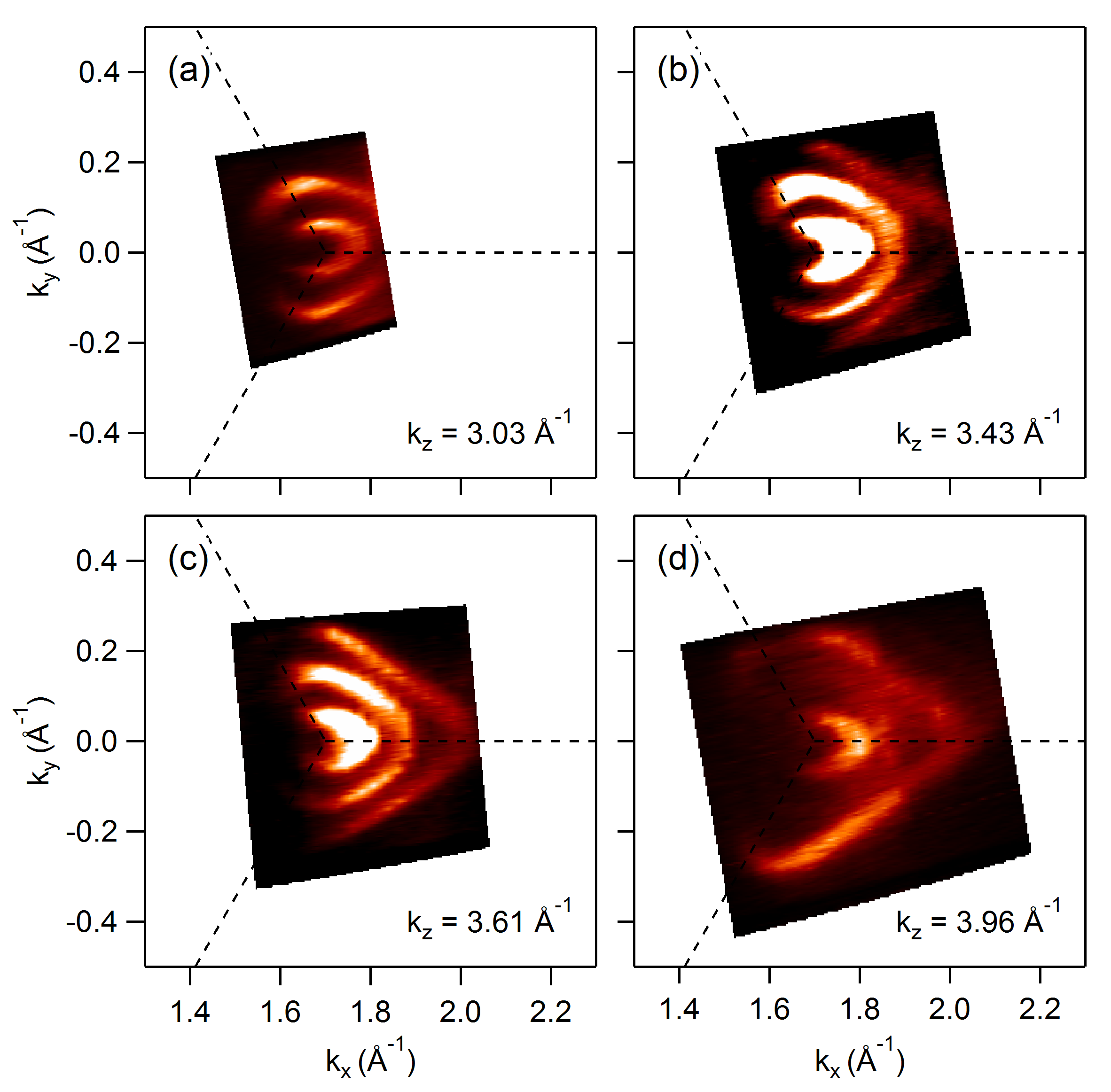
The third and the most important point is that the calculations for LiC6 show essentially a 3D electronic structure, virtually unchanged from the early work by Holzwarth et al Holzwarth and Rabii (1977), whereas our photoemission experiments show no out-of -plane dispersion. Fig. 1 shows the -derived Fermi surface (FS) of LiC6 recorded at different photon energies from samples with larger crystallites and a higher degree of intercalant order than those from Pan et al Pan et al. (2011). The three contours, originating from the AAA stacking in LiC6 below 220 K Kambe et al. (1979), are now clearly visible, indicating perfect stacking. The relative intensity of these three contours varies, but their areas do not change with . As the FS contours are sharper than in ref. Pan et al. (2011), the charge transfer could be more precisely determined: the FS area is somewhat larger than in ref. Pan et al. (2011), corresponding to the charge transfer of 0.052 e- per graphene unit cell (GUC), still significantly smaller than in KC8 (0.11 e-/GUC). The momentum averaged EPC is the same, within the error bars, to the value reported in Pan et al Pan et al. (2011). The lack of dispersion in the experiments clearly demonstrates inability of DFT calculations to correctly describe LiC6. A possible reason might be the wrong crystal structure - A, instead of the correct AAA stacking has always been used as a starting point in these calculations. However, for the problem of superconductivity in GICs, the more consequential issue is inability of the existing DFT calculations to account for the enhancement of the EPC on the -derived Fermi surface in GICs with doping, observed in many experiments, including ours Valla et al. (2009); Pan et al. (2011).

Z.-H. Pan1, A. V. Fedorov2, C. A. Howard3, M. Ellerby3 and T. Valla1
1Condensed Matter Physics and Materials Science Department, Brookhaven National Lab, Upton, NY 11973
2Advanced Light Source, Lawrence Berkeley National Laboratory, Berkeley, CA 94720
3London Centre for Nanotechnology and Department of Physics and Astronomy, University College London, London WC1E 6BT, United Kingdom
References
- (1) M. Calandra, C. Attaccalite, G. Profeta, and F. Mauri, Phys. Rev. Lett. (unpublished).
- Pan et al. (2011) Z.-H. Pan, J. Camacho, M. Upton, A. Fedorov, C. Howard, M. Ellerby, and T. Valla, Phys. Rev. Lett. 106 (2011).
- Valla et al. (2009) T. Valla, J. Camacho, Z.-H. Pan, A. Fedorov, A. Walters, C. Howard, and M. Ellerby, Phys. Rev. Lett. 102 (2009).
- Sugawara et al. (2011) K. Sugawara, K. Kanetani, T. Sato, and T. Takahashi, AIP Advances 1, 022103 (2011).
- Holzwarth and Rabii (1977) N. Holzwarth and S. Rabii, Mater. Sci. Eng. 31, 195 (1977).
- Kambe et al. (1979) N. Kambe, M. Dresselhaus, G. Dresselhaus, S. Basu, A. McGhie, and J. Fischer, Mater. Sci. Eng. 40, 1 (1979).