Graphene nanoring as a tunable source of polarized electrons
Abstract
We propose a novel spin filter based on a graphene nanoring fabricated above a ferromagnetic strip. The exchange interaction between the magnetic moments of the ions in the ferromagnet and the electron spin splits the electronic states, and gives rise to spin polarization of the conductance and the total electric current. We demonstrate that both the current and its polarization can be controlled by a side-gate voltage. This opens the possibility to use the proposed device as a tunable source of polarized electrons.
pacs:
72.80.Vp; 73.22.Dj; 73.22.-f1 Introduction
Graphene is a material with a combination of many remarkable properties, in particular, large electron mobility and long spin-coherence lengths up to several microns [1, 2, 3]. These features spurred the interest in graphene as a material of choice for spintronic devices which exploit both the charge and the spin degrees of freedom as the basis of their operation. Geim and coworkers used soft magnetic NiFe electrodes to inject polarized electrons into graphene and found spin valve effects [4]. Later, Cho et al. performed four-probe spin-valve experiments on graphene contacted by ferromagnetic Permalloy electrodes [5], observing a switching of the sign in the four-probe nonlocal resistance, which indicates the presence of a spin current between injector and detector. The drift of electron spins under an applied dc electric field in spin valves in a field-effect transport geometry at room temperature was studied in Ref. [6]. These experiments were found to be in quantitative agreement with a drift-diffusion model of spin transport. More recently, Dedkov et al. proposed that the Fe3O4 /graphene/Ni trilayer can also be used as a spin-filtering device, where the half-metallic magnetite film was used as a detector of spin-polarized electrons [7].
With the development of the nanoscale technology of graphene, a number of nanodevices have been proposed to explore novel spin-dependent transport phenomena. Spin filter effects in graphene nanoribbons with zig-zag edges were investigated theoretically by Niu and Xing using a non-equilibrium Green function method [8]. They found a fully polarized spin current through ferromagnetic graphene/normal graphene junctions, whose spin polarization could be manipulated by adjusting the chemical potential of the leads. Ezawa investigated similar effects in a system made of graphene nanodisks and leads, where the magnetic moment of the nanodisk can be controlled by the spin current [9]. Guimarães et al. studied spin diffusion in metallic graphene nanoribbons with a strip of magnetic atoms substituting carbon ones in the honeycomb lattice [10]. They found that the system behaves as a spin-pumping transistor without net charge current. More recently, Zhai and Yang have shown that the combined effects of strained and ferromagnetic graphene junctions can be used to fabricate a strain-tunable spin filter [11]. All these findings open the possibility of designing spintronic devices based on graphene nanostructures for memory storage and spin diodes. For a more complete and detailed review on the electronic and spin properties of mesoscopic graphene structures and control of the spin see, for example, Ref. [12] and references therein.
Recently we have proposed a novel design of a quantum interference device based on a graphene nanoring, in which all edges are of the same type to reduce scattering at the bends [13]. Electron transport in the device can be controlled by a gate voltage applied across the nanoring between two side electrodes. The relative phase of the electron wave function in the two arms of the ring can be varied by the side-gate voltage, leading to constructive or destructive interference at the drain, which results in conductance oscillations and electric current modulation. In this paper we show that such controlled interference can also be used to design an efficient spin filter device. The latter can be achieved by depositing a ferromagnetic insulator below (or above) the nanoring, in which case the combination of the exchange splitting due to the interaction of the electron spin with the magnetic ions and the effect of the side-gate voltage can result in a controllable spin-polarized electric current.
2 Graphene nanoring: Model and formalism
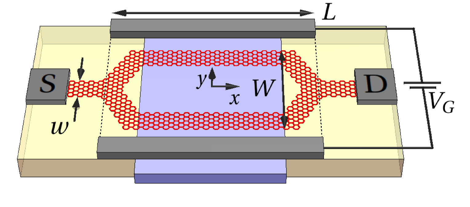
The quantum interference device introduced in Ref. [13] consists of a graphene nanoring with bends attached to two graphene nanoribbons which, in turn, are connected to source and drain terminals, as shown in figure 1. The width of all nanoribbons is . Two lateral electrodes allow to apply a side-gate voltage. The total length of the ring is while the total width is . Note that these dimensions should be large enough to avoid dielectric breakdown at used source-drain and side-gate voltages.
The dispersion relation of graphene nanoribbons is known to be very different from that of the bulk graphene [14]. In particular, their band structure has a width-dependent gap that turns out to be very sensitive to the type of the nanoribbon edge (zig-zag or armchair) [15]. In the most general case, the edge type changes at a nanoribbon bend, which results in the energy levels mismatch and can decrease the transmission and the current considerably. To reduce the back scattering at bends, we proposed to use bends in order to keep all edges of the device of the same type [13]. Recent studies indicate that atomic-scale precision along the edges can be achieved experimentally [16], promising a possibility to fabricate the proposed device. Hereafter we restrict ourselves to nanoribbons with armchair edges, for which the energy spectrum is centered around . This type of nanoribbon was found to be the most advantageous one for electronic transport because the transmission spectrum of such a system presents wide bands of high transmission probability [13].
The applied side-gate voltage results in different energy shifts of the electronic states in the two arms of the ring. Thus, a charge carrier injected from the source nanoribbon couples to different modes of the two arms. These two modes can interfere constructively or destructively at the drain, giving rise to conductance and current modulation depending on the side-gate voltage [13]. We note that this form of current control relies on interference effects which depend quantitatively on details of device geometry, material parameters, perturbations, such as the disorder, etc. However, the underlying principle of operation is very basic and as long as there exist propagating modes in the two arms of the ring, the control is expected to be feasible. We will use therefore simple models which grasp the main features of the different system components.
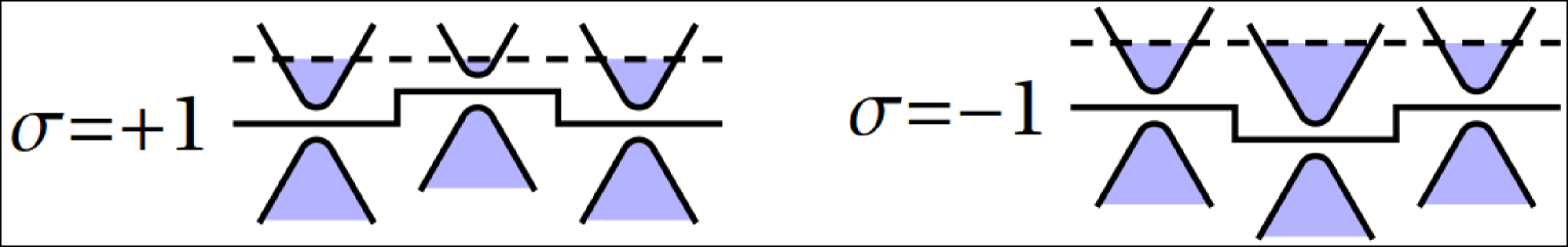
In the present design we consider a nanoring fabricated above a strip of a ferromagnetic insulator, such as EuO. The exchange interaction between Eu2+ ions and charge carriers can be described as an effective Zeeman splitting of the spin sublevels [17]. This creates spin-dependent potential profiles along the arms of the ring (see figure 2), so an injected electron couples to different modes of the arms depending on its spin and therefore, for some side-gate voltages, the interference governing the conductance can be constructive for spin-up and destructive for spin-down states (or vice versa), resulting in a spin polarized total current.
To model the device we have considered a simple tight-binding Hamiltonian of a single electron in the orbitals of graphene within the nearest-neighbor approximation
| (1) |
where the site energy depends on the position of the -th carbon atom, in particular, due to the side-gate voltage. Following Ref. [13] we use a simplified side-gate potential profile: if the origin of the coordinate system is in the geometrical center of the ring (as indicated in figure 1), this potential is linear in the direction for while in the direction it is (i) constant within the nanoring area () and (ii) decays exponentially towards the two leads (for ). The contacts are assumed to be far enough from the ring, so that the side-gate potential can be safely set to zero at the leads. The total potential drop between the outer edges of the two arms (separated by the distance ) is denoted as and is referred to as the side-gate voltage from now on.
The ferromagnet also affects the site energies , shifting them by the amount , where is the exchange splitting amplitude and () for spin up (spin down) states. Throughout the paper we use the value of meV, which is of the order of the values known from the literature [17, 18, 19]. Because the characteristic length scale of the exchange interaction is of the order of one monolayer thickness, [17] we assume that only the sites which are in touch with the ferromagnetic strip are affected by the interaction; the set of such sites belonging to the longitudinal sections of the arms (see figure 1) is denoted as in equation (1). Due to such local splitting, a spin up (down) electron propagating along one of the arms is subjected to the potential with a rectangular barrier (well). Such potential profile is shown schematically in figure 2 for the case of zero side-gate voltage.
The graphene lattice is known to undergo reconstruction at nanoribbon edges, which affects the corresponding site energies and hoppings [15]. These effects are not expected to play a crucial role for transport properties of realistic disordered samples (see Ref. [13] for details), and therefore we neglect them and consider an undistorted honeycomb lattice with nearest neighbor coupling eV [20].
The quantum transmission boundary method [21, 22] combined with the effective transfer matrix approach [23] were used to calculate wave functions and spin-dependent transmission coefficients for spin up () and spin down () electrons. These coefficients depend on the energy of the injected carrier and the side-gate voltage and allow to obtain the degree of transmission polarization
| (2) |
as well as spin polarized currents . To calculate the latter we used the Landauer-Büttiker scattering formalism
| (3) |
where is the Fermi-Dirac distribution, being the Boltzmann constant. Here we assume that the source-drain voltage drops in the leads, which agrees with recent experimental results [24], and model the effect of this voltage drop as a shift of the Fermi level of the source, , with respect to that of the drain, . Then, one can calculate the total current through the device
| (4) |
and its polarization
| (5) |
Finally, we note that equation (3) is valid in the one-mode approximation [25]. Hereafter, we assume that our system is operating in the one-mode regime, which implies that the lateral quantization energy (due to the finite nanoribbon width ) is much larger than the source-drain voltage and the temperature . Further requirements for the latter two parameters are discussed below.
3 Results and discussion
The sample that we consider is a nanoring made of nanoribbons of width nm with armchair edges. The full length of the ring is nm while the full width is nm (see figure 1 for the schematics of the device).
First, we address the device properties at zero side-gate voltage. Transmission coefficients as functions of the carrier energy are shown in the upper panel of figure 3. If the substrate is not ferromagnetic there is no exchange splitting () and the spin does not play any role, so are degenerate (see the black curve in the figure). In this reference case the transmission is characterized by a series of peaks or bands which become wider as the carrier energy increases. The interaction with the ferromagnet shifts these features towards lower or upper energies depending on the sign of the carrier spin (see the red dotted curve giving and the blue dashed one giving ). Note that the transmission spectrum remains qualitatively the same except for the energy shift. Peak shifts are shown using arrows above the curves in the upper panel.
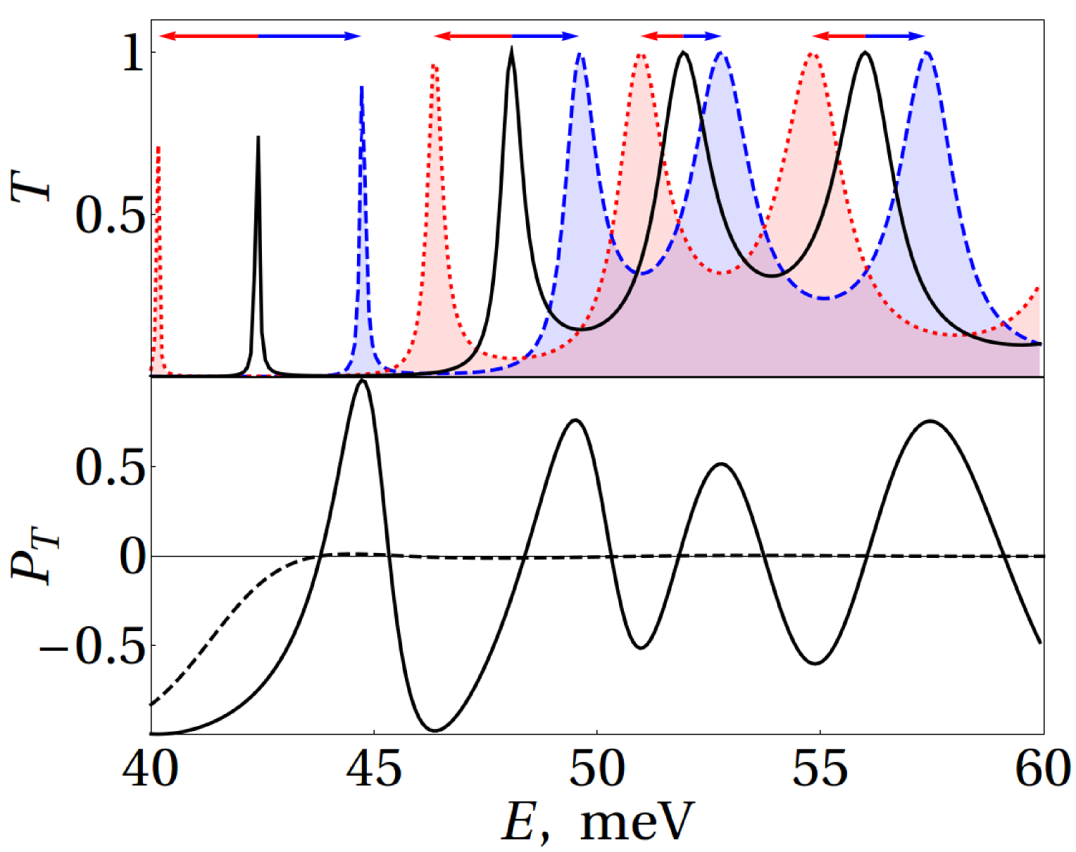
Lower panel of figure 3 shows the degree of the transmission polarization, as defined by equation (2), demonstrating that the transmission is highly polarized within some energy ranges. The latter can give rise to the spin polarized electric current. The polarization degree is higher at lower energies. However, the transmission coefficient in this energy range comprises narrow resonance peaks which can easily be destroyed by perturbations such as disorder, as we show below. The higher energy range with its wider transmission bands, being more robust under the effects of disorder [13], is more promising for applications. For comparison, we also calculated the transmission polarization for a single nanoribbon of the same width and length as those of the quantum ring (see the dashed line in the lower panel of the figure). As expected, the interference effects are absent and the transmission polarization disappears quickly as the carrier energy increases.
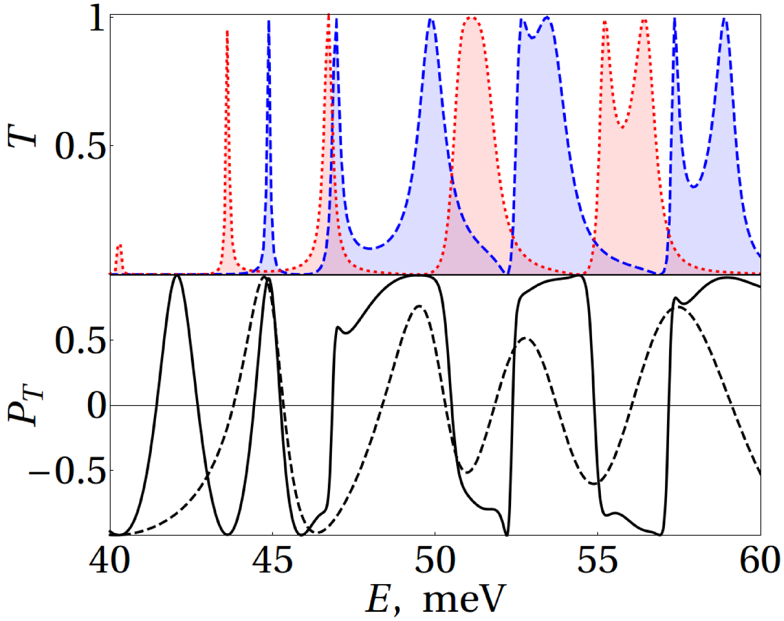
Next, we study the effect of the side gate voltage on the polarization of the electric current. To this end, we calculated the transmission coefficient maps for spin up and spin down electrons. These results are shown in the upper and middle panels of figure 4. Using them, we obtained the transmission polarization degree presented in the lower panel of the figure, which demonstrates that the polarization can be controlled by the side-gate voltage. Hereafter, we focus on the higher energy range ( meV in the considered case) where wider transmission bands have the interference nature [13]. As can be seen from the figure, the sign of the polarization is almost independent of the side-gate voltage for some energies (see the leftmost and the middle shadowed strips), while for others both the polarization degree and its sign can be changed by the side-gate (see, e. g., the rightmost shadowed strip), which opens the possibility to control the polarization of the current by the electrostatic gate.

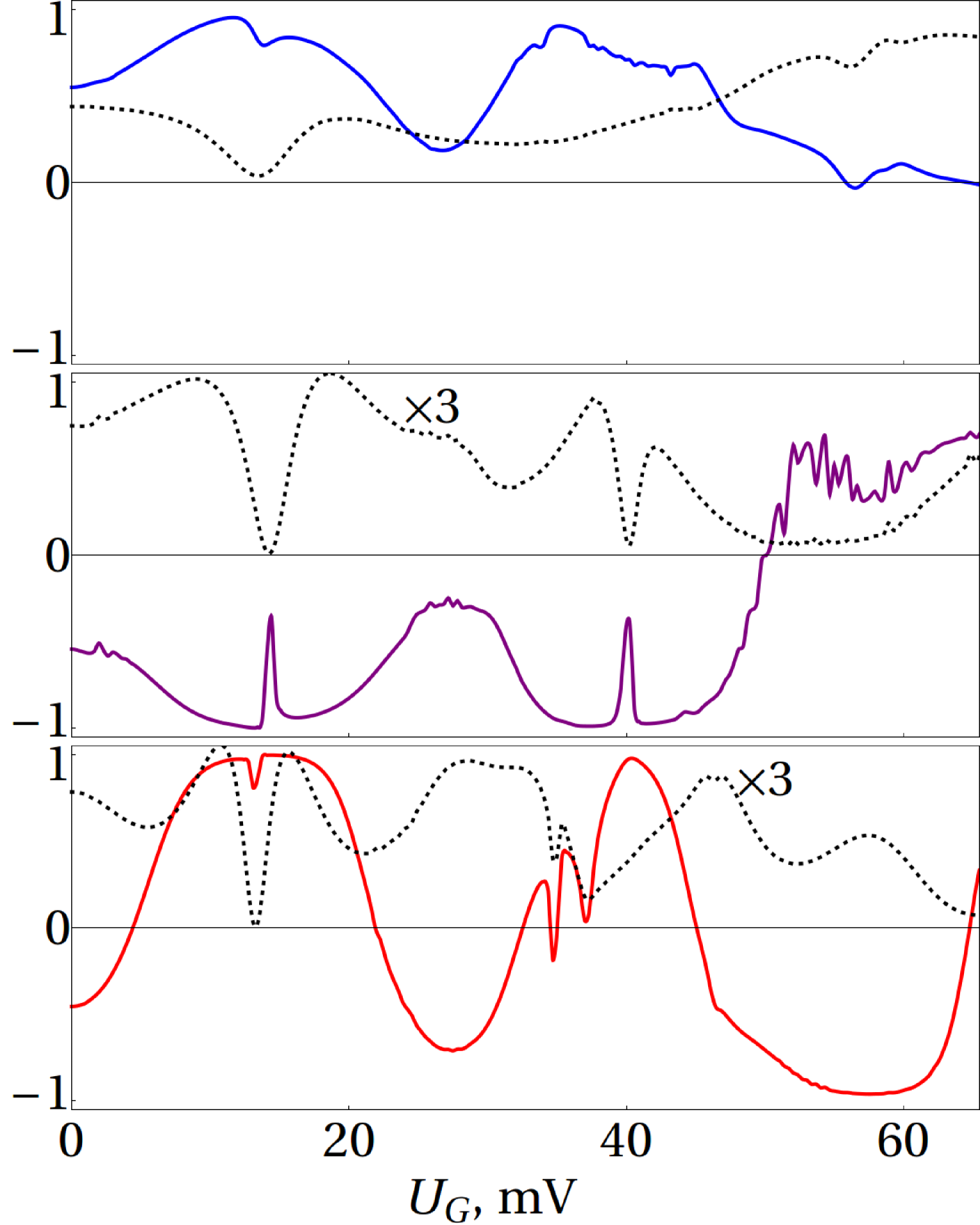
To demonstrate this possibility, we calculated the total current together with its polarization degree according to equations (4) and (5). We assume that Fermi energies of both the source and the drain are set to some value by a back-gate voltage and then one of these levels is shifted with respect to the other by the source-drain voltage . Upper and lower limits of the three shadowed strips in figure 4 give the source and drain Fermi energies and , respectively, which were used to calculate electric currents from equation (3) for mV and K. This choice of values was suggested by the following reasoning. At the Fermi distributions are step functions, so only the energy range between and contribute to the current [see the integrand in equation (3)]. If this range is greater than the typical energy separation between the transmission bands of and (see figure 4), then both polarizations would contribute to the total current to a similar extent and its polarization would be reduced. Therefore, to observe substantial current polarization, should be smaller than the typical energy scale in the transmission maps. Figure 4 suggests that this scale is of the order of meV, which justifies our choice of mV. Similar arguments apply to the temperature which smears out the Fermi step functions, increasing the range of energies contributing to the current and reducing its polarization. Thus, the temperature should be smaller than K.
Figure 5 shows the total current (dotted lines) and its polarization degree (solid lines). Upper, middle and lower panels correspond to the leftmost, middle and rightmost shadowed strips in figure 4, respectively. As expected, the electric current can be highly polarized. For some combinations of the source and drain Fermi energies, the sign of the current polarization remains the same within wide ranges of the side-gate voltage (see the upper and the middle panels of figure 5). Nevertheless, as can be seen from the lower panel, the Fermi energies at the source and drain can be adjusted in such a way that the current polarization can be changed in almost its entire possible range by the side-gate voltage, suggesting that the proposed device operates as a controllable source of spin-polarized electrons.
We note that we have considered an ideal symmetric nanoring while different imperfections or perturbations, in particular, the disorder, can affect the electric current and its polarization. There are various possible sources of disorder, for example, charged impurities in the substrate or defects of the device fabrication, such as imperfections of the device edges. While the former would provide some additional smooth electrostatic potential and can hardly deteriorate the transmission through the device to a large extent, the impact of the latter on the transport properties is probably stronger, especially for small devices.
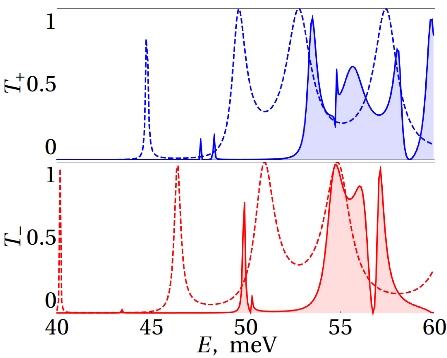
Following Ref. [13], in order to estimate a possible impact of the edge disorder on the transport properties, we consider a sample in which we remove pairs of carbon atoms from the nanoring edges with some given probability . Transmission coefficients calculated for one particular realization of such a disorder for and zero side-gate voltage are presented in the upper and lower panels of figure 6, respectively. Dashed lines show the transmission coefficients of the reference ordered sample while solid lines show those of a disordered one. In the disordered sample all transmission bands are shifted to higher energies with respect to their positions in the regular one because, by removing atoms from the edges, the ribbons are made effectively narrower. This leads to higher quantization energy in the lateral direction that manifests itself in the observed shifts. As expected, narrow resonance peaks in the lower energy range (meV) almost disappear in the disordered sample while wider interference-related bands at higher energies are not destroyed by the disorder. These bands are affected by the disorder to a comparable degree for both spin up and spin down electrons, which suggests that a moderate disorder would not deteriorate polarization properties of the spin filter to a large extent.
Finally, we address possible effects of a different kind of imperfections of the device fabrication on its performance. One of them is a change of the length of one of the arms at a fixed nanoribbon width . Such a change would affect the interference at the drain, and one can expect the transmission peaks appearing at different side-gate voltages, while the overall picture remaining qualitatively the same. We have checked the validity of this intuitive argumentation by numerical calculations (results are not presented here).
The fabrication imperfection that could have a more profound impact on transport is a change of the width of one of the arms. In this case, the lateral quantization in this wider (or narrower) part of the ring is different, resulting in a mode mismatch at the boundary, which can reduce the transmission. In order to estimate the corresponding effect, we added an extra layer of atoms to the horizontal part of the upper arm and calculated and . The results are presented in figure 7, where the upper panel shows the transmissions for the asymmetric sample at zero side-gate voltage, . Comparing the transmission coefficients in the upper panel of the figure with those in figure 3 one can see that, as can be expected, the asymmetry shifts the transmission peaks. Besides, the overlaps between the transmission bands are reduced in the case of the asymmetric nanoring. The bands are more isolated, which results in the most important effect: the polarization sign can be switched much more abruptly, making the asymmetric design more advantageous for applications.
To conclude the discussion of the impact of fabrication imperfections on the device properties, we note that, because the interference is very sensitive to many details, different samples could be expected to have quantitatively different current-voltage characteristics. However, as we have shown above, qualitatively the transmission coefficient and its polarization remains the same. It can then be expected that as long as the size of the ring, temperature, and applied voltages are such that the system remains within the one-mode regime, the device can operate as a tunable spin filter.
4 Summary
In summary, we have proposed and studied a novel spin filter which exploits quantum interference effects. The device comprises a graphene nanoring with 60∘ bends fabricated above a ferromagnetic strip. We showed that due to the exchange splitting induced by the magnetic ion of the ferromagnetic layer, the transmission coefficient is different for spin up and spin down electrons, giving rise to the polarization of the conductance and the electric current. We demonstrated that both the current and its polarization can be controlled by a side-gate voltage. Predicted effects are shown to be robust under a moderate edge disorder and other fabrication imperfections, such as the asymmetry of the ring. Therefore, we conclude that the proposed device is a promising candidate for real world applications, in particular, it can be used as a tunable source of polarized electrons.
Work at Madrid was supported by MICINN (Projects Mosaico and MAT2010-17180). P. A. O. acknowledges support from FODNECYT (Project 1100560).
References
- [1] Kane C L and Mele E J 2005 Phys. Rev. Lett. 95 226801
- [2] Tombros T, Jozsa C, Popinciuc M, Jonkman H T and van Wees B J 2007 Nature 448 571
- [3] Yazyev O V 2008 Nano Lett. 8 1011
- [4] Hill E W, Geim A K, Novoselov K, Schedin F and Blake P 2006 IEEE Trans. Magn. 42 2694
- [5] Sungjae Cho, Yung-Fu Chen and Fuhre M S 2007 Appl. Phys. Lett. 91 123105
- [6] Józsa C, Popinciuc M, Tombros N, Jonkman H T and van Wees B J 2008 Phys. Rev. Lett. 100 236603
- [7] Dedkov Yu S , Generalov A, Voloshina E N and Fonin M 2011 Phys. Stat. Sol. RRL 5 226
- [8] Niu Z P and Xing D Y 2010 Eur. Phys. J. B 73 139
- [9] Ezawa M 2009 Eur. Phys. J. B 67 543
- [10] Guimarães F S M, Costa A T, Muniz R B and Ferreira M S 2010 Phys. Rev. B 81 233402
- [11] Zhai F and Yang L 2011 Appl. Phys. Lett. 98 062101
- [12] Rozhkov A V, Giavaras G, Bliokh Y P, Freilikher V and Nori F 2011 Phys. Rep. 503 77
- [13] Munárriz J, Domínguez-Adame F and Malyshev A V 2011 Nanotech. 22 365201
- [14] Nakada K, Fujita M, Dresselhaus G and Dresselhaus M S 1996 Phys. Rev. B 54 17954
- [15] Son Y–W, Cohen M L and Louie S G 2006 Phys. Rev. Lett. 97 216803
- [16] Jia X, Hofmann M, Meunier V, Sumpter B G, Campos-Delgado J, Romo-Herrera J M, Son H, Hsieh Y–P, Reina A, Kong J, Terrones M and Dresselhaus M S 2009 Science 323 1701
- [17] Haugen H, Huertas-Hernando D and Brataas A 2008 Phys. Rev. B 77 115406
- [18] Zou J, Jin G and Ma Y–Q 2009 J. Phys.: Condens. Matter 21 126001
- [19] Gu Y, Yang Y H, Wang J and Chan K S 2009 J. Appl. Phys. 105 103711
- [20] Castro Neto A H, Guinea F, Peres N M R, Novoselov K S and Geim A K 2009 Rev. Mod. Phys. 81 109
- [21] Lent C S and Kirkner D J 1990 J. App. Phys. 67 6353
- [22] Ting D Z–Y, Yu E T and McGill T C 1992 Phys. Rev. B 45 3583
- [23] Schelter J, Bohr D and Trauzettel B 2010 Phys. Rev. B 81 195441
- [24] Venugopal A, Colombo L and Vogel E M 2010 Appl. Phys. Lett. 96 013512
- [25] Büttiker M, Imry Y, Landauer R and Pinhas S 1985 Phys. Rev. B 31 6207