Improving the Quality Factor of Microwave Compact Resonators by Optimizing their Geometrical Parameters
Abstract
Applications in quantum information processing and photon detectors are stimulating a race to produce the highest possible quality factor on-chip superconducting microwave resonators. We have tested the surface-dominated loss hypothesis by systematically studying the role of geometrical parameters on the internal quality factors of compact resonators patterned in Nb on sapphire. Their single-photon internal quality factors were found to increase with the distance between capacitor fingers, the width of the capacitor fingers, and the resonator impedance. Quality factors were improved from 210,000 to 500,000 at T = 200 mK. All of these results are consistent with our starting hypothesis.
Improving the internal quality factor of on-chip microwave superconducting resonators is a key development for quantum information processing and photon detectors Wang et al. (2011); Mazin et al. (2006). The internal quality factor at single-photon powers, , of particular interest for quantum information applications, is observed to be 10-100 times lower than high-power quality factors Lindstroem et al. (2009); Vissers et al. (2010); Barends et al. (2010); Khalil et al. (2011); Weber et al. (2011). Ideas for increasing resonator include switching from conventional metals like Nb or Al to alloys such as TiN or NbTiN Barends et al. (2008); Vissers et al. (2010); Leduc et al. (2010); Barends et al. (2010), using interface layers of SiN Vissers et al. (2010), etching the substrate between traces Barends et al. (2010), depositing metal under special conditions Megrant et al. (2012), or using low loss substrates Weber et al. (2011). Results from these experiments have generated the hypothesis that resonator is limited by a surface two level system (TLS) distribution Gao et al. (2008); Barends et al. (2008); Khalil et al. (2011); Barends et al. (2010).
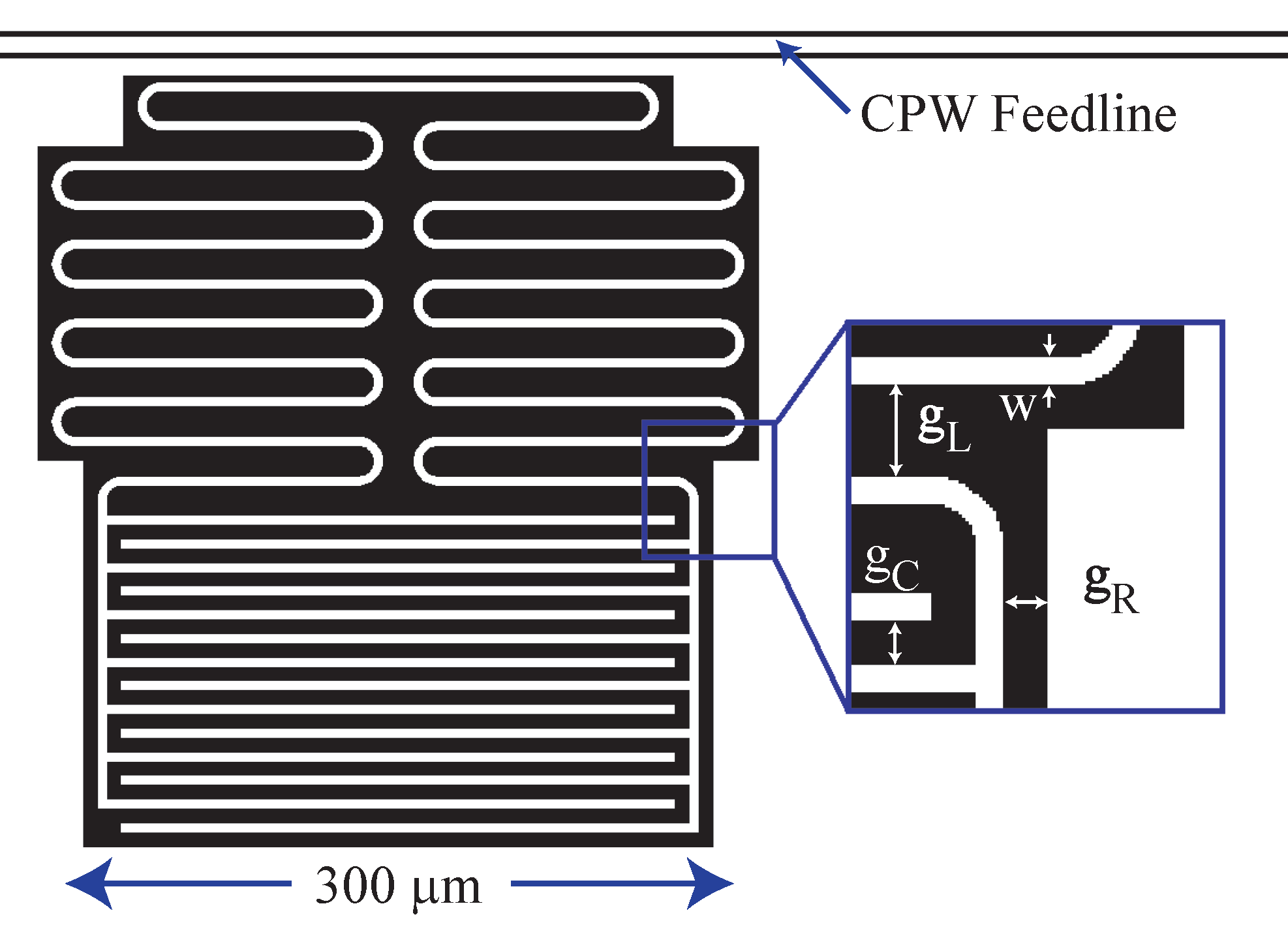
Motivated by a previous study that showed that the of coplanar waveguide (CPW) resonators increases with increasing gap Gao et al. (2008), we extended the idea of geometrical optimization to compact resonators Khalil et al. (2011); Lindstroem et al. (2009); Leduc et al. (2010). Compact resonators, as shown in Figure 1, consist of a meander inductor in parallel to an interdigitated capacitor. Their small size makes them an ideal element for multi-qubit processors. While compact resonators have been shown to have similar as the more widely used CPW resonators Khalil et al. (2011), they permit more design choices. Here we show that by changing parameters linked to the surface participation ratio, we have optimized these resonators to achieve an improvement by a factor of 2.4 0.2. We have thus been able to reach a of 500,000 at a resonator temperature of 200 mK, our point of reference. In this paper, we prefer to quote at this temperature because we believe that even when the sample box is anchored to a colder plate, resonator temperatures substantially below 200 mK may not be reached reliably. We return to this point later in the paper.
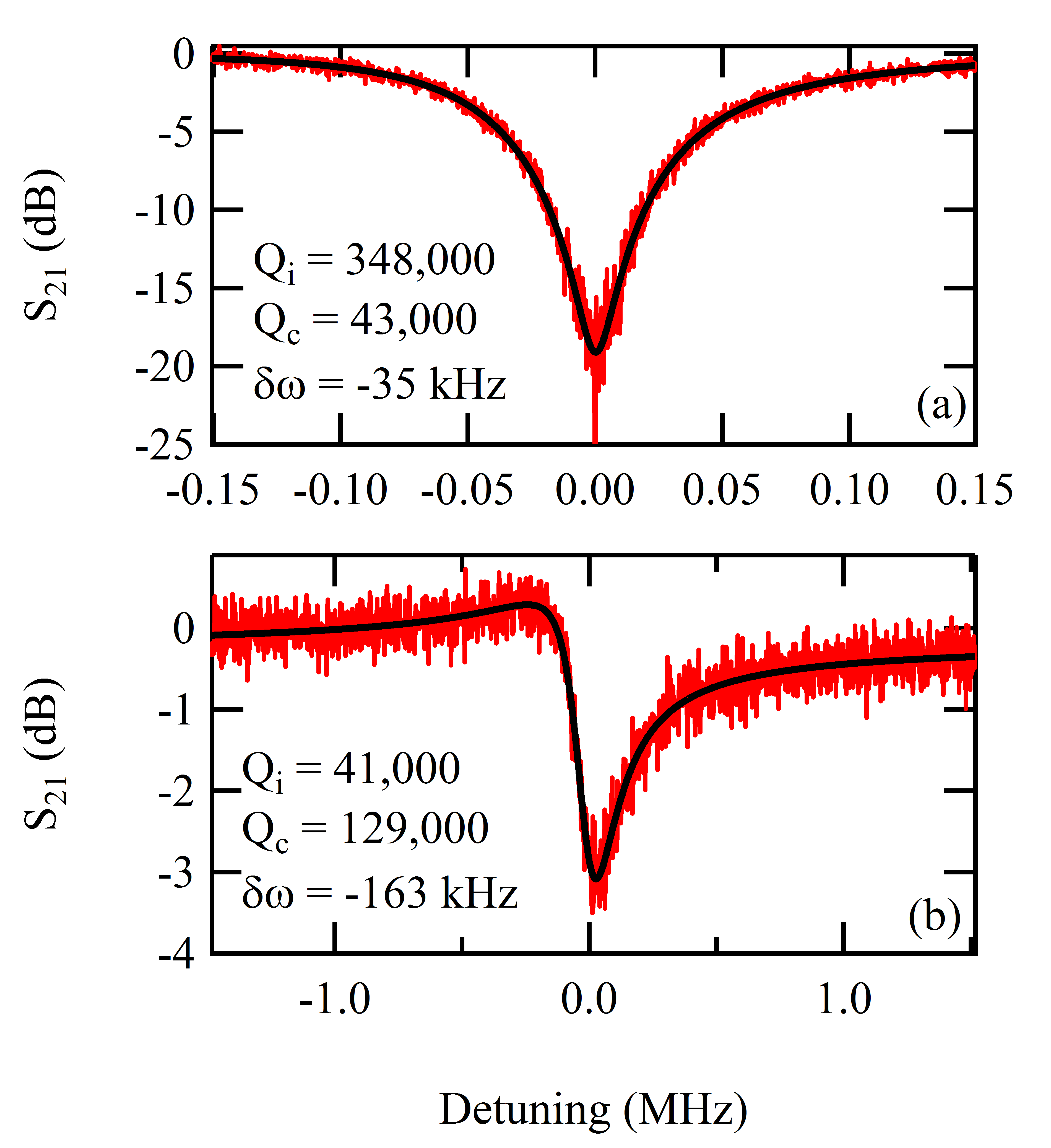
We measure the quality factor of our compact resonators by performing a microwave transmission experiment. Coupling to the resonators is achieved by placing the resonator in a cutout in the ground plane of a CPW feedline, relying on the mutual inductance between the feedline and the resonator inductor. This coupling introduces a second quality factor, the coupling quality factor . Typical values of that we designed ranged from 20,000 to 150,000. As a control experiment, we have designed and measured resonators with as high as with no change in . As shown in Megrant et al. (2012); Khalil et al. (2012), the measurement of microwave transmission through the feedline as a function of frequency provides access to . Although simple resonator models predict a symmetric response, the measured response is typically asymmetric due to reflections in the feedline circuit, as shown in Figure 2. Nevertheless, the theory of the arbitrary linear circuit model with one pole and perfect transmission at zero frequency shows that the asymmetric response can still be fit to separately extract and by introducing an extra parameter characterizing the asymmetry. We thus analyze our data with Equation 1, where the total quality factor, , is defined as .
| (1) |
This expression is exactly equivalent to Eq. (13) in Khalil et al. (2012) and to Eq. (3) in Megrant et al. (2012) with a different parametrization.
In our measurement setup, we cool 4 chips at once in a dilution refrigerator with a base temperature of 80 mK (sample temperature of approximately 200 mK). Since each of our chips contained one feedline coupled to 6 independent resonators at frequencies between 5 and 8 GHz, 24 resonators were tested in each cooldown. The chips were wire-bonded to a printed circuit board with Arlon dielectric and placed inside a copper sample box. The box was mounted inside a magnetic shield (Amuneal A4K) and attenuators were installed totaling 50 dB on the input microwave line. All four chips were excited simultaneously using a passive 4-way microwave splitter. The output line consisted of two Pamtech 4-8 GHz isolators on the mixing chamber, a 12 GHz low-pass filter on the 700 mK stage, and a Caltech HEMT amplifier at the 4 K stage. The measurement line was switched between the 4 chips using a microwave switch (Radiall R573423600) mounted on the mixing chamber.
Our resonators were fabricated using etched Nb on c-plane sapphire. Before metal deposition, the sapphire surface was prepared by a 60 s ion-milling using a 3 cm Kaufmann source that shoots 500 eV Argon ions at our wafer. Our source operates at a flow rate of 4.25 sccm and a pressure of about 10 Torr, generating a current density of 0.67 mA/cm2. A 200 nm layer of Nb was then dc magnetron sputtered on the wafer. Photolithography was performed by patterning directly onto S1808 resist using a 365 nm laser. After development, the Nb was etched using a 1:2 mixture of Ar: at 10 mTorr for 3 minutes. The wafer was then diced into individual chips for measurement.
In the systematic variation of compact resonator parameters, we chose to optimize the following parameters shown pictorially in Figure 1; the gap between two adjacent capacitor fingers, the distance between two adjacent inductor meanders, the distance between the resonator and the surrounding ground plane, and the width of the resonator traces. In addition, we also varied the characteristic impedance of the resonator. This set of parameters is relevant for surface losses.
We formed a benchmark set of resonators with parameter values: = 10 m, = 20 m, = 10 m, = 5 m and = 100 Ω. Resonators with this set of parameters will now be called “Design A” resonators. We measured 25 Design A resonators with an average of 160,000(20,000) and a maximum of 210,000 at single-photon power. Additionally, one chip with 6 resonators inexplicably had quality factors ranging from 40,000 to 70,000, much lower than the rest; we did not include this chip in the benchmark. typically increased to around at a “high” power corresponding to an average of photons in the resonator. The resonant frequency typically decreased as the temperature passed below 1.3 K, consistent with TLS loss Gao et al. (2008). These results are consistent with the hypothesis that our benchmark is controlled by surface losses.
We measured 24 geometrical variants of Design A, with each “mutant” resonator having only one parameter value that is changed. For example, the mutant values of were: 3, 5, 20, 30, and 40 m. The results of the mutant resonators are shown in Figure 3; percent changes in are given with respect to the Design A resonator benchmark.
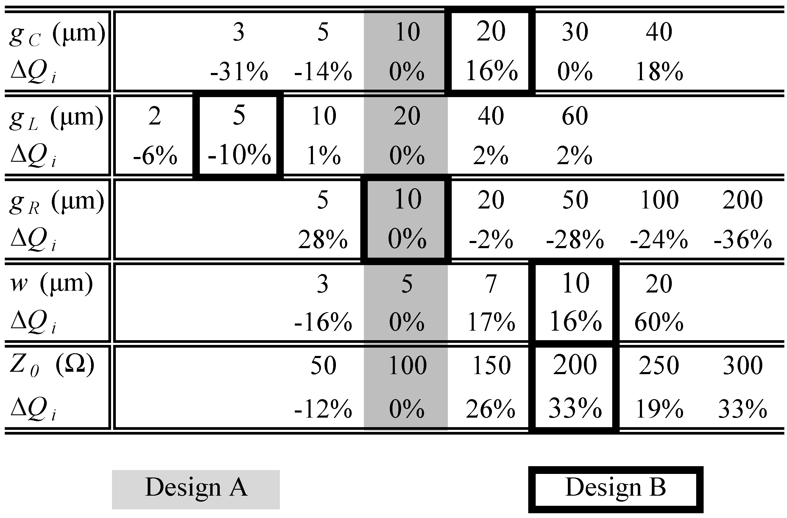
For , small values lead to lower , and larger values lead to higher . The effect of changing on is at least a factor of three smaller than for . Thus the gaps where electric fields are present (the capacitor and not the inductor), partially control , consistent with a surface loss mechanism coupled to the electric field. Similarly increases for larger , again consistent with surface loss since wider traces lead to decreasing electric field strength at surfaces. Next, we find that drops by roughly 25% if 50 m, suggesting that the ground plane prevents electric fields from reaching lossy materials such as the copper box or PCB dielectric. Lastly, the trend indicating that larger values of are beneficial to appears to contradict the usual hypothesis that dissipative mechanisms have a constant . The results for , and are all consistent with a loss dominated by surface electric field participation.
We chose two new sets of parameters from these results with the goal of improving the . Resonators with these parameters are called Design B and Design C resonators. Design B values were chosen to be relatively modest changes from Design A, while Design C values were chosen to maximize . Design B chosen values were: = 20 m, = 5 m, = 10 m, = 10 m and = 200 Ω. Resonator size increases rapidly with since the larger requires twice the inductance. Therefore, to limit the overall size to roughly 700 m x 500 m, we reduced to 5 m, despite the fact that this may lower by 10%. Design C chosen values were: = 80 m, = 10 m, = 10 m and = 300 Ω. Note that was chosen beyond the range of tested mutant Design A resonators. Also in Design C, the trace width was different for the capacitor (40 m) and inductor (10 m) halves in order to benefit from the larger capacitor width while keeping the resonator from being larger than 1000 m x 1000 m.
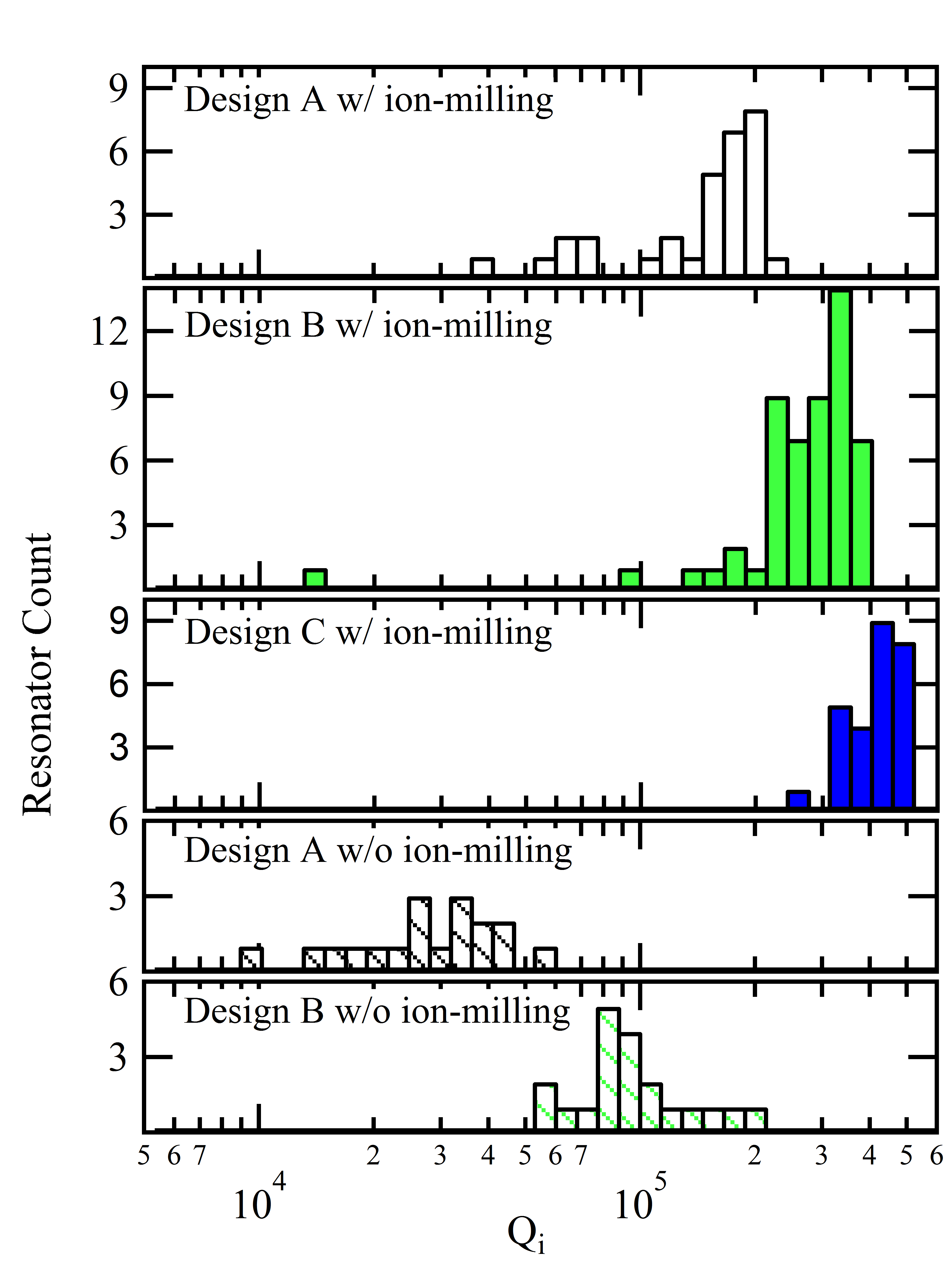
The results of all 49 Design A, 73 Design B, and 28 Design C resonators are shown in Figure 4. Design B and C each show significantly higher than Design A, with Design C on average better than Design B. While there exists a spread in for each design, we observed an overall increase in the range of measured . The maximum/median rose from 210,000/160,000 for Design A to 370,000/280,000 for Design B and 500,000/380,000 for Design C.
When ion-milling was not performed, the maximum/median was reduced to 50,000/30,000 for Design A and 190,000/80,000 for Design B (Design C was not measured without ion-milling). For both Design A and B, the median quality factor was reduced by roughly a factor of four when ion-milling was left out during fabrication. Since this type of cleaning affects only the substrate-air interface and substrate-metal interface, we infer that these two surfaces participate strongly. The dominating participation of these surfaces has also been predicted by simulation Wenner et al. (2011). This dependence on ion-milling also suggests that while the geometry controls the resonator sensitivity to the surface loss mechanism, the surface preparation determines the strength of the loss.
When re-measured in a dilution refrigerator with a lower base temperature (15mK), we found that resonator drops by roughly a factor of 2, which is consistent with TLS loss Gao et al. (2008). We have measured similar resonators coupled to a qubit and found that their temperatures would not reach below 50 mK, as also reported by other groups Corcoles et al. (2011). However, directly measuring the linear resonator temperature without a qubit to add nonlinearity is outside the scope of this study. Reassuringly, the increase of from Design A to B to C resonators remains even at lower temperatures; indicating that the geometric variation affects only the sensitivity to loss, not the absolute strength.
In conclusion, we have shown that the of compact resonators depends strongly on geometrical factors controlling where electric fields are stored. In addition, substrate surface preparation prior to metal deposition is crucial. Using our results indicating that surface loss is dominant, we have been able to increase, at our point of reference temperature of 200 mK, the maximum internal quality factor of our resonators from 210,000 to 500,000.
The authors thank Danielle Braje at MIT-LL for an independent measurement of our resonators. This research was supported by IARPA under grant W911NF-09-1-0369 and ARO under grant W911NF-09-1-0514.
References
- Wang et al. (2011) H. Wang, M. Mariantoni, R. C. Bialczak, M. Lenander, E. Lucero, M. Neeley, A. D. O’Connell, D. Sank, M. Weides, J. Wenner, et al., Phys. Rev. Lett. 106, 060401 (2011).
- Mazin et al. (2006) B. A. Mazin, B. Bumble, P. K. Day, M. E. Eckart, S. Golwala, J. Zmuidzinas, and F. A. Harrison, Appl. Phys. Lett. 89, 222507 (2006).
- Lindstroem et al. (2009) T. Lindstroem, J. E. Healey, M. S. Colclough, C. M. Muirhead, and A. Y. Tzalenchuk, Phys. Rev. B 80, 132501 (2009).
- Vissers et al. (2010) M. R. Vissers, J. Gao, D. S. Wisbey, D. A. Hite, C. C. Tsuei, A. D. Corcoles, M. Steffen, and D. P. Pappas, Appl. Phys. Lett. 97, 232509 (2010).
- Barends et al. (2010) R. Barends, N. Vercruyssen, A. Endo, P. J. de Visser, T. Zijlstra, T. M. Klapwijk, P. Diener, S. J. C. Yates, and J. J. A. Baselmans, Appl. Phys. Lett. 97, 023508 (2010).
- Khalil et al. (2011) M. Khalil, F. Wellstood, and K. Osborn, Applied Superconductivity, IEEE Transactions on 21, 879 (2011).
- Weber et al. (2011) S. J. Weber, K. W. Murch, D. H. Slichter, R. Vijay, and I. Siddiqi, Appl. Phys. Lett. 98, 172510 (2011).
- Barends et al. (2008) R. Barends, H. L. Hortensius, T. Zijlstra, J. J. A. Baselmans, S. J. C. Yates, J. R. Gao, and T. M. Klapwijk, Appl. Phys. Lett. 92, 223502 (2008).
- Leduc et al. (2010) H. G. Leduc, B. Bumble, P. K. Day, B. H. Eom, J. Gao, S. Golwala, B. A. Mazin, S. McHugh, A. Merrill, D. C. Moore, et al., Appl. Phys. Lett. 97, 102509 (2010).
- Megrant et al. (2012) A. Megrant, C. Neill, R. Barends, B. Chiaro, Y. Chen, L. Feigl, J. Kelly, E. Lucero, M. Mariantoni, P. J. J. O’Malley, et al., Appl. Phys. Lett. 100, 113510 (2012).
- Gao et al. (2008) J. S. Gao, M. Daal, A. Vayonakis, S. Kumar, J. Zmuidzinas, B. Sadoulet, B. A. Mazin, P. K. Day, and H. G. Leduc, Appl. Phys. Lett. 92, 152505 (2008).
- Khalil et al. (2012) M. S. Khalil, M. J. A. Stoutimore, F. C. Wellstood, and K. D. Osborn, J. Appl. Phys. 111, 054510 (2012).
- Wenner et al. (2011) J. Wenner, R. Barends, R. C. Bialczak, Y. Chen, J. Kelly, E. Lucero, M. Mariantoni, A. Megrant, P. J. J. O’Malley, D. Sank, et al., Appl. Phys. Lett. 99, 113513 (2011).
- Corcoles et al. (2011) A. D. Corcoles, J. M. Chow, J. M. Gambetta, C. Rigetti, J. R. Rozen, G. A. Keefe, M. B. Rothwell, M. B. Ketchen, and M. Steffen, Appl. Phys. Lett. 99, 181906 (2011).