Universality in Shape Evolution of Si1-xGex Structures on High Index Silicon Surfaces
Abstract
The MBE grown Si1-xGex islands on reconstructed high index
surfaces, such as, Si(5 5 12),
Si(5 5 7) and Si(5 5 3) show a
universality in the shape evaluation and the growth exponent
parameters, irrespective of the substrate orientations and
size of the island structures. This phenomena has been explained
by incorporating a deviation parameter () to the surface
barrier term () in the kinematic Monte Carlo (kMC)
simulations as one of the plausible mechanisms.
pacs:
81.15.Hi, 68.35.-p, 68.37.-d, 66.30.PaThe implementation of Ge and Si1-xGex nanostructures into Si-based devices is of great potential for future high-speed devices, due to advantages like enhanced carrier mobility and smaller bandgap wu02 ; lee05 . Growth of Ge islands on clean Si substrates (particularly on low-index-oriented) has been extensively studied as a model system to understand hetero-epitaxy and Stranski-Krastanov (SK) growth mechanism mo90 ; pcti10 . But, the study of Ge growth on high index surfaces, such as Si (5 5 12), Si(5 5 7) and Si(5 5 3) is an area where very limited research work has been carried out ohm05 ; kim08 . Previous study by Kim et al kim08 reported on relatively thinner Ge growth on Si (5 5 12) and did not observe any shape transformation of the SiGe structures. For the Ge on Si system strain relief and diffusion play a role in determining the morphology and composition of Ge or SiGe structures mo90 ; pcti10 ; bzeir07 . In the present work, we have observed the variation in the size of the Si1-xGex structures depending on the substrate orientation while having the similar aspect ratios and growth exponent values for all three substrate orientations. The variation in the size of the islands has been explained by considering the experimentally observed composition of the structures and strain associated in them. The universal nature of shape evaluation and exponent values are simulated with 2D kMC simulations. With the interesting reconstructions on high index surfaces and anisotropic diffusion dominating during the direct current heating conditions, the present work stimulates the self-assembly growth related work in the area of nanoscience and nanotechnology.
Reconstructed high index silicon surfaces consisting of alternating terraces and atomic steps can be used as templates to form aligned one dimensional (1D) nanostructures bas95 ; bas01 ; ahn02 . Atomic steps on the high index silicon surfaces are responsible for many surface dynamic processes like surface migration and step diffusion. It is possible to use the high index substrates for the growth of self-organized nanostructures ohm05 . Among the high index silicon surfaces, Si(5 5 12) is oriented 30.5∘ away from (001) towards (111) with one-dimensional periodicity over a large unit cell width bas95 ; kim07 . Si(5 5 7) with vicinal angle of 9.45∘ from (111) towards ( ) kosian01 and Si(5 5 3) , tilted at -12.27∘ from the (111) plane towards the (0 0 1) plane hara08 , are important high index Si surfaces. In all the above vicinal surfaces, the step edges are along direction.
It is known that strained epitaxial layers tend initially to grow as dislocation-free islands and as they increase in size, may undergo a shape transition tersoff93 ; bzeir07 . Below a critical size, islands can have a compact symmetric shape. But at larger sizes, they adopt a long shape, which allows better elastic relaxation of the island’s stress tersoff93 ; bzeir07 ; Eahlesham90 . Tersoff and Tromp proposed a model to explain the growth kinetics involving a shape transition at a critical size by finding an expression for energy of dislocation-free strained islands tersoff93 . Also, Heyn reported the kinetic Monte Carlo (kMC) methods to study the influence of the anisotropy of surface diffusion and of the binding energies heyn01 . Kinetic Monte Carlo methods have been used to study the formation of nanoisland structures in a number of works khor00 ; fichthorn02 ,however, shape transition phenomena has hardly been studied.
The experiments discussed in the following were performed in ultra-high vacuum(UHV), at a base pressure of mbar in a custom built molecular beam epitaxy (MBE) system goswami03 . Samples of Si(5 5 12), Si(5 5 7) and Si(5 5 3) were prepared from p-type boron doped wafers (of resistivity of 10 - 15 cm). Substrates were degassed at 600∘C for about 12 hours followed by repeated flashing (with direct current heating) for 30 sec. at a temperature of 1250∘C to remove the native oxide layer to obtain a clean and well-reconstructed surface. The reconstruction has been confirmed with in-situ reflection high energy electron diffraction. The temperature was monitored with an infra-red pyrometer calibrated with a thermocouple attached to the sample holder. Ge was deposited to various thicknesses of 2 to 10 monolayer (ML) at a typical deposition rate of 0.6 ML/min at substrate temperature 600∘C [with direct current heating(DH)]. The samples were then post annealed at a temperature of 600∘C for 15 minutes by DH method. Also a set of samples were prepared with radiative heating (RH)(where heating is achieved through a filament underneath).The post growth characterization of the samples was carried out ex-situ by field emission gun based scanning electron microscopy (FEGSEM) with 20 kV electrons.
| Thickness | Ge/Si(5 5 12) | Ge/Si(5 5 7) | Ge/Si(5 5 3) |
|---|---|---|---|
| (ML) | Mean L in (m) | Mean L in(nm) | Mean L in(nm) |
| 3 | 2.63 0.14 | 115.5 7.2 | 117.5 8.2 |
| 5 | 3.51 0.12 | 200.6 8.7 | 189.8 9.7 |
| 8 | 5.85 0.22 | 250.6 9.6 | 248.7 11.6 |
| 10 | 6.25 0.27 | 297.8 11.4 | 288.3 12.4 |
| Thickness | Ge/Si(5 5 12) | Ge/Si(5 5 7) | Ge/Si(5 5 3) |
|---|---|---|---|
| (ML) | Aspect Ratio | Aspect Ratio | Aspect Ratio |
| 3 | 2.10 0.1 | 1.79 0.2 | 1.74 0.6 |
| 5 | 2.20 0.1 | 2.28 0.6 | 2.34 0.8 |
| 8 | 2.84 0.5 | 2.88 0.3 | 2.92 0.9 |
| 10 | 3.13 0.3 | 3.17 0.4 | 3.15 0.5 |
| Exponent | Ge/Si(5 5 12) | Ge/Si(5 5 7) | Ge/Si(5 5 3) | from kMC |
|---|---|---|---|---|
| DH | 0.770.04 | 0.760.03 | 0.730.02 | 0.600.02 |
| RH | 0.510.03 | 0.530.02 | 0.520.04 | 0.450.02 |
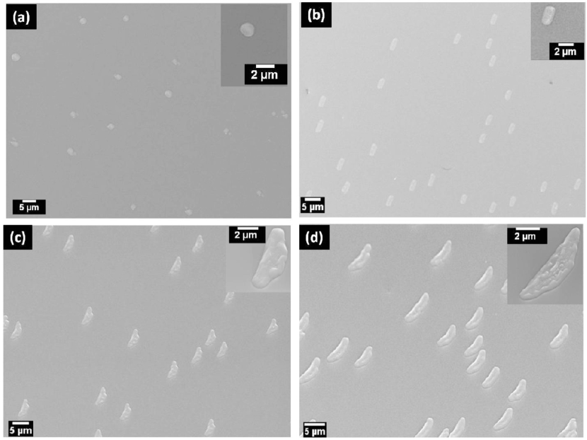
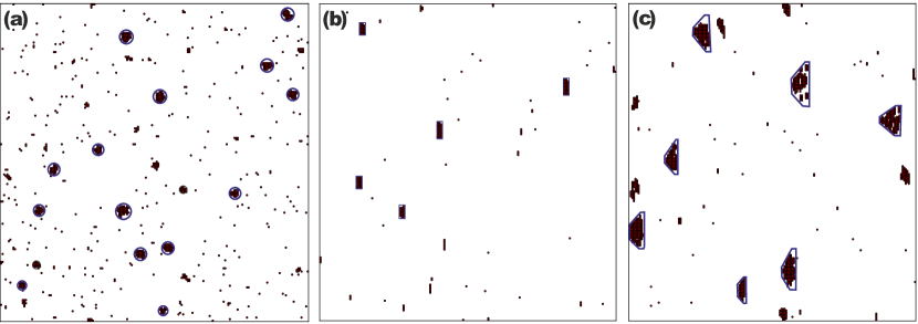
Figure 1 (a) and (b) depict the FEGSEM image for 2 ML and 5ML thick Ge film deposited on Si(5 5 12) substrate. As shown in Fig 1(a), the island structures are found to be spherical shape for a 2 ML Ge deposition, but for 5 ML Ge growth, rectangular island structures have been observed. For the 8ML and 10ML deposition cases, we observe trapezoidal structures [Fig.1(c),(d)]. It was reported earlier that DH is a necessary condition to form trapezoidal structural structures on Si(5 5 12) dash11 . The composition of these nanostructures has been characterized by using STEM - EDS dash11 ; dashmsm11 , Rutherford backscattering spectrometry (RBS)dash11 and the synchrotron-based high resolution x-ray diffraction (HRXRD). The HRXRD showed presence of graded Si1-xGex system for the Si(5 5 12)and is also confirmed by RBS measurements. While RBS measurements show no prominent graded Si1-xGex structures for the case of Si(5 5 3)and Si(5 5 7) substrate orientations.
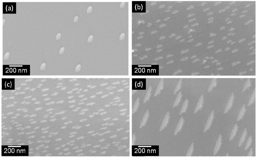
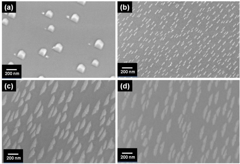
In fig.2, Ge growth of overlayer 3ML to 10ML on Si(5 5 7) has been shown where spherical nanoislands and rectangular nano rods are formed for 3ML and 5ML thicknesses[Fig.2(a),(b)] and nano trapezoid in the case of 8 ML and 10 ML Ge growth [Fig.2(c), (d)]. We have maintained the same growth condition for Si (5 5 3) substrate and seen that the growth kinetics and shape transformation follow in a similar way resulting from rectangular nano rod to nano trapezoid, as shown in fig.3.
We have measured the length and aspect ratio (length/width) of all the Ge-Si structures which has been shown in a tabular form in table 1 and table 2. In the case of Ge/Si (5 5 12) system, the size of the aligned structures are of micrometer size. But for the Si(5 5 7) and Si(5 5 3) systems,the size of the aligned structures are of nanometer size, though the shape evolution and also the aspect ratios are similar to that of Si(5 5 12) . From table 1, it is clearly seen that with increasing thickness, the size and aspect ratio of the Ge-Si structures increase accordingly. The aspect ratios of the Si-Ge elongated structures on Si( 5 5 12),Si(5 5 7) and Si(5 5 3) increase in a similar fashion as a function of increasing Ge growth coverages, which has been shown in table 2.
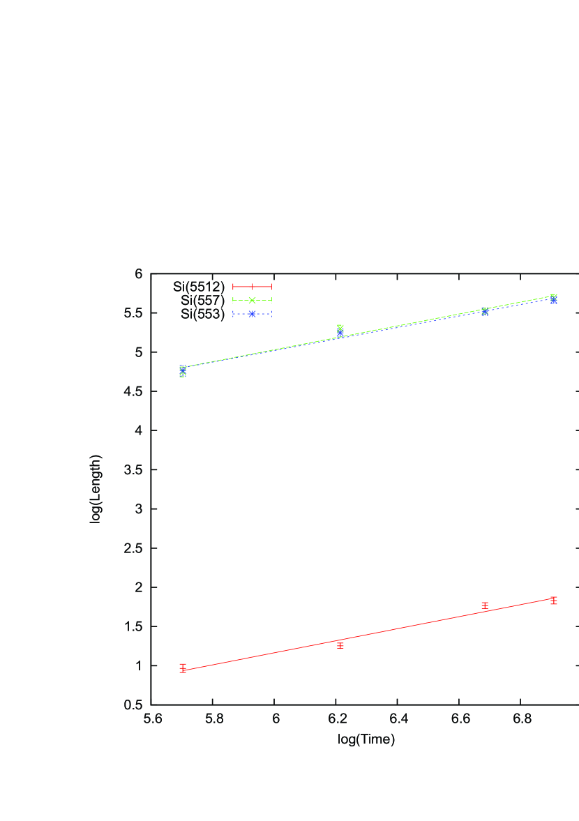
The growth of island followed a universality and we found from our experiments that the mean length of islands where is the time of deposition. The growth exponent from the experimental data is found to be about 0.75 0.02 for the case of the direct heating and 0.5 0.01 for the radiative heating case in all the three systems [table 3].We observe that since , the growth of island is sublinear. In fig 4, the log-log plot for size(length) vs deposition time shows almost same slope() irrespective of the size of the Si-Ge structures on the three substrates. We now disscuss the shape transformation of structures by kMC.
The kinetic Monte Carlo simulations were performed on a square lattice with . A coordinate system has been chosen such that the x-axis is directed along perpendicular to the step edges. We define horizontal bond and vertical bond as a pair of nearest neighbor atoms having the same y coordinates and same x coordinates respectively. Similarly a vertical bond is defined by a nearest neighbor pair of atoms with same x coordinates. The hopping rate of an adatom is given by
| (1) |
where is the Boltzman constant, is the temperature and is the vibrational frequency in the direction of the hopping. A typical value for our case is sec-1. The quantities , and denote the binding energies for the horizontal bond, vertical bond and the next nearest neighbor interaction respectively ; , and are the number of horizontal bonds, vertical bonds and the number of next nearest neighbors respectively and is a surface barrier term. For and , () constant, we obtained spherically symmetric island structures in the kMC simulation, since the binding energies are same for all bonds and surface barrier term is independent of direction. To obtain asymmetrical structures , we need to break the hopping symmetry. In our model, we introduce anisotropy through binding energies of different types of bonds and the dependence of surface barrier on the direction of hopping. For the isotropic cases, however, the hopping rate depends only on the nearest and next nearest neighbor interactions but does not depend on the specific arrangement of the neighboring atoms. In our experiment, the shape transformation has been observed when Ge is grown under DH condition dash11 . To simulate the experimentally observed shape variations, the surface barrier term is modified, so that it allows an asymmetric hopping of an adatom along the direction perpendicular to the step edge ( i.e. x direction). The values of along the step edges are same in both y directions. When and does not depend on the direction of hopping,spherical islands are formed. Symmetric elongated structures are formed for and uniform in all the directions of hopping. Trapezoidal islands can only be obtained when an asymmetric hopping term is present. The values of are defined as follows.a) for hopping along the positive x-direction, b) for hopping along the negative x-direction, c) for hopping along y-axis where depends only on the magnitude of the current (but for the simulations, this is a parameter only). Also so that the probabilities are strictly less than unity. Note that when , it reduces to the case of anisotropic island formation for as in the case of Ref.heyn01 and isotropic islands formation for as in Ref. lo99 .Therefore, in our kMC simulation a nonzero value of should correspond to the MBE growth done under DC heating. The mean shape of islands for this case is found to be trapezoids.
We follow the kMC algorithm in lo99 ; lo991 . We set the total coverage and the total number of Monte carlo steps . Particles are deposited at a constant flux . We define a dimensionless scale parameter , where is the surface energy barrier of the system when . This sets the time step for the simulation. An atom with empty adjacent site is called ’active’. An active atom is chosen at random and a single diffusion event is allowed to occur with a probability consistent with Eq.(1). If an atom is already there on the site to which it chooses to hop, then hopping fails. Time is incremented irrespective of whether the hopping is successful or not. The following parameters were used for our kMC : , and coverage is 2.5. It is important to note that the relative strength of the energy values is crucial in determining the shape of the structures. The above set of energy parameters is one such example.
In fig. 5 (a),spherical shaped islands for are seen. For , at coverage , rod like aligned structures formed [fig.5(b)]. Figure5 (c) is final snapshot of the trapezoidal structures formed at coverage for and . From the kMC simulation, we have found (for ) and (for ).
In summary,we report the shape evolution of MBE grown Si1-xGex islands on reconstructed high index Si(5 5 12), Si(5 5 7) and Si(5 5 3) surfaces. We show that a self assembled growth at optimum thickness leads to interesting shape transformations, namely, spherical islands to rectangular nanostructures and then to elongated trapezoidal structures. We have experimentally observed an universality in the growth of the islands for all three high index surfaces by evaluating the aspect ratios and growth exponent.The growth exponent (for the longer side of the structures) experimentally found to be about 0.75 0.02 for the case of the direct heating and 0.5 0.01 for the radiative heating case in all the three systems. Our kMC simulations show that such variations can be understood by introducing a deviation parameter in surface barrier term . The experimentally observed shape variations and the growth exponent values are in good agreement with kMC simulations. This suggests the role of stochastic process involved in the shape transitions of nanoscale structures. We thank S. D.Mohanty for stimulating discussions. PVS would like to thank the Department of Atomic Energy, Government of India for granting FEGSEM under 11th plan.
References
- (1) Y. Wu, R. Fan, and P. Yang, Nano Lett. 2, 83 (2002)
- (2) Minjoo L Lee, Eugene A Fitzgerald, Mayank T Bulsara, Matthew T Currie, and Anthony Lochtefeld J. Appl. Phys. 97, 011101 (2005)
- (3) Y -W Mo, D. E. Savage, B. S. Swartzentruber, and M. G. Lagally, Phys.Rev. Lett. 65 , 1020 (1990).
- (4) L. Persichetti, A. Sgarlata, M. Fanfoni, and A. Balzarotti, Phys.Rev. Lett. 104, 036104 (2010).
- (5) K. Ohmori, Y L Foo, S Hong, J G Wen, J E Greene, and I Petrov, Nano Lett. 5, 369 (2005).
- (6) Hidong Kim, Huiting Li, Jae M. Seo,Surf. Sci. 602, 2563 (2008).
- (7) I. Berbezier and A. Ronda,Phys. Rev. B 75, 195407 (2007).
- (8) A. A. Baski, S. C. Erwin, and E. J. Whiteman, Science 269,, 1556 (1995).
- (9) A. A. Baski, K. M. Saoud, and K. M. Jones, Applied Surf. Sci. 182, 216 (2001).
- (10) J. R. Ahn, Y. J. Kim, H. S. Lee, C. C. Hwang, B. S. Kim, and H.W. Yeom , Phys. Rev. B 66, 153403 (2002).
- (11) H. Kim,H Li,Yong-Zhe Zhu , J R Hann, and Jae M Seo,Surf. Sci. 601, 1831 (2007).
- (12) A. Kirakosian, R. Bennewitz, J. N. Crain, Th. Fauster, J -L Lin , D. Y. Petrovykh, and F. J. Himpsel Appl. Phys. Lett. 79, 1608 (2001).
- (13) Shinsuke HARA, Masamichi YOSHIMURA, and Kazuyuki UEDA, J. J. Appl. Phys. 47, 7 (2008)
- (14) J. Tersoff, and R. M. Tromp, Phys.Rev. Lett. 70, 2782 (1993).
- (15) D. J. Eahlesham, and M. Cerullo,Phys.Rev. Lett. 64, 1943 (1990)
- (16) Ch. Heyn, Phys. Rev. B 63, 033403 (2001)
- (17) K. E. Khor and S. Das Sarma, Phys. Rev. B 62, 16657 (2000)
- (18) K. A. Fichthorn, M. L. Merrick, M. Scheffier,Applied Phys. A. 75, 17 (2002)
- (19) D. K. Goswami, B. Satpati, P. V. Satyam, and B. N. Dev, Curr. Sci 84, 902 (2003)
- (20) J. K. Dash, A. Rath, R. R. Juluri, P. Santhana Raman, K. Müller, A. Rosenauer and P. V. Satyam,J.Phys. Condens. Matter 23, 135002 (2011).
- (21) J. K. Dash, A. Rath, R. R. Juluri, P. Santhana Raman, K. Müller, M. Schowalter, R. Imlau, A. Rosenauer, P.V. Satyam, J.Phys. Conf. Series 326, 012021 (2011).
- (22) Alan Lo and Rex T Skodje J.Chemical Phys. 111, 2726 (1999)
- (23) Alan Lo and Rex T Skodje J.Chemical Phys. 112, 1966 (1999)