Asymmetry to symmetry transition of Fano line-shape: Analytical description
Rajesh Kumar 111Corresponding authors: rajeshkumar@iiti.ac.in
Department of Physics, School of Basic Sciences, Indian Institute of Technology Indore, IET-DAVV Campus, Indore, Madgya Pradesh 452017, India
Abstract
An analytical description of Fano line-shape asymmetry ratio has been presented here for a general case. It is shown that Fano line-shape becomes less asymmetric as is increased and finally becomes completely symmetric in the limiting condition of q equal to infinity. Asymmetry ratios of Fano line-shapes have been calculated and are found to be in good consonance with the reported expressions for asymmetry ratio as a function of Fano parameter. Application of this derivation is also mentioned for explanation of asymmetry to symmetry transition of Fano line-shape in quantum confined silicon nanostructures.
Keywords: Electron-phonon interaction, Raman lineshape, Fano line-shape.
PACS No.: 78.67.f; 63.22.-m; 78.30.j
1 Introduction
Fano resonance [1] is a general property of the physical system where a degeneracy of continuum states and a discrete level raised into this continuum is present. Such a system is possible in simple systems like atoms [2], solids [3,4] as well as in complicated semiconductor systems like quantum heterostructures [5]. Fano resonance, also referred as Fano effect, can be observed in two different regimes namely linear and nonlinear. The linear regime is old and well understood and the effect is explained by classical theory given by Fano in his original paper [1]. Fano effect got importance after the observation of non-linear Fano effect very recently [6,7] in quantum systems. However the discussion will be limited to the classical Fano effect in this paper. In solid state, the Fano effect is understood in terms of electron-phonon interaction [8-10] provided the solid state system contains an available discrete level and a filled continuum of states. Apart from bulk materials, Fano effect has been observed in nanostructures [11-13] and heavily doped semiconductors [14-16]. In nanostructures, discrete phonons can interfere with continuum of electronic states available in the material as a result of quantum confinement [17-19]. On the other hand, in heavily doped semiconductors, the continuum of electronic states is available due to intra sub-band excitations possible due to Fermi level being pushed as a result of ultra-heavy doping in degenerate semiconductor [4,10,20,21]. Irrespective of the exact process, the result of this interaction is a characteristic asymmetric line-shape also known as Fano line-shape. Different properties of this line-shape is investigated to understand different physical systems. Understanding of Fano effect is important in exploring different fields of electronic transport [20,22] and spectroscopy [5,23]. Understanding this effect also helps in understanding different phenomena happening at microscopic level within the system [24]. One of the properties of this line shape is its asymmetry and the condition under which it becomes symmetry. This aspect will be dealt in this paper.
U. Fano in his classic observed this type of asymmetry in atomic systems [1]. He also indicated the possibility of this type of interaction in quantized discrete and continuous energy states. In other words, the Fano interaction can only be observed in systems where a discrete state is located within the continuum of different type of energy states. Semiconductors can be this type of classic system, where phonons have discrete energy states. The continuum of states may be provided by the electronic states under special conditions like heavy doping as in the case of degenerate semiconductors. Different conditions required for this type of interaction will be discussed in details in the following subsections. The possible Fano interaction between continuum of electronic states and discrete phonon state can be studied by Raman scattering [25,26] or IR spectroscopy [27]. The general properties of Fano effect can be understood by considering the special case of heavily doped Si [3,4,10,28,29] and ion-implanted Si [30], where Fano interaction is observed if the level of doping is of the order of cm-3, the semiconductor behaves like a degenerate semiconductor. Position of the Fermi level goes deep inside the conduction band, which gives rise to continuous electronic Raman scattering between the and bands along (100) directions [3,4]. A continuum of electronic transitions exists from a minimum energy () [10] to a maximum energy (). These extreme energies depend on the position of the Fermi level in the conduction band. In such systems, interference between a discrete phonon state and continuum of electronic states take place if the discrete optical phonons with energy satisfies the following condition given by eq. 1:
| (1) |
A system that satisfies the condition given in eq. 1, can show Fano-type asymmetric line-shape. If Raman spectroscopy is used to characterize the Fano effect, the generalized Raman line-shape as a result of Fano interaction can be written as following Eq. 2:
| (2) |
where with as the full width at half maxima (FWHM) and is the observed wavenumber of the Fano transition. The ‘’ is the Fano asymmetry parameter, which provides the measure of Fano interference. A low value of ‘’ means strong electron-phonon interaction. Asymmetric Raman line-shape is a signature of electron-phonon (Fano) interaction. Fano-type asymmetry in the Raman line-shape can be diagnosed by the following properties, which holds true for Fano line-shape. Upon varying the exciting laser wavelength, Raman peak position is unchanged whereas asymmetry parameter () increases with decreasing excitation wavelengh [10,31]. The interplay between value and the asymmetry of the line-shape is extremely important to understand a system showing Fano resonance. Aim of this paper is to give an analytic derivation to prove the asymmetry to symmetry conversion of Fano line-shape function.
2 Analysis and discussion
The Fano function given by Eq. 2 can be symmetric or asymmetric depending on the magnitude of with a maximum value at
| (3) |
As evident from this equation, Fano asymmetry parameter, , determines the peak position and asymmetry of the line-shape. Quantitatively asymmetry ratio is defined here as , where and are half widths on the low- and high-energy side of the maximum. The magnitude of decides the value of asymmetry whereas sign decides whether asymmetry is in higher wavenumber side or the lower side. In this paper, only positive values of is discussed in which case the Fano line-shape is wider in the higher wavenumber side. The Fano line-shape becomes symmetric for . This property of Fano line-shape can be seen experimentally as well as numerically.
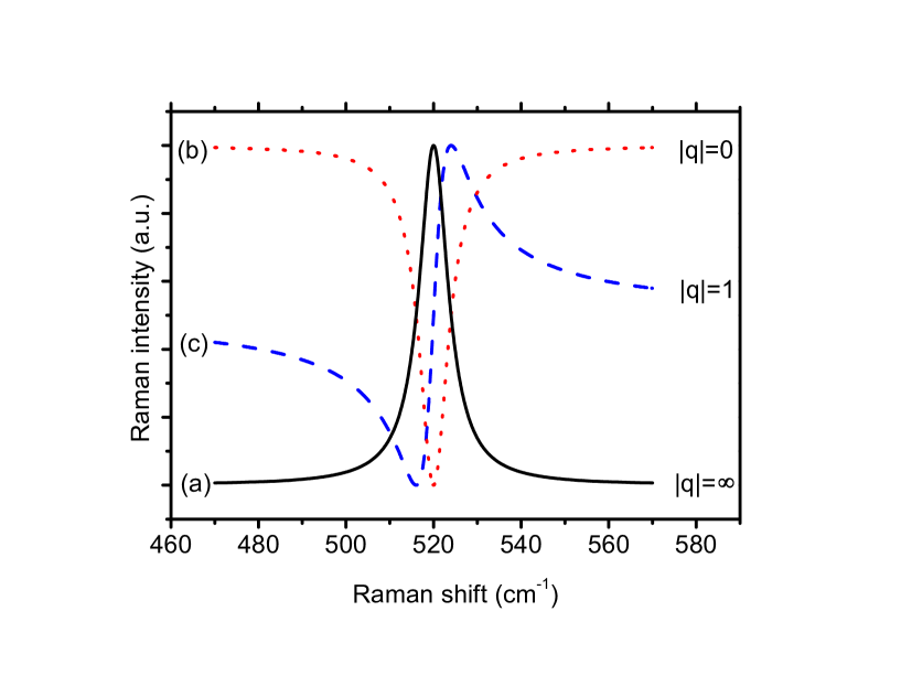
An analytic derivation for asymmetric to symmetric transition of line-shape given in Eq. 2 will be derived here to understand Fano effect in a better way. Figure 1 Shows a typical line-shape given by Eq. 2 for different values of . the value of and were taken as 520 cm-1and 8cm-1respectively. For , the curve is symmetric with peak at 520 cm-1as shown in figure 1(a). On the other hand, the Fano line-shape gets inverted by keeping the symmetry intact and shows a dip at 520 cm-1in stead of a peak as can be seen in figure 1(b). For intermediate value of =1, a typical Fano line shape can be seen in figure.1(c). However, figure 1(c) shows a maximum at 524 cm-1(value is consistent with eq. 3) asymmetry ratio can’t be defined for the same. On the other hand, the observation of minimum point at 516 cm-1is typical observation when 1. Observation of such minima in this regime is called the antiresonance [4] and is a characteristic of high Fano coupling.
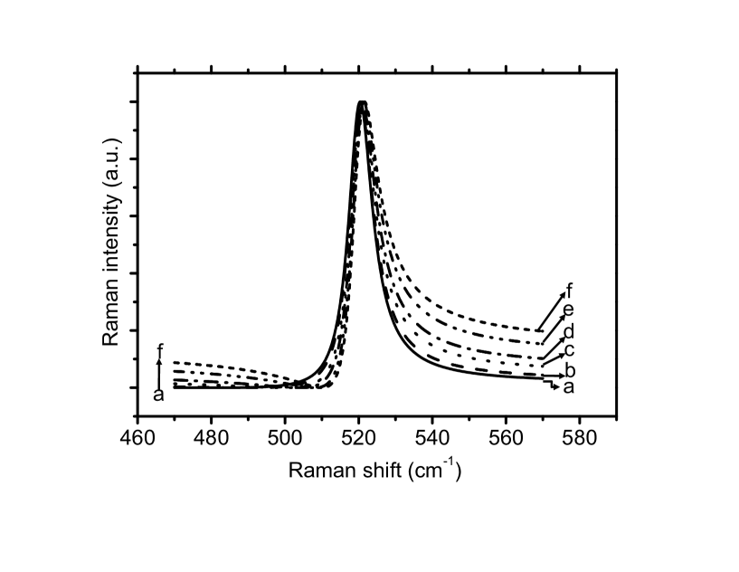
Figure 2(a) to 2(f) shows the line-shape given in Eq. 2 for different values of 2.5, 3, 4, 5, 7.5 and 10 respectively. A dependent asymmetry and antiresonance can be seen in figure 2 clearly. As the value of is decreasing (a to f), line-shape becomes more and more asymmetric with the curve getting broader on the higher wavenumber side. In other words, the Fano line-shape is less asymmetric for higher values of . This relationship can be derived as follows:
For, , in Eq. 2, and has a maximum value equal to . Since, is the FWHM which means and should be the points of equal intensities for the case of a near symmetric line-shape. Theoretically at and
| (4) |
Similarly, at and
| (5) |
From Eqs. (4) and (5), it is clear that intensity at and not equal. It means that the line-shape given by the Eq. (2) is asymmetric for . Thus the ratio of intensities at will be given by the Eq. (6) as follows.
| (6) |
| (7) |
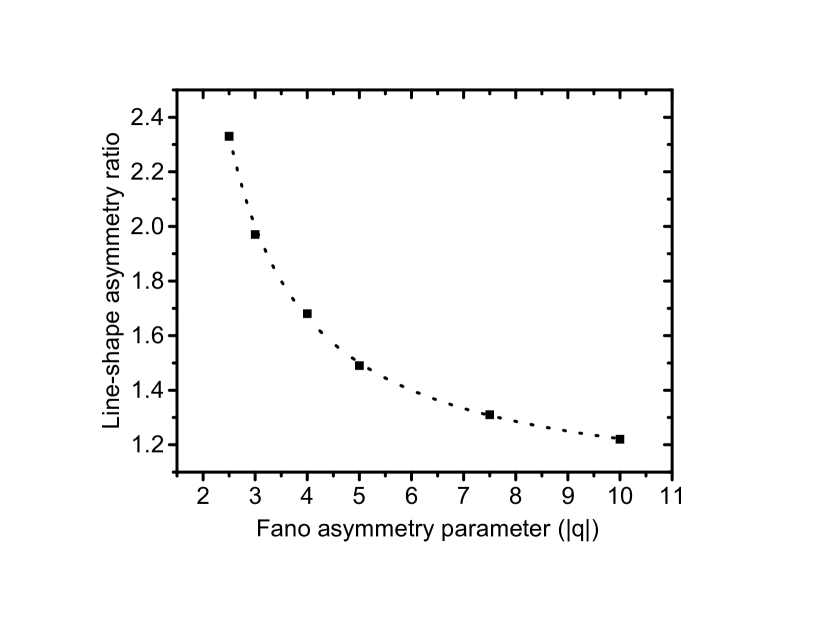
It is clear from Eq. (7) that for ‘’ tending to infinity, the Eq. (2) is symmetric in nature with FWHM of . This analytic derivation is consistent with theoretically plotted line-shapes. This property has been used in silicon nanostructures to explain the simultaneous observation of Fano effect and quantum confinement effect. In the work reported by Kumar et al [11], authors show that only quantum confinement effect is observed under control excitation condition to avoid any Fano effect. This observed fact is proved here analytically. Observed asymmetry ratio form line-shape in fig2 have been plotted as a function of Fano asymmetry parameter in figure 3 as solid points. The dotted line in figure 3 represents the theoretical asymmetry ratio of line-shape in eq 2. The line in figure 3 is expressed as eq. (8) [28] as follows:
| (8) |
Very good match between theoretically predicted and numerically calculated asymmetry ratios can be seen in figure 3. This match further confirms the fact that Fano line-shape in eq. 2 converges to symmetric one for low coupling regime characterized by higher values of .
3 Conclusion
Theoretical analysis of Fano line-shape asymmetry ratio show that Fano line-shape is asymmetric for Fano parameters () 1. The Fano-line shape is characterized by the point of antiresonance for 1. Calculated Fano line-shape show that Fano line-shape becomes less asymmetric as is increased and finally becomes completely symmetric in the limiting condition of equal to . This derivation has been used to explain the experimental observation of one of the old reports for the observation of photoexcited Fano interaction in silicon nanostructures.
References
- [1] U. Fano, Phys. Rev. 124, 1866-1878 (1961).
- [2] R. P. Madden and K. Codling, Phys. Rev. Lett. 10, 516-518 (1963).
- [3] F. Cerdeira and M. Cardona, Phys. Rev. B 5, 1440-1454 (1972).
- [4] M. Balkanski, K. P. Jain, R. Beserman, and M. Jouanne, Phys. Rev. B 12, 4328-4337 (1975).
- [5] S. Bar-Ad, P. Kner, M. V. Marquezini, S. Mukamel, and D. S. Chemla, Phys. Rev. Lett. 78, 1363-1366 (1997).
- [6] M. Kroner, A. O. Govorov, S. Remi, B. Biedermann, S. Seidl, A. Badolato, P. M. Petroff, W. Zhang, R. Barbour, B. D. Gerardot, R. J. Warburton, and K. Karrai, Nature 451, 311-314 (2008).
- [7] W. Zhang, A. O. Govorov, and G. W. Bryant, Phys. Rev. Lett. 97, 146804 (2006).
- [8] B. Parida, J. Sahoo, N. Shadangi, and P. Nayak, Indian J. Phys. 84, 1333-1339 (2010).
- [9] A. Srivastava, N. K. Gaur, and P. Bhardwaj, Indian J. Phys. 83, 437-445 (2009).
- [10] M. Chandrasekhar, J. B. Renucci, and M. Cardona, Phys. Rev. B 17, 1623-1633 (1978).
- [11] R. Kumar, H. S. Mavi, A. K. Shukla, and V. D. Vankar, J. Appl. Phys. 101, 064315 (2007).
- [12] R. Gupta, Q. Xiong, C. K. Adu, U. J. Kim, and P. C. Eklund, Nano Lett. 3, 627-631 (2003).
- [13] V. Magidson and R. Beserman, Phys. Rev. B 66, 195206 (2002).
- [14] Y. ying Wang, Z. hua Ni, T. Yu, Z. X. Shen, H. min Wang, Y. hong Wu, W. Chen, and A. T. Shen Wee, J. Phys. Chem. C 112, 10637-10640 (2008).
- [15] N. H. Nickel, P. Lengsfeld, and I. Sieber, Phys. Rev. B 61, 15558-15561 (2000).
- [16] N. Nakano, L. Marville, and R. Reif, Journal of Applied Physics 72, 3641-3647 (1992).
- [17] H. S. Mavi, A. K. Shukla, R. Kumar, S. Rath, B. Joshi, and S. S. Islam, Semicond. Sci. Technol. 21, 1627-1632 (2006).
- [18] R. Kumar, H. S. Mavi, and A. K. Shukla, Silicon 2, 25-31 (2010).
- [19] H. S. Mavi, S. Prusty, M. Kumar, R. Kumar, A. K. Shukla, and S. Rath, Phys. Status Solidi A-Appl. Mat. 203, 2444-2450 (2006).
- [20] H. Schmidt, K. L. Campman, A. C. Gossard, and A. Imamoglu, Appl. Phys. Lett. 70, 3455-3457 (1997).
- [21] F. Cerdeira, T. A. Fjeldly, and M. Cardona, Phys. Rev. B 8, 4734-4745 (1973).
- [22] J. Faist, F. Capasso, C. Sirtori, K. W. West, and L. N. Pfeiffer, Nature 390, 589-591 (1997).
- [23] J. Wagner and M. Cardona, Phys. Rev. B 32, 8071-8077 (1985).
- [24] R. Kumar and A. K. Shukla, Phys. Lett. A 373, 2882-2886 (2009).
- [25] C. V. Raman and K. S. Krishnan, Nature 121, 501-502 (1928).
- [26] C. Raman, Indian J. Phys. 02, 387 (1928).
- [27] H. J., Thin Solid Films 313-314, 656-660 (1998).
- [28] M. Jouanne, R. Beserman, I. Ipatova, and A. Subashiev, Solid State Communications 16, 1047-1049 (1975).
- [29] F. Cerdeira, T. A. Fjeldly, and M. Cardona, Phys. Rev. B 9, 4344-4350 (1974).
- [30] K. P. Jain, A. K. Shukla, S. C. Abbi, and M. Balkanski, Phys. Rev. B 32, 5464-5467 (1985).
- [31] F. Cerdeira, T. A. Fjeldly, and M. Cardona, Solid State Communications 13, 325-328 (1973).