Electronic and transport properties of azobenzene monolayer junctions as molecular switches
Abstract
We investigate from first-principles the change in transport properties of a two-dimensional azobenzene monolayer sandwiched between two Au electrodes that undergoes molecular switching. We focus on transport differences between a chemisorbed and physisorbed top monolayer-electrode contact. The conductance of the monolayer junction with a chemisorbed top contact is higher in trans configuration, in agreement with the previous theoretical predictions of one-dimensional single molecule junctions. However, with a physisorbed top contact, the ”ON” state with larger conductance is associated with the cis configuration due to a reduced effective tunneling pathway by switching from trans to cis, which successfully explains recently experimental measurements of azobenzene monolayer junctions. A simple model is developed to explain electron transmission across subsystems in the molecular junction. We also discuss the effects of monolayer packing density, molecule tilt angle, and contact geometry on the calculated transmission functions. In particular, we find that a tip-like contact with chemisorption significantly affects the electric current through the cis monolayer, leading to highly asymmetric current-voltage characteristics as well as large negative differential resistance behavior.
pacs:
85.65.+h,31.15.E-,73.50.-hI INTRODUCTION
Molecular junctions that incorporate photochromic molecules as reversible photo-switches between two different conductance states (”ON” and ”OFF”) have advanced considerably in the last decadeRussew:2009 ; Molen:2010 . Azobenzene and its derivatives are the most frequently studied candidates for photoresponsive molecular switch, based on their conformational changes from a more thermodynamically stable trans configuration to a cis configuration in response to an external stimulus such as UV lightChang:2004 , and vice versa upon exposure to visible light or thermal excitationIkegami:2003 . Previous first-principles studies for azobenzene molecular junctions focus on electron transport through ideal single-molecule junctions with one-dimensional (1D) electrodes and predict that the junction with trans configuration has a conductance higher than that with the cis configuration Zhang:2004 ; Zhang:2006 ; Valle:2007 .
More recent attention in experiments has been paid to the self-assembled monolayer (SAM) systems, which are highly ordered arrays of molecules on a two-dimensional (2D) surface with a chemisorbed bottom contact. A variety of experimental methods are used to apply a second contact on top of the azobenzene SAM and measure the photoinduced changes in its conductance, with sufficient flexibility to adapt to the height change of the SAM after its photo-switch, including liquid metal contact (eg., Hg drop Ferri:2008 ) and conducting atomic force microscopy Mativetsky:2008 ; Smaali:2010 . These pioneering experiments found that the ”ON” state with larger measured current is associated with the cis configuration, contrasting previous theoretical predictions based on single-molecule junction models.
These experiments using 2D monolayer junctions present more complicated situations in which the ideal 1D single-molecule junction model may not apply. First, in the monolayer junction the two monolayer-electrode contacts are not symmetric. The one at the bottom interface is a chemisorbed contact, in which the end group of the molecule is chemically bonded to the electrode. The top contact is merely physical, i.e., no chemical bonding formed between the SAM and the top electrode. It is known that the way the molecule interacts with the electrode plays a crucial role in electronic transport through the molecule. The conductance of a junction with and without chemicontacts can differ by several orders of magnitude Cui:2001 ; Taylor:2002 . In addition, SAMs can form with differences in packing density and tilt angle, and in densely packed SAMs the conductance may involve both intramolecular and intermolecular contribution due to molecules in close proximity Agapito:2008 . Other effects such as the surface topography and roughness of the contact also influence the final geometry of the contact and thus lead to more complex transport properties. These uncertainties in the microscopic details of a monolayer junction make understanding the effects of monolayer-electrode coupling, intermolecular interaction and contact geometries critical to elucidating its transport mechanisms. First-principles studies are especially valuable in this regard because information concerning the microscopic details of a monolayer junction and their effects on electron transport are often impossible to obtain directly in experiments.
Here we report a first-principles study of the electronic structure and transport properties of azobenzene monolayer junctions. The monolayer junction is constructed by attaching a Au(111) electrode on top of an azobenzene monolayer chemisorbed on Au(111) substrate. We focus on clarifying the role of monolayer-electrode bonding in relation to the transport properties by investigating the junctions with two types of top monolayer-electrode contact: 1) a strongly bonded contact in which the molecules are covalently bonded to the Au surface, and 2) a weakly bonded contact which is physisorbed through van der Waals (vdW) interation. We find that both the trans to cis transformation of the molecules and the monolayer-electrode bonding play critical roles in determining the electron transmission as well as the current-voltage characteristics of the monolayer junction. The impact of monolayer packing density and tilt angle are discussed. We also consider the effect of contact geometry by adding an additional Au atom at the top contact and find substantive changes in transport depending on this particular contact geometry.
II computational methods
We use two density functional theory (DFT) based computational methods in our calculations. First, all structural optimizations, including calculations for both the azobenzene monolayer on a Au(111) surface and the molecular junction consisting of two monolayer-electrode contacts, are performed using the plane-wave-basis-set Vienna ab initio simulation package (VASP) VASP:1996 . Then, electron transport calculations of the molecular junction are performed using the atomic-orbital-basis-set TRANSIESTA code Brandbyge:2002 , which incorporates nonequilibrium Green’s function formalism NEGF and DFT treatment of the electronic structure as implemented in the SIESTA package Soler:2002 .
In the structural optimization calculations, projector augmented wave potentials with kinetic energy cutoff of 400 eV are employed. For the exchange and correlation functional we utilize the Perdew-Burke-Ernzerh generalized gradient approximation (PBE-GGA) Perdew:1996 . A k-point sampling is applied based on the Monkhorst-Pack Monkhorst:1976 scheme. All geometries are optimized until the remaining force on each ion fall below the convergence criterion of 0.02 eV/Å.
In the electron transport calculations, we utilize norm-conserving nonlocal Troullier-Martins pseudopotentials and the PBE-GGA exchange correlation functional, with a single- plus polarization basis for the Au atoms and a higher level double- basis set for the molecules. The equivalent plane-wave cutoff for the real-space grid of 150 Ry is used throughout the calculations. A Monkhorst-Pack k-point sampling is used for self-consistent calculation, and a k-point sampling is used for transmission calculations. The transmission function is obtained by averaging transmission coefficients in each k-point for an applied bias voltage , , where
| (1) |
is the k-resolved transmission coefficient, are the retarded (advanced) Green’s function matrices, and where the are the retarded self-energies due to the existence of bottom (top) semi-infinite electrodes. The electric current as a function of the applied voltage is obtained by the integration of the transmission function
| (2) |
where is the elementary charge, is the Fermi-Dirac distribution function, are the chemical potentials for the bottom (top) electrodes.
III Azobenzene molecular monolayer on Au(111) surface
III.1 Structural models
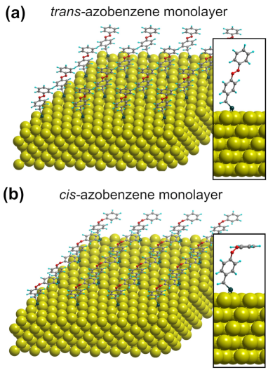
For the azobenzene monolayer on the Au(111) substrate (hereafter we denote this as Au-AB), the systems that we study consist of an azobenzene monolayer chemisorbed on the surface of Au(111) substrate by a linker for each molecule, as illustrated in Fig. 1 produced by VESTA graphical program Vesta3 . The substrate is modeled by a slab consisting of five Au(111) layers. The molecular coverage is kept fixed at one molecule per surface unit cell, which corresponds to a packing area of 90.8 per molecule. The supercell thus consists of 87 atoms comprising 12 atoms per Au layer and 27 atoms for the azobenzene molecule with the linker. A large vacuum spacing of 15 Å is used between the topmost molecular atom and the next Au slab to prevent interaction between adjacent images. All atoms except the two bottom Au layers are fully relaxed.
III.2 Adsorption geometry and energetics
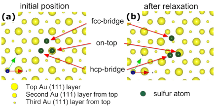
In order to determine the preferred adsorption position for the azobenzene monolayer on the Au(111) surface, three possible initial binding sites of both azobenzene isomers with the bottom linker are optimized on the Au(111) surface, the on-top site, the fcc- and hcp-bridge sites, as shown in Fig. 2. The calculated total energy and binding energy of an azobenzene molecule at different adsorption sites are reported in Table 1. For both trans and cis configurations, we find the most stable adsorption position to be the fcc-bridge site. We also find the trans configuration to be more stable by about 0.6 eV than the cis configuration, in good agreement with the results from previous calculations McNellis:2009 and experiment Schulze:1977 . Bader analysis based on the real-space charge density Henkelman:2006 for the Au-AB shows a small amount of charge transfer from Au substrate to the molecule for all cases, as given in Table 1. The charge transferred to the molecule is primary localized at the linker, and not efficiently shared with the core part of the molecule. Hereafter we present only the results for systems with the azobenzene monolayer chemisorbed on the fcc-bridge site of the Au(111) surface.
| isomer type | adsorption site | charge transfer | ||
|---|---|---|---|---|
| trans | fcc-bridge | 0 | 2.084 | 0.07 |
| hcp-bridge | 0.110 | 1.974 | 0.07 | |
| on-top | 0.398 | 1.686 | 0.08 | |
| cis | fcc-bridge | 0.635 | 2.112 | 0.08 |
| hcp-bridge | 0.700 | 2.037 | 0.07 | |
| on-top | 1.052 | 1.695 | 0.06 |
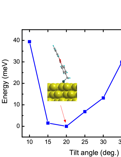
We also optimize the tilt angle of the azobenzene monolayer on Au(111) surface. In Fig. 3 we show the calculated total energy of a trans azobenzene monolayer on Au(111) as a function of tilt angle ranging from to . At every single energy point in Fig. 3, the monolayer structure is optimized by performing geometry relaxation with an initially given tilt angle. Within this angle range, we find that the lowest energy structure is the tilted molecular chemisorbed on the Au(111) surface. We expect the same finding for the cis configuration since the trans to cis transformation only change the geometry of top half of the azobenzene molecule. Therefore, for the rest of the study we choose azobenzene monolayer with tilt angle of as the equilibrium structure for both trans and cis configurations, as shown in Fig. 1.
However, it should be noted that in Fig. 3 the calculated total energies of these systems with different tilt angles are very close. In experiments, the tilt angle of molecules in the monolayer is usually determined by other factors, such as ambient temperature and monolayer packing density. It has been found that the molecular monolayer undergoes a phase transition from a tilted structure to a vertical structure at room temperature Alkis:2007 . Also, in densely packed monolayers at full coverage, monolayers with a small tilt angle can be generally expected, with molecules standing with their long molecular axes close to the surface normal.
III.3 Electronic structure
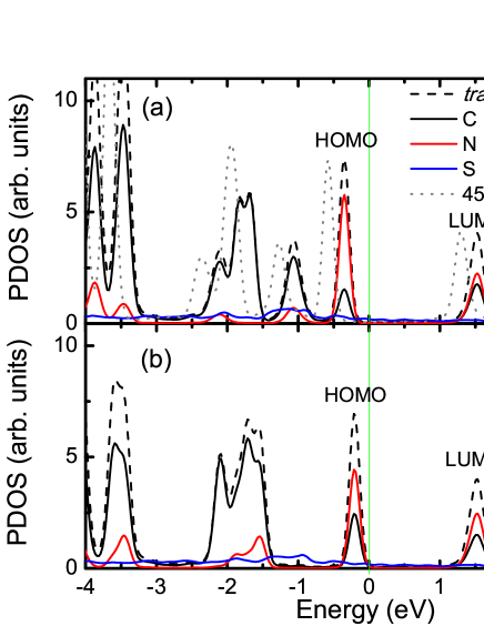
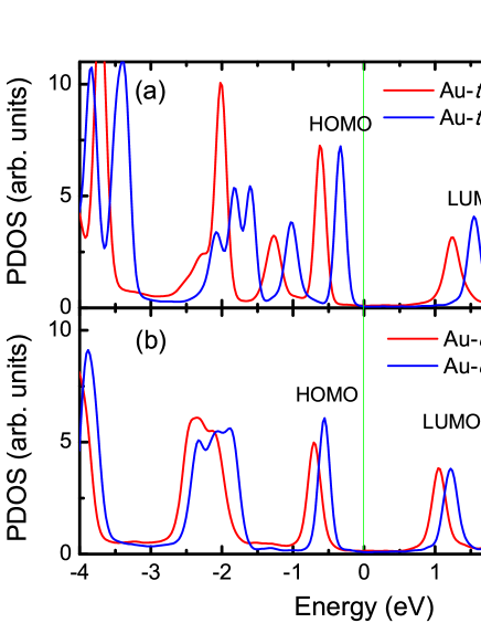
Figure 4 analyzes the interaction between the azobenzene and Au(111) surface in terms of the density of states projected onto the atoms (PDOS) in the molecule as well as the sulfur linker. For both trans and cis configurations, we see the two frontier orbital levels of azobenzene, highest occupied molecular orbital (HOMO) and lowest unoccupied molecular orbital (LUMO), lie at each side of the Au Fermi level. Unlike the other molecular orbital levels nearby, the HOMO and LUMO contain large contributions from the nitrogen pair of the azobenzene. The position of HOMO in the cis configuration is closer to the Au Fermi level than that in the trans configuration. This is quite different compared to the results from a study of a single azobenzene molecule on an Au(111) surface McNellis:2009 , in which the downshift of molecular orbital level is more significant for the cis isomer, resulting in the HOMO of cis azobenzene being away from the Au Fermi energy and its LUMO being very close to the Fermi energy. This difference arises because the azobenzene molecules in the monolayer are standing upright (nearly perpendicular to the surface), resulting in a weak interaction between the molecule and the bottom surface, whereas a single azobenzene molecule orients parallel to the surface and thus the closer proximity between the azo group (N pair) of the molecule and the Au surface creates a stronger interaction between them McNellis:2009 ; Chapman:2010 . For trans monolayer with a tilt angle of on the Au surface, we find essentially the same features in the PDOS as obtained for tilted trans monolayer, but all molecular orbital levels are roughly equally shifted by about 0.4 eV to lower energies.
IV Azobenzene monolayer junctions and transport properties
IV.1 Structural models and electronic structures
Once the equilibrium geometry of the Au-AB is obtained, we construct the corresponding molecular junction by extending the bottom Au(111) substrate into a six atomic layer slab, and attaching a second Au(111) slab consisting another six atomic Au layers on top of the azobenzene monolayer. To examine the effect of monolayer-electrode contact, two types of interfacial contacts for the top electrode are studied: (1) the top Au surface is covalently bonded to the azobenzen monolayer with linkers same as those at the bottom contact (hereafter we denote this type of junction as Au-AB-Au), and (2) the top contact is physisorbed on the azobenzene monolayer surface without the linkers (we denote this as Au-ABAu junction). We optimize the top interfacial contact by computing the total energies of the system as a function of the distance between the left and the right electrodes. Every single energy point is calculated by performing geometry optimization with a constrained electrode-electrode separation. Therefore the equilibrium geometry is obtained as the distance at which the total energy is minimal. Due to the failure of DFT GGA exchange correlation functionals to account for vdW interactions, we optimize the electrode-electrode separation using vdW density functionals optB88-vdW Klimes:2011 for junctions with physisorbed contacts. Fig. 6 (a) and (b) shows the optimized monolayer junction geometries with equilibrium electrode-electrode distance for trans and cis configurations, respectively.
We show the PDOS of the azobenzene molecules in the monolayer junctions in Fig. 5. As compared to the PDOS of the bare monolayer on Au(111) surface, it can be clearly seen that all molecular orbital levels, including the HOMO and the LUMO, are shifted to lower energies with the presence of a top monolayer-electrode contact. In Fig. 5 (a), the downshift of molecule orbital levels in the Au-transABAu junction is only minimal, as compared to Fig. 4 (a), primarily because of a weak bonding between the top electrode and the transAB molecule. In contrast, with the sulfur linkers in the top contact of the Au-transAB-Au junction, a stronger monolayer-electrode bonding significantly lower all molecular orbital levels in energies by about 0.3 eV. The downshift is even more significant in the cases of cis configurations as shown in Fig. 5 (b). All cis azobenzene orbital levels shift to lower energies by about 0.4 eV in Au-cisABAu and 0.6 eV in Au-cisAB-Au, compared to Fig. 4 (b).
IV.2 Transmission functions at zero-bias
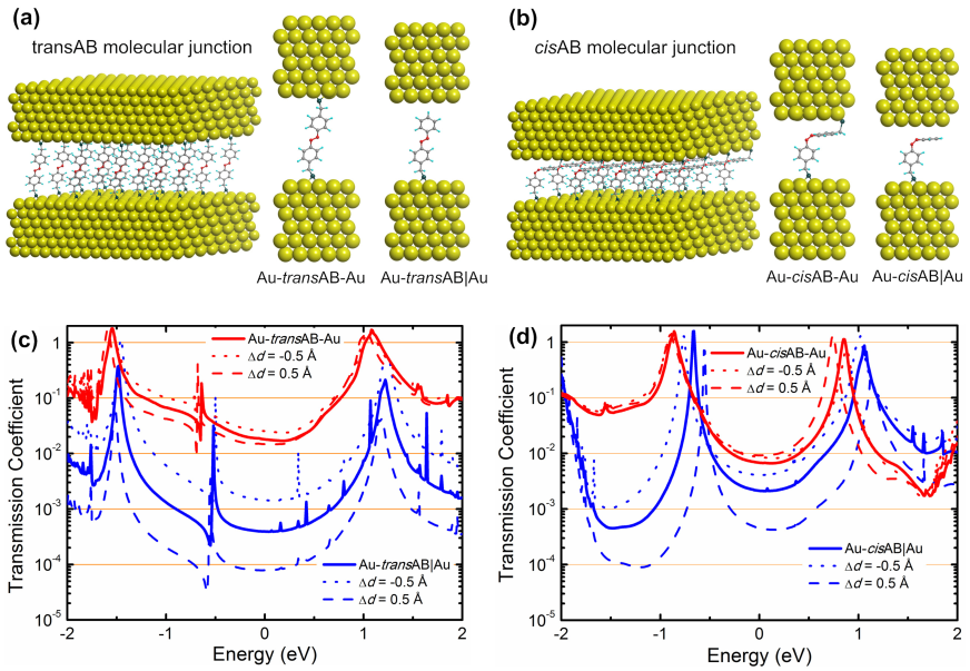
In Fig. 6 (c) and (d) we show the calculated transmission functions at zero-bias for azobenzene monolayer junctions with trans and cis configurations, respectively. For the Au-transAB-Au junction with chemisorbed top contact, transmission function has three broad resonance peaks with near perfect transmission amplitudes shown in the given range of energy from -2 eV to 2 eV related to the Fermi energy of the Au electrodes: two are below the Fermi energy (about -1.6 eV and -0.7 eV), and the third is above it (about 1.1 eV). These three transmission peaks can be directly associated to the frontier molecular orbitals HOMO-1, HOMO and LUMO, respectively, despite some minor changes in the energy as compared to the PDOS in Fig. 5 due to the periodic boundary condition used in the supercell calculation for PDOS. The transmission peak associated with the HOMO of trans azobenzene is relatively narrower in width and lower in height because of the fact that the HOMO is more localized in the N pair of the molecule and thus contributes less to the electron transmission. These resonance peaks in the transmission function are away from the Au Fermi level, and zero-bias conductance of the monolayer junction is primarily dominated by non-resonance electron tunneling at the Fermi level, with a transmission coefficient . For the Au-transABAu junction with a physisorbed top contact, we find that the calculated transmission function is significantly decreased by about two orders of magnitudes as compared to that of Au-transAB-Au junction, and, at the Fermi level, . The resonance transmission peaks of Au-transABAu junction shift about 0.2 eV upward in the energy, which follows closely the peaks in PDOS as shown in Fig. 4 (a). Besides three major peaks, there are several small resonance peaks appearing in the transmission function of Au-transABAu around 0 eV to 1.2 eV which are induced by the vacuum gap in the top contact. Their relatively smaller amplitudes provides only finite contribution to the tunneling current under certain bias voltages, which we will discuss later in the next section.
For monolayer junctions with cis configuration, however, removing the linkers in the top contact leads to a relatively much smaller decrease in transmission function near the Fermi energy, as shown in Fig. 6 (d). The transmission functions at the Fermi level for junctions Au-cisAB-Au and Au-cisABAu are and 0.002, respectively. For both Au-cisAB-Au and Au-cisABAu, within the given range of energy two resonance peaks can be found in the transmission functions, which are associated with the cis azobenzene HOMO and LUMO. They are also away from the Au Fermi level, and the peaks of Au-cisAB-Au junction are lower in energy than that of Au-cisABAu, corresponding to the PDOS peaks as shown in Fig. 4 (b).
The above calculated zero-bias transmission function cannot be simply studied by its relation to the electrode-electrode separation or the azobenzene molecular length. Instead, we can describe the total transmission function that reflects the efficiency of electronic transport from one electrode to the other through the azobenzene monolayer junction as
| (3) |
where and give the efficiency of electron transport across the bottom and top contacts, and and reflect the electron transport through the first (bottom half) and second (top half) parts of the azobenzene molecule, respectively. From Fig. 6 (a) and (b), it is safe to assume that the first term in the above transmission equation is the same for all four junctions. However, the other three terms, , and , are quite different from case to case, resulting in different total transmission coefficients at the Fermi energy for the above junctions. In the case of the symmetric Au-transAB-Au junction, we have and , and the junction has a large transmission coefficient at the Fermi level, . The absence of the linker in the Au-transABAu junction causes a large decrease in , and reduces the total transmission coefficient to . One may expect such a large change in the transmission term to also apply to the cis configuration junction. However, as shown in Fig. 6 (d), the total transmission coefficient for Au-cisABAu () is only about three times smaller than that for Au-cisAB-Au (). This clearly indicate that, in the Au-cisABAu junction, the transmitted electron travel directly from the bottom contact to the top contact through only the first (bottom) part of the cis azobenzene molecule, and avoid the second (top) part of the molecule. Thus for the Au-cisABAu junction the effective tunneling pathway is greatly reduced, resulting a total transmission function . Note this is equal to Eq. 3 with term that compensates the smaller term of the Au-cisABAu junction, resulting in a smaller difference in the total transmission coefficients between the Au-cisABAu and Au-cisAB-Au junctions as compared to that of the junctions in the trans configuration.
It should be also noted that the transmission terms and are also different between junctions with trans and cis configurations. Non-resonant electron transmission through a molecule can be empirically expressed as , where is the length of the molecule and represents the width of effective tunneling barrier, and is the tunneling decay factor given by where is the barrier height for tunneling that is determined by the frontier molecular orbital level related to the Fermi energy, , is the effective mass and is the shape constant of the barrier. For junctions with chemisorbed top contact, at the Fermi energy the total transmission ratio between trans and cis configurations is . Giving from Fig. 6 and estimated from the length of each half of the azobenzene molecule (remain unchanged upon switching), we have . For junctions with physisorbed top contact, from the above discussions we know that in the Au-transABAu the effective barrier width for the expression of is and that in Au-cisABAu is , thus the total transmission ratio between these two junctions at the Fermi energy should be . Giving from Fig. 6, we get the tunneling decay factors and . Both of them are in good agreement with the literature values () commonly obtained for short -conjugated molecules Salomon:2003 . A possible cause for a smaller tunneling decay factor than could be the fact that the HOMO level of junction in the trans configuration lie closer to the Fermi level than the HOMO level of the junction in the cis configuration, as shown in Fig. 5 and Fig. 6, resulting in a lower tunneling barrier, . The barrier shape constant could also be affected after the switching of azobenzene monolayer from trans to cis form.
In experiments, the monolayer-electrode contact of the junction may not be exactly at its equilibrium position, but rather be slightly stretched or compressed. To simulate this situation, we calculate the transport properties of junctions with an increased (or decreased) electrode-electrode separation (or ) with regard to its equilibrium value () for both trans and cis monolayer junctions. The transmission results for stretched and compressed junctions are also shown in Fig. 6. We find that the conductance of the Au-AB-Au junction with chemisobed top contact is insensitive to the change of for both trans and cis configurations, where as for Au-ABAu junctions with physisobed top contact, a small change in the electrode-electrode separation in either direction changes the conductance significantly. This demonstrates that, with a physisorbed top contact, the total transmission function of the monolayer junction is highly related to the (contribution from the contact) which is very sensitive to the monolayer-electrode contact distance. In the case of Au-cisABAu junctions, we also notice that the two peaks in the transmission function at about -0.7 eV and 1.1 eV, which are associated with the HOMO and the LUMO, move up in energy with increased electrode-electrode separation. This phenomenon has also been noticed for other stretched molecular junctions Xue:2003 , in which the shift of HOMO resonance in the transmission function toward the Fermi level increases the transmission coefficient at the Fermi energy. However, here the decrease in the transmission coefficient at the Fermi level, due to the stretching of the junction, is much more significant. The transmission peak associated with the cis HOMO is still more than 0.5 eV away from the Fermi level with , making the decrease in low bias conductance unlikely to be compensated. In contrast, for stretched and compressed Au-transABAu junctions we do not see such obvious change in the positions of transmission resonances.
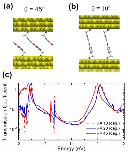
In order to understand the possible influences of the monolayer tilt angle on the transport properties, we carry out further calculations for Au-transAB-Au junction with different . The optimized junction structures with or tilted trans monolayer are shown in Fig. 7 (a) and (b), respectively. A large change in the electrode-electrode separation occurs between these two cases (). However, as shown in Fig. 7 (c), for junctions with a or tilted trans monolayer, we find essentially the same features in the transmission functions as those obtained for the optimized geometry with , yet with a small change in position of transmission resonance peaks associated with the trans azobenzene molecular orbital levels for . The transmission at the Fermi level for tilted junction is only slightly increased as compared to the junctions with small tilt angles. The source of this increase is the downward shifting of the broad peak in the transmission function associated with the trans LUMO. The shifting of molecular frontier levels resulting from the change in tilt angle may be resulted from a change in the effective dipole moment as well as the work-function at the molecule-metal interfaces Renzi:2005 . Similar phenomena have also been noticed in tilted alkanethiol monolayers Frederiksen:2009 , in which the tilt brings the HOMO resonance closer to the Fermi energy. Nevertheless, we conclude that for dilute monolayer junctions without intermolecular contribution, the molecular tilt has very little effect on its conductance since the effective tunneling pathway through the molecule remains unchanged upon tilting.
IV.3 Current-voltage characteristics
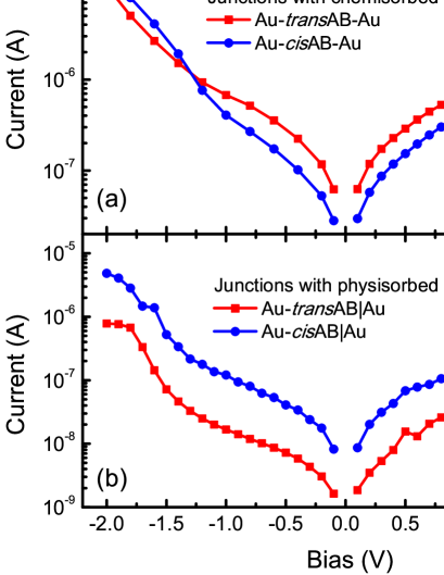
The self-consistently calculated current-voltage characteristics (I-V) of Au-AB-Au and Au-ABAu junctions are depicted in Fig. 8 (a) and (b), respectively. For the Au-transAB-Au junction, a highly symmetric I-V curve arises as expected with two symmetric monolayer-electrode contacts, and its current is larger than that of the Au-cisAB-Au junction in small bias region, consistent with the zero-bias transmission functions. Thus, with chemisorbed top contact, the two isomers realize different conductance states of the monolayer junction corresponding to “ON” (trans configuration) and “OFF” (cis configuration). The current of the Au-transAB-Au junction becomes smaller than that of the Au-cisAB-Au only in the region of large negative bias voltage (-1.2 V to -2.0 V). This can be attributed to the fact that the Au-cisAB-Au junction is asymmetric in geometry, resulting in an asymmetric I-V curve which has a slightly larger current in the large negative bias region. Such asymmetric behavior is also shown in the I-V curves for junctions Au-transABAu and Au-cisABAu, with asymmetric top (physisorbed) and bottom (chemisorbed) contacts. Nonetheless, for junctions with a physisorbed top contact, the cis configuration (“ON” state) exhibits a larger current for any given voltage than that of the trans configuration (“OFF” state), and the ON/OFF ratio of the current is more pronounced than that of the junctions with chemisorbed top contacts. These theoretical results for junctions with a physisorbed top contact are, therefore, in reasonable qualitative consistency with the reported measurements Ferri:2008 ; Mativetsky:2008 ; Smaali:2010 . A quantitative matching of the ON/OFF ratio to the experiments is not expected because the length of the molecules in experiments are much longer than those in our study.
In Fig. 8 (b), we find the current of the Au-transABAu junction oscillates as a function of positive bias voltage, which correspond to the small resonance peaks found in the transmission function above the Fermi level as shown in Fig. 6 (c). As we increase the voltage, these resonance peaks sequentially join the bias window and contribute to the current, resulting in resonant tunneling current at certain bias voltages. However, these resonances can only provide finite contribution to the current in the trans configuration and the current ratio between the trans and cis configurations is almost unaffected.
IV.4 Effect of molecular packing density
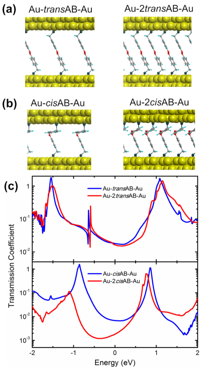
The above calculations are based on a diluted monolayer structure with a low packing density, in which the intermolecular bonding between molecules in the monolayer can be considered negligible and junction transport properties are primarily dominated by the intramolecular contribution. To inquire into effect of intermolecular interaction on the transport, Au-AB-Au junctions with a higher monolayer packing density are also considered, in which the molecules are positioned closer to each other to increase the molecular interactions. In this case for each junction we have two azobenzene molecules per Au(111) unit cell, and the packing area corresponds to 45.4 per molecule. The optimized junction structures for trans and cis configurations are shown in Fig. 9 (a) and (b), and we denote them as Au-2transAB-Au and Au-2cisAB-Au, respectively. For the cis configuration, as compared to the Au-cisAB-Au junction with a low packing density, we see that the azobenzene molecules in the monolayer of the Au-2cisAB-Au junction become distorted, so that the top half of the molecule is no longer parallel to the top Au surface but instead rotated relative to the Au surface, resulting from an increased intermolecular interaction with decreased spacing between the molecules.
The calculated zero-bias transmission functions are shown in Fig. 9 (c). For the trans configuration, doubling the packing density produces only negligible changes in transmission function. However, for the cis configuration, the junction’s transmission coefficients are significantly reduced especially in the energy region around the Fermi level. The decrease in conductance by increasing the packing density has also been observed in other monolayer junctions Agapito:2008 , but the reason has been attributed to a shift of the LUMO resonance peak in the transmission function to a higher energy away from the Fermi level. Our result differ from the Ref. Agapito:2008, in that the LUMO peak in the transmission function of the Au-2cisAB-Au junction slightly shifts to a lower energy which is closer to the Fermi level as compared to the Au-cisAB-Au. Nevertheless, the transmission coefficients for the HOMO resonance peak and for the energy region around the Fermi level are decreased by about one order of magnitude. The considerable decrease in the transmission function can be attributed to the geometry distortion in the cis azobenzene monolayer which is caused by intermolecular interactions with the dense packing, as shown in Fig. 9 (b). Our results show clearly that interaction among the azobenzene molecules of the monolayer junction can induce large changes in transport in the cis configuration, hence suggesting that higher conductance ON/OFF ratio can be achieved in densely packed azobenzene monolayer junctions with chemisorbed monolayer-electrode contact. For junctions with a physisorbed contact, since the “ON” state is associated with the cis configuration, we expect that increasing the monolayer packing density could decrease the conductance ON/OFF ratio.
IV.5 Effect of top-contact geometry
Having addressed the transport properties of azobenzene molecular junctions with a perfect contact surface at the monolayer-electrode interface, it is necessary to also study the consequences of non-ideal situations. To investigate the role of contact atomic structure, we consider a simple but possible situation: the sulfur atom bound to a single Au atom protruding from the surface of the top Au electrode, which is shown in Fig. 10 (a) and (b) for trans and cis configurations, and we denote them as denoted as Au-AB--Au and Au-2cisAB-Au, respectively. The purpose of this consideration is to simulate possible situations in experiments in which the surface of top electrode may not be atomically flat when contacting the molecules in the monolayer.
The calculated transmission functions are shown in Fig. 10 (c). We find that the additional Au atom decreases the transmission coefficients at non-resonance tunneling regions in the transmission function for both trans and cis configurations, as compared to Fig. 6. Moreover, the resonance peaks in the transmission functions associated with the frontier molecular orbitals, all shift up in energy at a noticeable change. The HOMO transmission resonance of Au-transAB--Au junction shifts from -0.7 eV to -0.4 eV; while that of Au-cisAB-Au junction shifts from -0.85 eV to -0.2 eV, which is very close to the Fermi energy.
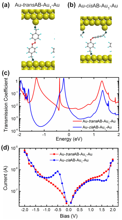
In Fig. 10 (d) we show the calculated current-voltage characteristics for Au-AB--Au junctions. The most noticeable feature appearing in Fig. 10 (d) is the asymmetry in the cis configuration. For a negative bias voltage below 1 eV, the current through the cis configuration is significantly higher than the current through the trans configuration. As the negative bias is further increased, the current through the cis configuration decreases dramatically with increasing voltage, resulting in a region of negative differential resistance (NDR). This NDR feature also appears in the positive bias region (from 1.2 V to 1.7 V) in the cis configuration, but is not present for any bias region in the trans configuration. In contrast to Au-cisAB--Au, the - characteristics of Au-transAB--Au junction are basically unchanged by the presence of the additional Au atom as compared to Fig. 8 (a).
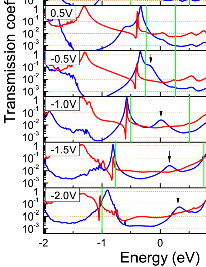
To shed light on the origin of the NDR effect, we give the transmission function at a series of biases from to 2.0 V at 0.5 V intervals as shown in Fig. 11. In the case of the cis configuration, a voltage of V creates a bias-induced transmission peak at about eV (marked with an arrow in Fig. 11) adjacent to the resonance peak associated with molecular LUMO. As the negative bias is further increased, this transmission peak, with a broad width, moves up in energy and towards the molecular LUMO resonance. It dominates the transmission function within the bias window, thus raising a much larger current than that at positive bias and resulting in a noticeable rectification effect for Au-cisAB--Au junction in Fig. 10 (c). In the case of trans configuration, however, only several bias-induced transmission peaks exist at positive bias, and all of them have much lower amplitudes and shorter width leading to only small current contributions. Correspondingly, in Fig. 10 (c) the rectification behavior in the I-V curve of Au-transAB--Au junction is not obvious and there is no NDR effect. This demonstrate that the azobenezene monolayer junction can be used for photo-controlled molecular rectifier with proper engineering of its contact geometry.
It should also be noted that for both trans and cis configurations, the bias drives the LUMO resonance peak away from the Fermi level, so its contribution to the current becomes important only at a sufficiently large bias (e.g. V) which should be comparable to the HOMO-LUMO gap of the molecule. This is also true for the calculated - characteristics in Sec. IV.3. Therefore, at low bias the electronic transport of all the monolayer junctions in consideration is mainly facilitated by non-resonant electron tunneling.
V Conclusion
Our first-principles calculations indicate that monolayer-electrode bonding, intermolecular interaction, and contact geometry all play very important roles in determining the conductance ratio of azobenene monolayer junction between trans and cis configurations. With a strongly bonded top contact from chemisorption, the zero-bias transmission of trans monolayer is higher than that of the cis monolayer. Replacing it by a weakly bonded contact with physisorption will decrease the conductance by about two orders of magnitudes for the trans monolayer. However, in the case of the cis configuration, the physisorbed contact shortens the effective tunneling pathway, leading to a conductance that is less sensitive to weak bonding. The mechanism are interpreted by applying a simple transmission model to the calculated zero-bias transmission functions, which accounts for electron transmission through each subunit of the molecular junction and provides a clear physical picture for understanding the junction. The calculated current-voltage characteristics indicate that, for junctions with physisorbed top contact, the ”ON” state with larger current is associated with the cis configuration, which are in agreement with recent experiments. Our calculations demonstrate the intermolecular interaction in the trans configuration is negligible even in a densely packed monolayer; while for cis configuration increasing the monolayer density causes a considerable distortion in the monolayer structure, resulting a decrease in its transmission function thus increasing the conductance ratio. We also find that the calculated current-voltage characteristics for the trans monolayer remain symmetric upon changing of the top contact geometry. In contrast, a slightly modified contact geometry will affect the electric current through the cis monolayer, leading to a highly unsymmetrical current-voltage curve as well as a large negative differential resistance behavior. These results suggest that the molecule-lead contact, the state of the molecule, the morphology of the metal surface, and the packing density of the monolayer are all parameters in the play. Our investigations thus will deepen understanding electron transport through azobenzene monolayer junctions.
This work is supported by US/DOE/BES/DE-FG02-02ER45995. The authors acknowledge DOE/NERSC and UF-HPC centers for providing computational resources.
References
- (1) M.-M. Russew, S. Hecht, Adv. Mater. 22, 3348 (2010).
- (2) S. J. Molen and P. Liljeroth, J. Phys. Condens. Matter 22 133001 (2010).
- (3) C.-W. Chang, Y.-C. Lu, T.-T Wang, and E.W.-G. Diau, J. Am. Chem. Soc. 126, 10109 (2004).
- (4) T. Ikegami, N. Kurita, H. Sekino, and Y. Ishikawa, J. Phys. Chem. A 107, 4555 (2003).
- (5) C. Zhang, M.-H. Du, H.-P. Cheng, X.-G. Zhang, A. E. Roitberg, and J. L. Krause, Phys. Rev. Lett. 92, 158301 (2004).
- (6) C. Zhang, Y. He, H.-P. Cheng, Y. Xue, M. A. Ratner, X.-G. Zhang and P. Krstic, Phys. Rev. B 73, 125445 (2006).
- (7) M. Valle, R. Gutiérrez, C. Tejedor, and G. Cuniberti, Nat. Nanotechnol. 2, 176 (2007).
- (8) V. Ferri, M. Elbing, G. Pace, M. D. Dickey, M. Zharnikov, P. Samori, M. Mayor, and M. A. Rampi, Angew. Chem. Int. Ed., 47, 3407 (2008).
- (9) J. M. Mativetsky, G. Pace, M. Elbing, M. A. Rampi, M. Mayor and P. Samori, J. Am. Chem. Soc. 130, 9192 (2008).
- (10) K. Smaali, S. Lenfant, S. Karpe, M. Oçfrain, Philippe Blanchard, D. Deresmes, S. Godey, A. Rochefort, J. Roncali, and D. Vuillaume, ACS Nano, 4, 2411 (2010).
- (11) X. D. Cui, A. Primak, X. Zarate, J. Tomfohr, O. F. Sankey, A. L. Moore, T. A. Moore, D. Gust, G. Harris, and S. M. Lindsay, Science 294 571 (2001).
- (12) J. Taylor, M. Brandbyge, and K. Stokbro, Phys. Rev. Lett. 89, 138301 (2002).
- (13) L. A. Agapito, C. Cao, and H.-P. Cheng, Phys. Rev. B 78, 155421 (2008).
- (14) G. Kresse and J. Furthmüller, Comput. Mat. Sci. 6, 15 (1996).
- (15) M. Brandbyge, J. L. Mozos, P. Ordejón, J. Taylor, and K. Stokbro, Phys. Rev. B 65, 165401 (2002).
- (16) S. Datta, Electronic Transport in Mesoscopic Systems (Cambridge University Press, Cambridge, England, 1995).
- (17) J. M. Soler, E. Artacho, J. D Gale, A. García, J. Junquera, Pablo Ordejón and D. Sánchez-Portal, J. Phys.: Condens. Matter 14, 2745 (2002).
- (18) J. P. Perdew, K. Burke, and M. Ernzerhof, Phys. Rev. Lett. 77, 3865 (1996).
- (19) H. J. Monkhorst and J. D. Pack, Phys. Rev. B 13, 5188 (1976).
- (20) K. Momma and F. Izumi, J. Appl. Crystallogr. 44, 1272 (2011).
- (21) E. McNellis, J. Meyer, A. D. Baghi, and K. Reuter, Phys. Rev. B 80, 035414 (2009).
- (22) F. W. Schulze, H. J. Petrick, H. K. Cammenga, and H. Klinge, Z. Phys. Chem., Neue Folge 107, 1 (1977).
- (23) G. Henkelman, A. Arnaldsson, and H. Jónsson, Comput. Mater. Sci. 36, 254-360 (2006).
- (24) S. Alkis, P. Jiang, L.-L. Wang, A. E. Roitberg, H.-P. Cheng, and J. L. Krause, J. Phys. Chem. C 111, 14743 (2007).
- (25) C. Chapman and I. Paci, J. Phys. Chem. C 114, 20556 (2010).
- (26) J. Klimeš, D. R. Bowler, and A. Michaelides, Phys. Rev. B 83, 195131 (2011).
- (27) A. Salomon, D. Cahen, S. Lindsay, J. Tomfohr, V.B. Engelkes, C.D. Frisbie, Adv. Mater. 15, 1881 (2003).
- (28) Y. Xue and M. A. Ratner, Phys. Rev. B 68, 115407 (2003).
- (29) V. De Renzi, R. Rousseau, D. Marchetto, R. Biagi, S. Scandolo, and U. del Pennino, Phys. Rev. Lett. 95, 046804 (2005).
- (30) T. Frederiksen, C. Munuera, C. Ocal, M. Brandbyge, M. Paulsson, D. Sanchez-Portal, and A. Arnau, ACS Nano, 3, 2073 (2009).