reprintrevtex4-1
Voltage sensing in ion channels:
Mesoscale simulations of biological devices
Abstract
Electrical signaling via voltage-gated ion channels depends upon the function of a voltage sensor (VS), identified with the S1–S4 domain in voltage-gated K+ channels. Here we investigate some energetic aspects of the sliding-helix model of the VS using simulations based on VS charges, linear dielectrics and whole-body motion. Model electrostatics in voltage-clamped boundary conditions are solved using a boundary element method. The statistical mechanical consequences of the electrostatic configurational energy are computed to gain insight into the sliding-helix mechanism and to predict experimentally measured ensemble properties such as gating charge displaced by an applied voltage. Those consequences and ensemble properties are investigated for two alternate S4 configurations, - and -helical. Both forms of VS are found to have an inherent electrostatic stability. Maximal charge displacement is limited by geometry, specifically the range of movement where S4 charges and countercharges overlap in the region of weak dielectric. Charge displacement responds more steeply to voltage in the -helical than in the 310-helical sensor. This difference is due to differences on the order of 0.1 eV in the landscapes of electrostatic energy. As a step toward integrating these VS models into a full-channel model, we include a hypothetical external load in the Hamiltonian of the system and analyze the energetic input-output relation of the VS.
pacs:
87.16.A-I Introduction
Electrical excitability of cells is possible because the movement of a few charges can control the flow of many charges. This principle — amplification — led Hodgkin and Huxley (1952) to their theory of the action potential in terms of electrically controlled membrane conductances. Electrically controlled conductances have been localized to channel proteins conducting Na+, K+ or Ca2+ ions across the cell membrane. Voltage-controlled ionic conductances and the controlling intrinsic charge movements (‘gating currents’) of ion channels have been studied experimentally (reviewed in Hille, 2001). Electrophysiology has been complemented by techniques measuring channel topology, channel structure and the change in channel function (reviewed in Gandhi and Isacoff, 2002; Catterall, 2010; Gonzalez et al., 2012). Together, these perspectives provide detailed information on the ‘voltage sensor’ (VS) common to these channels and exemplified by the S1–S4 transmembrane segments of Shaker-type channels. Here we use simulation to determine consequences of voltage sensor models that are based on the ‘sliding-helix’ hypothesis in which the charged S4 segment responds to changes of the membrane electrical field by sliding in a canal formed between other transmembrane domains. This hypothesis, first proposed by Catterall (1986), qualitatively correlates a large body of experimental work (reviewed in Gandhi and Isacoff, 2002; Catterall, 2010; Gonzalez et al., 2012).
The relaxation times of the voltage sensor in K+ channels are of the order of milliseconds and thus are highly averaged manifestations of atomic motion in a condensed phase, where momentum is scattered in a picosecond (Berry et al., 2000). Furthermore, site-directed mutagenesis experiments have shown that only a limited number of amino-acid residues of a voltage-dependent ion channel are individually important for voltage sensitivity (Schoppa et al., 1992; Seoh et al., 1996; Aggarwal and MacKinnon, 1996; Gandhi and Isacoff, 2002). On the basis of these experimental facts, we describe the voltage sensor in a mesoscale model in which atoms are not made explicit. Because amino-acid residues with formally charged side chains in the S4 as well as S2 and S3 transmembrane segments strongly determine VS function (Papazian et al., 1995), we explicitly represent the charges of these residues in the model. These charges are embedded in an environment of spatially non-uniform electrical polarizability. We distinguish three dielectric regions in the model (membrane lipid, baths, and protein) and describe electrical polarizabilities by linear dielectric coefficients that are uniform within each region.
The resulting model shares important elements with models previously investigated by Lecar et al. (2003), Grabe et al. (2004), and Silva et al. (2009). We include fewer geometrical details than those models because we wish to start from a minimalistic model; with that approach, the importance of structural features can be discovered as features are included or varied. Additionally, we use self-consistent methods in solving our models.
Electrophysiological data on voltage sensor function are recorded by a macroscopic setup that picks up charge movements of a large ensemble of ion channels while imposing a controlled voltage across the cell membrane (‘voltage clamp’ Hodgkin et al. (1952); Armstrong and Bezanilla (1973)). To simulate such an experiment, we encapsulate the microscopic model of a VS with conductors clamped to imposed potentials from external sources while monitoring charge displacement at these electrodes. The electrostatics of the system composed of the VS model and the electrode setup is solved self-consistently. The configuration space of the model VS (S4 translation and rotation) is systematically sampled to construct a partition function based on the electrostatic configurational energy. Using this partition function, we compute ensemble expectations of observable random variables (e.g., of gating charge displaced at an applied voltage). In this way our theoretical results meet two criteria for practical usefulness: they are consistent solutions of the physics included in the model, and they directly pertain to macroscopic experimental results.
This paper describes a building block toward creating a mesoscale physical model for voltage-gated ion channels. Such a channel comprises a gated central pore (through which ions flow when the pore is gated open) surrounded in the lipid membrane by four voltage sensor domains. Here we describe and test a simulation system for a single voltage sensor. Using this setup, we simulate an ‘idle’ voltage sensor to study its reconfiguration and energetics as the voltage changes while no external work is done. As a step toward understanding how a sensor might interact with other parts of the channel, we then test how a simulated ‘load’ alters the sensor movement and how the work done on the load depends on the sensed variable, the voltage. These simulations are done for two structures of voltage sensor in which the S4 helix is arranged either in the conformation or the -conformation. These helix forms are currently discussed as possible alternatives for S4 structure (Long et al., 2007; Khalili-Araghi et al., 2010; Bjelkmar et al., 2009; Schwaiger et al., 2011). Simulations with these alternate structures reveal substantial consequences for voltage sensing.
II Model and boundary conditions
Figure 1 represents the simulation cell by an axial cross-section of the radially symmetric three-dimensional domain swept by rotating that cross-section about its vertical axis. The external boundaries (in green, labeled bath & guard electrode) are the (voltage-clamp) electrode surfaces kept at controlled electrical potentials. The blue zones represent aqueous baths (labeled with a dielectric coefficient ). The pink zone is a region of small dielectric coefficient (labeled with ) that represents the lipid membrane. The brown zone (labeled S1–S3 & S4) represents the region of the channel protein that we model; this region is assigned a dielectric coefficient of unless otherwise noted. These dielectrics are piecewise uniform and therefore have sharp boundaries (solid black lines). Point source charges representing protein charges of interest are embedded in the region of protein dielectric. Variation of their placement is part of this study and will be detailed later. The protein region as seen here represents the matrix of the S4 helix as a central cylinder, surrounded by the other parts of the channel that also create a dielectric environment different from the dielectric environment of the membrane lipid. Included in the protein region are the invaginations which allow the baths to extend into the planes defining the lipid phase of the membrane. The radius of the S4 dielectric domain is nm ( helix) or nm ( helix).
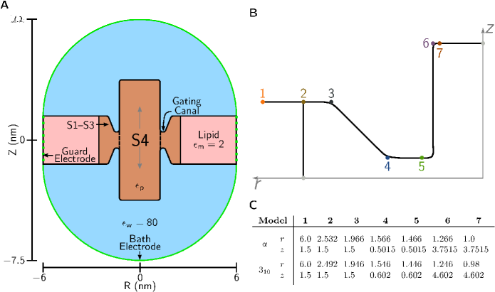
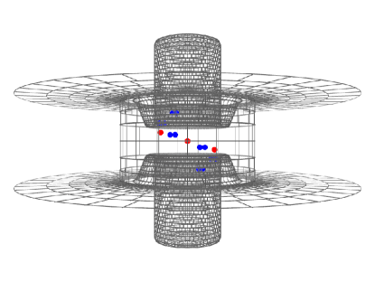
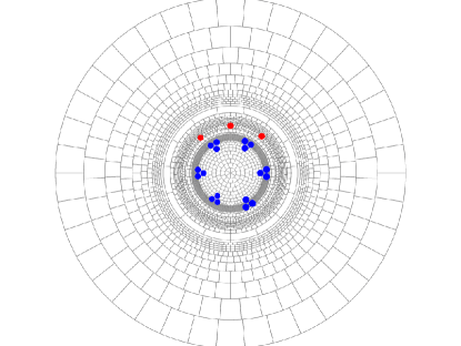
Point source charges representing protein charges are arranged at a minimal distance of nm from the protein/water boundary. The charged guanido group of each arginine residue of the S4 segment is represented as three point source charges of on a circle of radius nm [blue (dark gray) spheres in Fig. 2]. The centers of the S4 arginine charges are arranged on a helix defined by arginine side chains on an - or helix backbone, where every third amino acid is an arginine. For the helix, charged residues are separated by nm in the transmembrane direction and 60∘ leftward around the helix; for the helix, charged residues are separated by nm and ∘.
Dimensions of the simulation surfaces are varied within those constraints as defined in Figs. 1(B) and 1(C). Figure 1(B) maps the topology of the protein and membrane surface of Fig. 1(A) onto metrics for simulations, defined in Fig. 1(C). Since the surfaces in the system are radially symmetrical and smooth, the system is defined by a set of inflection points with their curvature on the left half of the system to be simulated. Since the gating canal is symmetrical in these models, this further reduces to the upper half of the left side.
We analyze two degrees of freedom for the movement of the S4 segment: the curve on which (triplets of) S4 charge centers are aligned can be both translated along the helix axis and rotated about that axis. The model S4 charges thus move like parts of a solid body. Negatively charged residues contributed by the S2 and S3 transmembrane segments of the natural VS are modeled as point source charges of fixed on a curve parallel to the curve on which S4 charges are centered [red (light gray) spheres in Fig. 2]; the offset from the helix axis of the countercharge curve is nm larger than the radius of the curve of the centers of the (triplets of) S4 charges [see Fig. 1(C)]. The axial and angular intervals between countercharges are discussed in Sec. IV. countercharges are stationary in their assigned positions.
The electrodes encapsulating the simulation cell serve three purposes:
-
1.
The bath electrodes provide Dirichlet boundary conditions corresponding to a voltage clamp.
-
2.
The bath electrodes substitute for screening by bath ions of uncompensated protein charge. Screening by the ions in an aqueous bath is equivalent to the screening provided by charge on a metal foil placed in the water a distance away from the protein boundary. In the Debye-Hückel theory, an electrode distance of nm corresponds to the physiological bath ionic strength; thus the electrode location shown in Fig. 1(A) corresponds to a bath solution in the low millimolar range. An alternate configuration, a simulation cell with the bath regions omitted and the electrodes placed directly on the membrane and protein boundaries, would establish screening at the Onsager limit approached at exceedingly large ionic strength. In this way, the possible range of screening effects can in principle be determined without including explicit bath ions in the simulation.
-
3.
At the surface where the membrane region meets the cell boundary, a set of guard electrodes forming rings around the cell maintain a graded far potential varying, from ring to ring, between the potentials applied at the inner and outer bath electrodes. These guard electrodes impose at the membrane edge a far potential similar to that existing in a macroscopic system.
Translational and rotational motions of the S4 helix are simulated by allowing the ensemble of S4 charges to slide within the dielectric domain of the protein shown in Fig. 1. The protein dielectric itself does not slide with the charges. With the protein dielectric extended far enough into the baths, keeping the S4 dielectric stationary has negligible electrostatic consequences because the dielectric of the model is uniform within the protein domain. Simulating S4 motion in this way reduces the computational effort of model exploration by several orders of magnitude.
III Methods
III.1 Electrostatics
We are concerned with the electrostatic interactions among charged groups of the VS protein, electrode charges and charges induced on sharp dielectric boundaries. In solving the electrostatics, we take advantage of the fact that all other charges besides the point source charges of the protein are distributed on a few boundary surfaces rather than distributed throughout a volume. The primary task of calculating electrostatic interactions consists in determining the charge distributions on the electrode and dielectric boundaries, distributions which are initially unknown for a given configuration of protein charges and applied voltage.
III.1.1 Computation of unknown charges
Boda et al. (2006) have described and tested a boundary element method (the induced charge calculation) for computing the charge distribution on the dielectric boundaries of a system consisting of point source charges and linear isotropic dielectrics with sharp boundaries. We include an additional electrostatic element, the ‘electrode’: an infinitesimally thin conductive foil charged to a prescribed electric potential using an external source. In our system, this surface is also a dielectric boundary between the simulation cell and the dielectric surrounding the cell (e.g., vacuum). Thus the charge of an electrode is in part induced charge (as in the paper by Boda et al.) and source charge (to fix the prescribed potential). In the following, we show how the total electrode charge can be calculated without needing to separately calculate its parts. The electrode charge calculation complements the induced charge calculation, making it possible to calculate all the initially unknown charges in the system.
The spatial density of source charge in our system is composed of the point source charges of the VS protein located at positions and source charge distributed on the electrodes with surface density .
The polarization charge density induced at any location in a dielectric is
| (1) |
where is the generally location-dependent dielectric coefficient, the permittivity of the vacuum, and the electric field strength produced by all (source and induced) charges in the system. This relation follows from Poisson’s equation (including polarization) and the constitutive relation describing polarization in a linear, isotropic dielectric (Boda et al., 2006). The first term on the right-hand side of Eq. (1) describes the charge induced on the surfaces of the volume element at if the element contains source charge. The second term describes charge induced in the volume element by the electric field if the dielectric coefficient at has a non-zero gradient.
For our charge calculations, we combine collocated source and induced charges into an effective charge for computing the field and potential. The effective charge density associated with a known source charge density embedded in a dielectric [described by a locally uniform ] is
| (2) |
The effective charge density of an electrode includes both contributions to the induced charge described by Eq. (1), as well as the source charge.
The dielectric boundaries inside the simulation cell (marked in heavy black in Fig. 1; all lines but the electrodes) do not carry source charge. However, the electric field in the simulation cell induces the charge density at locations . This induced charge density is initially unknown.
The field strength and potential in our system are produced by the superposition of the fields and potentials of the source and induced charges:
| (3) |
| (4) |
where is the area of the surface element at location .
The unknown induced surface charge density on the dielectric boundary is related to the field strength by (Boda et al., 2006)
| (5) |
where is any location on the surface , is the difference in the dielectric coefficient across the dielectric boundary in the normal direction , and is the mean of the dielectric coefficients at the boundary location.
The potential at any location on the electrode surfaces has a value imposed by the voltage clamp:
| (6) |
Inserting the expression for the electric field strength from Eq. (3) into Eq. (5) and inserting the expression for the electric potential from Eq. (4) into Eq. (6) yields two integral equations in terms of both and . The initially unknown charge densities on the dielectric and electrode boundaries are the joint solution of these two integral equations.
To solve the integral equations, we follow the method of Boda et al. (2006). The surfaces and are subdivided into curved surface elements. The unknown charge densities are approximated as uniform on each surface element. The two integral equations then become one system of linear equations in terms of the unknown charge densities of a finite number of surface elements.
The inhomogeneity of surface charge in our simulation is greatest where point source charges of the VS protein are close to a dielectric boundary or electrode. For computational efficiency, we vary the size of the surface subdivisions depending on the distance from the point source charges. A typical surface grid (comprising 7000 surface elements) is shown in Fig. 2 for the dielectric surfaces in the simulation cell. The electrode surfaces (not included in Fig. 2) are subdivided into 1700 relatively large elements because of their distance from point source charges.
The computation of the unknown charges on the surface elements involves solving a linear equation system in terms of as many unknowns as there are surface elements. The coefficient matrix of this system is dense, therefore the LU-decomposition time increases with . This computational disadvantage is greatly alleviated by the fact that -decomposition of the coefficient matrix needs to be done only once for a given combination of surface geometry and dielectric coefficients. When the S4 charges are moved, solutions to this system of equations are obtained by back-substitution using the same LU-decomposed matrix. That operation (back-substitution) is required for each sampled configuration of VS charges but not for each applied voltage tested, as described later.
Accuracy of charge calculation.
The divergence theorem (Gauss’s theorem) states that
| (7) |
where is the closed surface around the volume , is the area of the surface element located at , is the normal unit vector for that surface element, is the volume of the space element located at , and is the source charge density inside the volume.
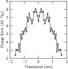
Gauss’s theorem provides a sum-rule test for our solution of the electrostatics that is applicable to the specific geometry used in a simulation. We verify the theorem at the dielectric boundary of the VS protein because: 1) that boundary is closest to the protein source charges of interest; and 2) the field at that boundary produces the largest density of induced charge in our system. The volume integral in Eq. (7) yields the known algebraic sum of the point source charges assigned to the VS residues. The surface integral can be expressed in terms of the charges induced by the normal field at the discretized dielectric boundary. We consider the residue given by the difference of the surface and volume integrals as a measure of our numerical error:
| (8) |
where is the area of the protein surface element , the dielectric coefficient on the out-facing side of , and the induced charge density computed to solve the electrostatics.
The error in the induced charge calculation is likely to vary as S4 charges are moved in a simulation since the distances between the S4 charges and the dielectric boundary vary. Figure 3 shows the error in induced charge calculation for the full range of S4 translational positions sampled in a typical simulation. The error is of the actual net charge of assigned to the VS in this simulation. The results of our charge calculation are thus in good agreement with Gauss’s theorem, as they must be. This test was performed for every simulation.
III.1.2 Computation of charge displacement and electrostatic energy
When the charges of the VS change position, the electric flux toward one bath electrode generally increases by the same amount as the electric flux decreases toward the other bath electrode. To maintain a constant voltage between the two electrodes, charge has to be moved externally between the electrodes. This charge is the experimentally measured displaced gating charge. In principle, one can measure displaced charge in a simulation by monitoring electric flux across a surface surrounding a bath electrode. A more efficient method is provided by the Ramo-Shockley (RS) theorem (Shockley, 1938; Ramo, 1939); for an application to ion channels see (Nonner et al., 2004)). The RS theorem lays the groundwork as well for an efficient method of computing the electrostatic energy of VS configurations when the applied voltage is varied (He, 2001). The RS theorem is applicable to systems containing linear dielectrics.
The RS theorem can be formulated for the configuration of electrode potentials in this study. We apply equal and opposite potentials and to the internal and external bath electrodes to create a membrane voltage (defined as internal minus external potential). We determine the displaced charge in a simulation in two steps:
-
1.
Set all point source charges to zero and apply V at the internal and V at the external bath electrode. Solve for the unknown electrode and induced boundary charges. From these charges, an electric potential can be computed for any geometrical location of the simulation cell.
-
2.
In a simulation with the actual point source charges present and arbitrary potentials and applied at the internal and external bath electrodes, determine the displaced charge from the relation
(9) Note that for all geometrical positions where , and varies between and as the position of is varied from the internal to the external bath electrode.
When several point source charges are in the simulation, the total displaced charge is the algebraic sum of the displaced charges defined by Eq. (9) for each point source charge:
(10)
Step 1 is executed once for the chosen configuration of electrodes and dielectrics in the simulation (including dielectric coefficients). Step 2 is executed once for each configuration of point source charges. Since the displaced charge determined in step 2 is invariant with respect to the potentials applied at the electrodes, it needs to be calculated only once for each point-charge configuration, regardless of variation in the electrode potentials.
The RS theorem also makes it possible to compute the electrostatic energy of a VS configuration with the algebraic sum of two terms:
| (11) |
determined by separate calculations:
-
1.
In a simulation which includes the point source charges at positions , impose the potential on all electrodes and compute the self-energy
(12) where is determined by Eq. (4), excluding self-interactions for each source charge .
-
2.
Calculate the displaced charge corresponding to the point source charges and their positions using Eq. (10). For the imposed voltage , calculate:
(13)
Step 1 of this procedure is executed once for each sampled configuration of point source charges. Step 2 is executed repeatedly for each applied voltage that is tested.
The calculations of displaced charge and electrostatic energy via Eqs. (10) and (11) are independently verified by computing the electrostatic energy by the path integral of the electric force acting on the charges of the VS as those charges move from to :
| (14) |
Here, the electric field is the field of all charges in the system except the charge itself, as defined by Eq. (3).
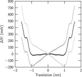
Figure 4 shows this control for three different applied voltages over a prescribed (diagonal) path through the translational and rotational dimensions of the range of S4 motion typically sampled by us. There is good agreement between the energies computed using the Ramo-Shockley theorem (dots) or through the path integral of force (lines).
III.2 Statistical mechanics
Displaced gating charge is experimentally measured from ensembles of channels and thus is an ensemble average. Our electrostatic calculations yield both the displaced charge and the electrostatic part of the configurational energy for a given configuration of a simulated VS model. We consider whole-body movements of S4 charge in two degrees of freedom: translation along the S4 axis and rotation about that axis. Our computational method is efficient enough to allow systematic sampling of this configuration space. We represent each dimension by 51 equally spaced grid nodes and compute the electrostatic energy for the 2601 nodes of the two-dimensional space.
The energy samples define a canonical partition function describing the consequences of the electrostatics on the distribution of an ensemble in the discretized configuration space:
| (15) |
where and are the indices of the rotational and translational discrete positions; is the electrostatic configurational energy of the voltage sensor at translational position and rotational position ; is the Boltzmann constant; and K is the absolute temperature. The sampled rotational range is ∘, and a typical translational range is nm to nm relative to the central position of the S4 charges in -helical models ( nm for -helical models). Restricting the configuration space this way is equivalent to including hard-wall potentials into the Hamiltonian [Eq. (11)].
The probability of a VS configuration for a particular translation and rotation is
| (16) |
and the expectation (mean) value of a random variable is
| (17) |
We also determine the expectations of random variables over the rotational degree of freedom for a particular translational position :
| (18) |
The goal of our simulations is to study the energetics of the movement of the S4 segment for two degrees of freedom. We are concerned only with variation of the Hamiltonian due to changes in S4 position for this space. Since these simulations are done for varied settings of an external parameter (applied voltage), the energy at the reference position for must be invariant with respect to applied voltage.
In our simulations, a voltage is applied across the bath electrodes by imposing the potentials and at the internal and external bath electrodes. Hence, there are locations in the simulation cell where the potential due to the applied field and the displaced charge for any point charge there are zero for any [Eq. (9)]. Since we are concerned with the position of the S4 segment which bears point charges at several locations, we define the S4 reference position such that the total displaced charge there is zero. By Eq. (10) and due to the polarity of the fields applied, there are positions for the S4 segment where is zero, and therefore the energy for those configurations is invariant with regard to . Because of the symmetries in this study, these reference positions coincide with the origin of the translational axis ( nm for any rotation ; we choose ).
III.3 Online Supplemental Materials
Figures 9 & 10 and the associated Supplemental Animations 1 pey (a) & 2 pey (b) illustrate VS geometry and movement for the simulations presented in this paper. They show the expectation(s) of position for VS charges superimposed over the distribution of charge density. In the animation, voltage is changed in a ramp from to mV. Note that these animations are of the VS without an external load attached — as in Sec. IV.1 rather than Sec. IV.2.
IV Results and Discussion
The relationship between the expectation of displaced charge and the applied membrane voltage in a sliding-helix model of an individual VS domain is shown in Fig. 5(A). The solid line represents the computed relation. Open circles represent the relationship experimentally observed in ShakerB K+ channels (Fig. 2A in Seoh et al., 1996) — the experimental charge per channel was divided by the number of channel monomers (4, where each includes one VS domain). Three observations can be made by comparing the two relations: (1) the total amounts of charge that can be moved by large changes of voltage are similar, elementary charges per VS domain; (2) the slopes of the two relations are similar; and (3) a shift along the voltage axis is needed to align the midpoint of the computed relation with the midpoint of the experimental relation (dashed line).
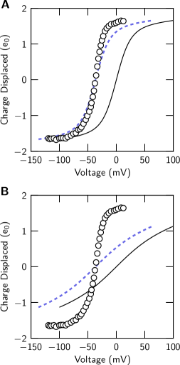
The VS charges in the simulation for Fig. 5(A) are arranged according to an -helical geometry (Figs. 2 & 9). An analogous simulation in which the VS charges conform to a -helical geometry (Fig. 10) yields a different result [Fig. 5(B)]. With regard to the experimental charge-voltage relation, the model yields less total charge movement over the tested voltage range and a smaller maximal slope.
The models giving the charge-voltage relations of Fig. 5 involve idealized domain geometries and use the dielectric coefficient . These are initial choices made in this study — no variations were made to produce more realistic predictions. The geometries of S4 charges were idealized to conform with two kinds of helices. The countercharges () were arranged on a spiral ( helix) or straight line ( helix) paralleling the curve of the S4 charges. The only parameter optimized in light of the experimental results was the countercharge spacing (the translational and angular intervals between countercharges). In the models used in this paper, countercharges are spaced at the intervals of the S4 charges, so that at most one S4 charge lines up with a countercharge for any particular S4 position.
The simulations reported in Fig. 5 indicate that voltage sensing by a sliding-helix is robust from an engineering point of view. In these generic models, either the - or -helical S4 structure can produce voltage-dependent charge displacement, even though the two structures involve distinct configurations of the protein charges. The two forms of helix generate different responses to voltage in the tested models, but neither form produces catastrophic failure. The biological channels whose structure-function relation we seek to ultimately understand in engineering terms themselves show robustness: different channel types exhibit a wide range of response to voltage while remaining functional under many mutations that cause their response to change, and yet they all use a common architecture. On these grounds, useful insights are expected from analyzing a mesoscale physical model.
IV.1 Energetics of ‘idling’ voltage sensors
The mobile charges of the VS model lie within the electric field of the charges on the electrodes, the stationary countercharges, and the charges induced in the dielectrics. We model those mobile charges as parts of a solid body with two degrees of freedom of solid-body motion: translation along the S4 axis and rotation about that axis. Energy is computed on a grid over this configuration space [Eq. (11)]. From the electrostatic energy map, a partition function is constructed [Eq. (15)], and from the partition function, statistics of random variables [Eq. (17)] are predicted. The energy map thus defines the expectations of observables such as the gating charge displacement (Fig. 5). This energy map is computed for each tested value of applied voltage. These maps and the resulting partition functions are outputs of the model system.
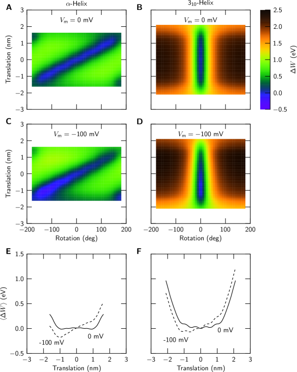
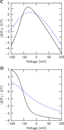
Pseudo-color maps of electrostatic energy in the two dimensions computed for applied voltages of mV and mV are shown in Fig. 6. The translational and rotational origins correspond to the central S4 position shown in Fig. 2 for the helix (change in energy is relative to those origins, where is zero). Because of the symmetry of these models, the map for mV (not shown) is a mirror image of the map for mV.
For a membrane voltage of mV, the energy maps of both helical models reveal a trough bounded on all sides by regions of substantially higher energy. The energy trough runs in the direction of proportional translation and rotation for the -helical S4 model, but it runs in the direction of simple translation for the -helical S4 model. The trough in the map of each model follows the countercharge arrangement — an arrangement chosen for each model to allow periodic interactions during S4 motion of the S4 charges with the countercharges. In the -helical model, the S4 charges and countercharges are aligned on parallel super-helices, whereas in the -helical model the S4 charges and countercharges follow straight lines parallel to the helical axis. The lowest electrostatic energies of the -helical S4 segment trace the path of a screw, whereas the energies of the -helical S4 segment trace the path of a piston.
The regions outside the energy trough for the helix have energies about three times as large as those of the helix. The electrostatic confinement of the helix is stronger than that of the helix. The strength of confinement correlates inversely with the separation of charges in the two geometries. The cluster of S4 charges and countercharges is more spread out in space in the -helical than in the -helical geometry due to the angular separations of charges in the -helical S4 segment.
The electrostatic energy trough tends to anchor the sliding-helix in a transmembrane configuration. The S4 charges that, for a given configuration, dwell in the region of small polarizability are balanced in this model by countercharges located in that region. This balance is maintained over the range of S4 travel where equivalent amounts of S4 charge and countercharge overlap in the region of weak dielectric (see the Supplemental Material, animation 1 pey (a) & Fig. 9 below). A second essential element of balance concerns the transit of S4 charges between the less polarizable gating canal region and the more polarizable vestibule and bath regions. Any energy change associated with the transit of an S4 charge on one side is approximately balanced on the other side by the opposite transit of an S4 charge. On the other hand, the energy trough generated by the electrostatics of the models is too shallow by itself to ensure long-term stability of the S4 configuration. Interactions beyond those included in the model (such as linkages to adjacent transmembrane segments or hydrophobic effect of the uncharged S4 residues) are necessary for long-term stability.
To inspect the energetics more closely, we construct a one-dimensional energy profile for S4 translation by computing for each translational position the expectation of the electrostatic energy in the rotational degree of freedom using the rotational partition function [Eq. (18)]. We refer to this kind of energy profile as a ‘translational energy profile’ for short. Figures 6(E) & 6(F) show the translational energy profiles for two applied voltages: mV (solid lines) and mV (dashed lines). The profiles at mV are quite uniform over the translational extent of the energy trough (a consequence of the chosen spacing of countercharges). At a membrane voltage of mV, the energy profiles are tilted in favor of more intracellular positions. A well-defined energy minimum is found at a position about nm inward from the central position of the -helical S4 segment, whereas a broad minimum spread between and nm is found with the -helical S4 segment.

The energy profiles in Fig. 6 do not resemble the profile of an ion embedded in a lipid membrane — the latter profile has a high barrier in the center of the weak dielectric (Parsegian, 1969; Neumcke and Läuger, 1969). Instead, in these models the charged section of the S4 helix can travel with an almost level energy over the translation range where S4 charges overlap with stationary countercharges. To examine the contribution of the countercharges to this result, we re-compute the energy profile for the -helical S4 segment with the countercharges deleted from the model (Fig. 7). Deletion of the countercharges converts the energy trough seen with the standard model (dashed line) into a broad barrier (solid line). That barrier is reduced but not inverted by increasing the VS dielectric coefficient from to (dotted line). For comparison, a sliding-helix model without countercharges using has been analyzed previously by Grabe et al. (2004).
Over the range of translation where the countercharges produce an energy trough (dashed line), the deletion of the countercharges (solid line) has a rather small effect (note that we plot energy relative to the central position). Movement of the S4 helix encounters little energy variation in this region of translation because the amount of S4 charge present in the domain of weak dielectric does not vary: as S4 charge enters on one side, S4 charge leaves on the other side. The energetics are not favorable for these S4 positions (as the charges are not balanced), but they are rather uniformly unfavorable until S4 translation exceeds 1 nm from its center position. If the travel of the S4 helix is restricted to nm in a biological channel by means other than the countercharges deleted here, then even an S4 segment without balancing countercharges could perform as a voltage sensor.
The variations of energy are small over the traveled range of translation in Figs. 6(E) & 6(F). The restriction in the model that the S4 domain and its charges must move as a single solid body might be expected to ‘synchronize’ periodic interactions among charges and countercharges, leading the energetics to express several distinct barriers and wells. The chosen spacing of the countercharges, however, is enough to prevent the emergence of such a pattern. Additional degrees of freedom are thus not a prerequisite for smooth S4 travel (examples of such degrees of freedom are the possible flexibility of the individual charge-bearing S4 residues or changes in configuration of the helix between the and forms, Long et al., 2007; Khalili-Araghi et al., 2010; Bjelkmar et al., 2009; Schwaiger et al., 2011).
Although the energy profiles of the two helix forms are similar, the small differences between them are sufficient to produce substantial differences in the relations between displaced charge and voltage (Fig. 5). Because of the small size of these energy differences, contributions to the Hamiltonian not included in the model (in particular contributions arising by coupling of the VS to other parts of the channel) could override the differences between the S4 helix versions seen in Fig. 5 and Figs. 6(E) & 6(F).
Additional axes of variation for these models with consequences for voltage gating include the geometry of the gating pore region, the dielectric coefficient of the protein region, the distribution of countercharges, and the effects of additional surface charges. We have partially explored these spaces (Peyser and Nonner, 2011). The robustness of the mechanism explored here in the face of pathology due to mutation can also be explored with this approach, given the computational tractability of these mesoscale models.
IV.2 Energetics of ‘working’ voltage sensors
The essence of a voltage sensor is that it can do external work when the membrane voltage is varied. This work can then be applied, for instance, to reconfiguring the channel between conducting and non-conducting configurations (gating). In order to determine the work that a voltage sensor model might produce, we simulate models with a translation-dependent external workload included in the Hamiltonian. The potential energy field in which the S4 domain translates and/or rotates then comprises the electrostatic potential energy described by Eq. (11) plus the potential energy due to the load:
| (19) |
For our examples, we use a hypothetical load field producing a constant force opposing the inward translation of the S4 segment and hence a load potential that varies linearly with translation [Fig. 8(A)]. This describes the energetics if, for instance, the gate of a hypothetical channel with a single VS resists closing (by inward movement of the S4 helix) with a constant force.
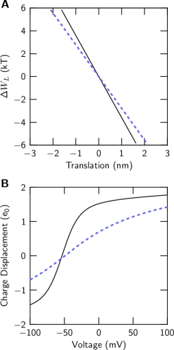
The presence of this load alters the relation between the mean displaced charge and voltage by shifting the curve to negative voltages [Fig. 8(B), compare Fig. 5]. In the case of the -helical S4 model, the charge-voltage curve becomes quite similar to that observed in the experiment with full channels [symbols in Fig. 5(A)].
In order to assess the relationship between the electrical work picked up by the VS and the external work delivered to the load, we consider the expectations of [Fig. 8(C)] and [Fig. 8(D)]. The expectation for has a simple relationship to the expectation of displaced charge:
| (20) |
The work exchanged between the VS and the load () varies most strongly with voltage where the variation of displaced charge is maximal, as expected if the load depends on S4 position. Two points on the axis of applied voltage are associated with polarity changes of displaced charge and/or of components of the Hamiltonian in Fig. 8 (not marked): for (B), (C), and (D); and for (C). In the voltage region , the applied voltage drives the S4 helix inward while external work is done against the load. In the region , both the applied voltage and the work done on the S4 helix by the load drive the S4 helix outward (). In the intermediate region , the S4 helix is also driven outward (). Here the applied-voltage and load components of the Hamiltonian have opposite polarities: outward S4 motion prevails because the load prevails over the opposing effect of applied voltage.
The translation range traveled by the S4 helix is limited in these simulations by the electrostatics of the VS rather than by the hypothesized load. The limits are set by the electrostatic self-energy component of the Hamiltonian, (Fig. 6, ). Therefore, the work that the VS can do on the load at large (positive or negative) voltages saturates [Fig. 8(D)], whereas the (negative) energy contributed to the VS by the applied field continues to increase in magnitude [Fig. 8(C)]. Biological K+ channels open with very low probability () at large negative voltages with no indication of a saturating minimal probability (Seoh et al., 1996; Schoppa et al., 1992; Aggarwal and MacKinnon, 1996). This may indicate that the load imposed on the VS domains by the ‘gate’ of the channel actually limits S4 travel at large negative voltages. In contrast, at large positive voltages the open probability of the channels saturates at levels well below , suggesting a saturating amount of work that the VS domains can do on the gate.
Figure 8 shows the simulation results for both the and configurations of the S4 helix. The differences in voltage responsiveness observed in the simulations with the idling sensors are also found under the hypothetical load that we test. This observation, however, cannot be generalized. The differences between these two forms of VS result from the associated electrostatic self-energies (as seen in Fig. 6). In the Hamiltonian of the system under load [Eq. (19)], characteristics are determined by the sum of the self-energy term and the load term . Hence, it is in principle possible that the load transforms the characteristics of voltage sensing observed here for the -helical VS model into characteristics indistinguishable from those of the -helical VS model or vice-versa, or a load may even result in behaviors different from those seen in either simulation. Experimental observations on displaced charge therefore cannot be interpreted in terms of models that include only a voltage sensor. These observations, like those on gating, require a model of the full channel to be analyzed.
The mesoscale model system that we have presented for a single VS is extendable using the approach described in this section. The Hamiltonian of the system can be extended by terms describing the energetics of a channel comprising four voltage sensors, a gating domain, and their coupling. The number of degrees of freedom (e.g., two for each voltage sensor) remains computationally manageable, so that a mesoscale model of the full channel can be simulated in order to obtain insight into the cooperation of its parts.
We have analyzed here some equilibrium properties of a VS domain in which the S4 helix is relocated as a solid body. A refined model augmented with dynamics will likely have to include a second scale describing motions of side chains, possible deformations of the S4 helix, interactions with the bath solutions, and associated dissipative aspects. General energetic variational approaches developed for hydrodynamic systems of complex fluids (Hyon et al., 2010) may provide a multi-scale approach to channel dynamics.
Acknowledgements.
The authors are grateful for the support of the National Institutes of Health (Grant No. GM083161) to W.N. and a Graduate Research Fellowship of the National Science Foundation to A.P. We thank Dr. Alice Holohean, Dr. Peter Larsson, and Dr. Karl Magleby for helpful discussions.*
Appendix A Charge distributions of VS models
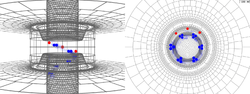
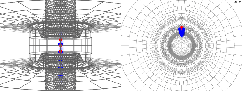
The sliding helix in our VS models is a microscopic voltage sensor. Therefore, we describe the VS by its statistical ensemble behavior. In this appendix, stochastic VS behavior is visualized for several models presented in the paper, both as figures for a fixed applied voltage ( mV; Figs. 9 & 10) and as associated Supplemental Materials, animations 1 pey (a) & 2 pey (b) with voltage increasing uniformly over time from mV to mV.
The figures show two stochastic aspects of VS behavior: (1) the mean positions of the S4 charges [marked by blue (dark gray) balls], and (2) the charge density distribution of S4 charge [represented by a blue (gray) cloud with a color intensity proportional to the charge density there]. A high density of color marks the locations where the S4 charges dwell frequently, as opposed to their mean positions.
The expectation of position for each charge is computed from Eq. (17) using the positions for the charge as the random variable , over the partition function with translational and rotational degrees of freedom. Since the helix behaves as a solid body, the helix position fixes the positions for the charges . That relationship allows us to define the partition function, the energy function, the configuration probability and our measures for the positions in terms of the respective function for the helix position . For the expectation of position for each charge:
| (21) |
where is the work needed to construct configuration , is the probability of that configuration, and is the position of charge in configuration .
Likewise, the distribution of charge can be computed by applying the partition and energy functions in terms of the positions of charges . The charge density is then the sum over all charges of the probability of each charge being located at , multiplied by its valency in units of , and normalized:
| (22) |
where is the discretized delta function ( if we are treating as the same location as for visualization purposes; otherwise ).
The color representations for the animations are proportional to , normalized to the highest charge density at that frame’s potential.
References
- Hodgkin and Huxley (1952) A. Hodgkin and A. Huxley, J Physiol 117, 500 (1952).
- Hille (2001) B. Hille, Ion Channels of Excitable Membranes, 3rd ed. (Sinauer Associates, Inc., Sunderland, Mass. USA, 2001).
- Gandhi and Isacoff (2002) C. S. Gandhi and E. Y. Isacoff, J Gen Physiol 120, 455 (2002).
- Catterall (2010) W. A. Catterall, Neuron 67, 915 (2010).
- Gonzalez et al. (2012) C. Gonzalez, G. Contreras, A. Peyser, P. Larsson, A. Neely, and R. Latorre, Biophys Rev 4, 1 (2012).
- Catterall (1986) W. Catterall, Annu Rev Biochem 55, 953 (1986).
- Berry et al. (2000) R. S. Berry, S. A. Rice, and J. Ross, eds., Physical Chemistry, 2nd ed., Topics in Physical Chemistry (Oxford University Press, 2000).
- Schoppa et al. (1992) N. E. Schoppa, K. McCormack, M. A. Tanouye, and F. J. Sigworth, Science 255, 1712 (1992).
- Seoh et al. (1996) S.-A. Seoh, D. Sigg, D. M. Papazian, and F. Bezanilla, Neuron 16, 1159 (1996).
- Aggarwal and MacKinnon (1996) S. K. Aggarwal and R. MacKinnon, Neuron 16 (1996).
- Papazian et al. (1995) D. M. Papazian, X. M. Shao, S. A. Seoh, A. F. Mock, Y. Huang, and D. H. Wainstock, Neuron 14, 1293 (1995).
- Lecar et al. (2003) H. Lecar, H. P. Larsson, and M. Grabe, Biophys J 85, 2854 (2003).
- Grabe et al. (2004) M. Grabe, H. Lecar, Y. N. Jan, and L. Y. Jan, Proc Natl Acad Sci U S A 101, 17640 (2004).
- Silva et al. (2009) J. R. Silva, H. Pan, D. Wu, A. Nekouzadeh, K. F. Decker, J. Cui, N. A. Baker, D. Sept, and Y. Rudy, Proc Natl Acad Sci U S A 106, 11102 (2009).
- Hodgkin et al. (1952) A. Hodgkin, A. Huxley, and B. Katz, J Physiol 116, 424 (1952).
- Armstrong and Bezanilla (1973) C. Armstrong and F. Bezanilla, Nature 242, 459 (1973).
- Long et al. (2007) S. B. Long, X. Tao, E. B. Campbell, and R. MacKinnon, Nature 450, 376 (2007).
- Khalili-Araghi et al. (2010) F. Khalili-Araghi, V. Jogini, V. Yarov-Yarovoy, E. Tajkhorshid, B. Roux, and K. Schulten, Biophys J 98, 2189 (2010).
- Bjelkmar et al. (2009) P. Bjelkmar, P. S. Niemelä, I. Vattulainen, and E. Lindahl, PLoS Comput Biol 5, e1000289 (2009).
- Schwaiger et al. (2011) C. S. Schwaiger, P. Bjelkmar, B. Hess, and E. Lindahl, Biophys J 100, 1446 (2011).
- Boda et al. (2006) D. Boda, M. Valiskó, B. Eisenberg, W. Nonner, D. Henderson, and D. Gillespie, J Chem Phys 125, 34901 (2006).
- Shockley (1938) W. Shockley, J Appl Phys 9, 635 (1938).
- Ramo (1939) S. Ramo, Proc IRE 27, 584 (1939).
- Nonner et al. (2004) W. Nonner, A. Peyser, D. Gillespie, and B. Eisenberg, Biophys J 87, 3716 (2004).
- He (2001) Z. He, Nucl Instr Meth A 463, 250 (2001).
- pey (a) See Supplemental Material file alpha-helix.mpg in the Data Conservency data set associated with http://arxiv.org/abs/1203.6061 for Supplemental Animation 1 associated with Fig. 9 which illustrates the VS geometry, movement and charge density distribute over the range of mV to mv for the standard -helical model presented in this paper.
- pey (b) See Supplemental Material 3-10-helix.mpg in the Data Conservency data set associated with http://arxiv.org/abs/1203.6061 for Supplemental Animation 2 associated with Fig. 10 which illustrates the VS geometry, movement and charge density distribution for the standard -helical model presented in this paper.
- Parsegian (1969) A. Parsegian, Nature 221, 844 (1969).
- Neumcke and Läuger (1969) B. Neumcke and P. Läuger, Biophys J 9, 1160 (1969).
- Peyser and Nonner (2011) A. Peyser and W. Nonner, (2011), arXiv:1112.2994v1.
- Hyon et al. (2010) Y. Hyon, D. Kwak, and C. Liu, Discret Contin Dyn S A 26, 1291 (2010).