Suppression of low-frequency noise in two-dimensional electron gas at degenerately doped Si:P layers
Abstract
We report low-frequency noise measurements of degenerately doped Si:P -layers at K. The noise was found to be over six orders of magnitude lower than that of bulk Si:P systems in the metallic regime and is one of the lowest values reported for doped semiconductors. The noise was found to be nearly independent of magnetic field at low fields, indicating negligible contribution from universal conductance fluctuations. Instead interaction of electrons with very few active structural two-level systems may explain the observed noise magnitude.
As classical information processing technology approaches the sub-20 nm node, it is becoming increasingly important to control the exact number and position of dopants in electronic devices ITR (2009); Kuhn et al. (2008). Recent progress in using scanning tunneling microscopy (STM) as a lithographic tool allows positioning of dopants with atomic scale precision Schofield et al. (2003). Combined with molecular beam epitaxy, this technology has been employed to realize heavily -doped, planar nanostructures, such as tunnel gaps Rueß et al. (2007a), nanowires Rueß et al. (2007b) and quantum dots Fuhrer et al. (2009); Fuechsle et al. (2010). The same approach can also be used to fabricate vertically-stacked, multiple electrically-active layers McKibbin et al. (2009). The time averaged transport properties of Si:P -doped layers have now been studied in detail Goh et al. (2006); Rueß et al. (2007b); Fuhrer et al. (2009); Fuechsle et al. (2010), but very little is known about its long term charge stability, which reflects in low frequency flicker noise in the electrical transport. The importance of this issue is paramount to the overall development of devices with controlled dopant positioning at the nano-scale and in particular for single dopant spin based qubits Hollenberg et al. (2004).
The noise properties of bulk doped Si has been studied in the metallic regime as well as near the metal-to-insulator transition (MIT). While universal conductance fluctuations (UCF) has been observed in the metallic samples Ghosh and Raychaudhuri (2000), signatures of glassy behavior has been seen near the MIT Kar et al. (2003). The situation is far more unclear when the dopants are confined wihtin one or very few atomic layers. This acquires additional significance due to stronger interaction effects at lower dimensions, theoretical predictions of exotic magnetic states Nielsen and Bhatt (2007); Bhatt and Nielsen (2008) and other possibilities of Hubbard physics close to half filling that are naturally realized in these -doped Si systems.
In this Letter we present the study of low-frequency noise, or -noise, in degenerately doped Si:P -layers. We perform noise measurements as a function of number of carriers to establish that the measured conductivity fluctuations originate from the -layer. We find that the noise is many orders of magnitude lower than bulk doped metallic silicon. Though the magneto-conductivity data indicates weak localization (WL), the magnetic field dependence of noise speaks against any significant contribution from UCF. Instead, interaction of electrons with a small concentration of tunneling two-level-systems (TLS) may explain the extremely low noise in these heavily doped systems.

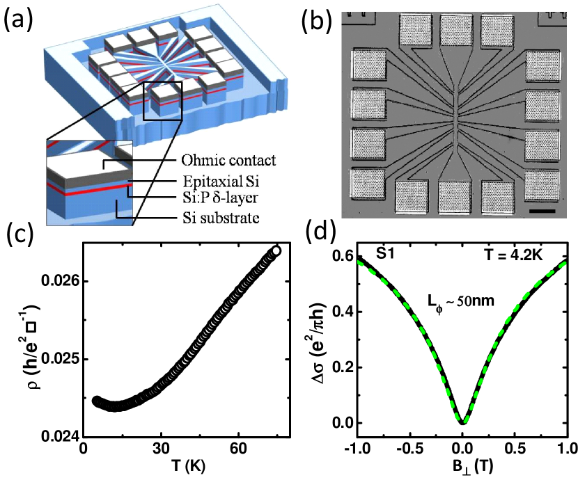
Two Hall bars (S1 and S2) from the same -doped Si:P layer have been studied in this work. The Si:P -layer was fabricated in an ultra-high vacuum variable-temperature STM system equipped with a phosphine (PH3) dosing system and a Si sublimation source. The details of sample fabrication have been reported elsewhere Goh et al. (2006). The trench-isolated Hall bars, were fabricated by electron-beam lithography and reactive ion etching. Figure 1a shows a schematic of the final device structure, wherein a -layer of P atoms is indicated by the red line. Both Hall bars have a width of 20 m and multiple voltage probes for carrier-number dependent noise measurements. Ohmic contacts to the Hall bars were made by depositing 60 nm of nickel (Ni) and 10 nm of titanium (Ti), followed by annealing in nitrogen atmosphere at 350 ∘C and depositing another layer of Ti/gold (Au) (10nm and 60nm respectively). An optical image of the device S2, recorded after deposition of the ohmic contacts, is shown in Figure 1b.

From Hall measurements at temperature K, the two dimensional (2D) electron density of both samples was estimated to be cm-2. Both devices indicate a finite residual resistivity /square, with ( and are Fermi wavevector and mean scattering lengths, respectively). The initial decrease in resistivity with decreasing (from K to 12 K) in both devices (data for S2 not shown) confirms metallic-like behavior(Figure 1c). The upturn in for K is associated with the WL effect. To probe this further, and also extract the phase relaxation length , we have performed four probe magneto-conductance measurement at K. Figure 1d shows the magneto-conductivity plot of S1, measured in a perpendicular magnetic field, () at 4.2K. The dip at is the hallmark of WL behavior. The magneto-conductivity data was fitted with the Hikami formulation Hikami and Nagaoka (1980) for disordered 2D systems, which gives a phase breaking field () of 60mT and 50nm at K. For both resistance and noise measurements, the voltage drop across the device, was kept to minimize heating of electrons.

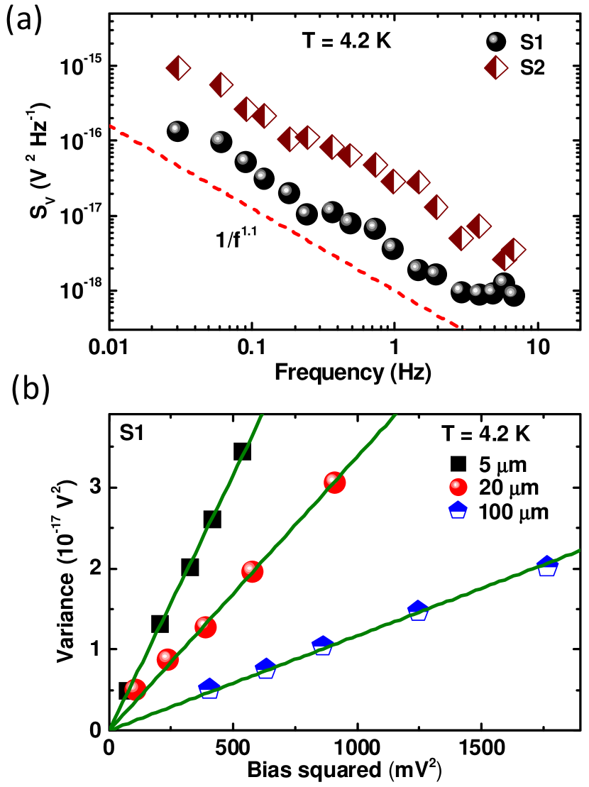
For noise measurements we used an AC four-probe wheatstone bridge technique Scofield (1987); Ghosh et al. (2004); Ghosh and Raychaudhuri (2000). The voltage drop across the sample was amplified by a low noise voltage preamplifier (SR 560) and the output of the amplifier was balanced across a standard wire wound resistor. The voltage fluctuations were recorded as a function of time using a 16 bit digitizer. The raw data was then processed digitally using a three stage decimation process, followed by the power spectral density (PSD) estimation. The details of the noise measurement process can be found elsewhere Scofield (1987); Ghosh et al. (2004). The PSD, (), of noise as a function of frequency is shown in Figure 2a for both the samples. In both devices, we found , where the frequency exponent over the entire experimental bandwidth. The bias dependence of shown in Figure 2b was recorded for different distances between the voltage probes for sample S1. The solid lines show linear fits to the data. was found to be , for all cases, which ensures that we are in the ohmic regime, where the measured voltage fluctuations represent the fluctuations in of the Si:P -layer i.e. . Moreover, the slope of the linear fits decreases as the separation between the voltage probe increases, which essentially means that decreases as the total number of carriers increases.
The frequency and the bias dependence of noise can be combined to normalize the noise magnitude in terms of the phenomenological Hooge relation,
| (1) |
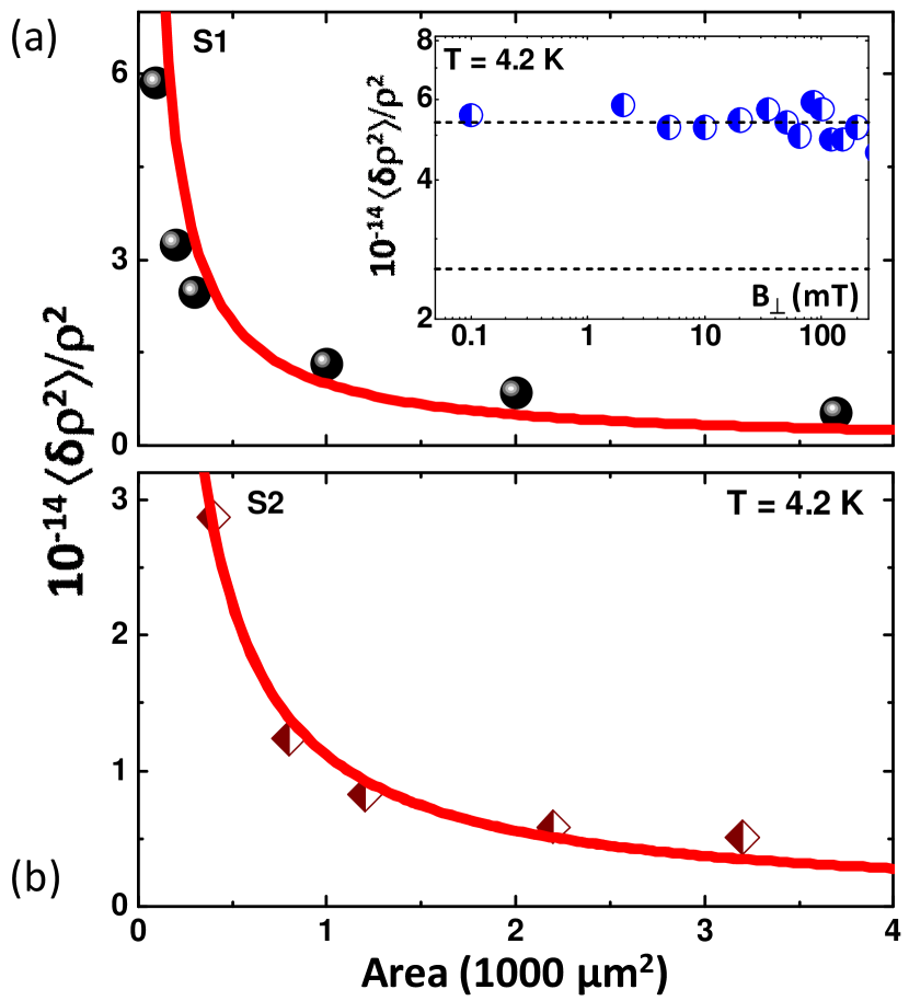
where , and are the phenomenological Hooge parameter, areal density of electrons, and the area of the Hall bar between the voltage probes, respectively. In the data shown in Figure 2, the magnitude of was deduced to be around , which is orders of magnitude lower than that of bulk doped Si:P systems degenerately doped to the metallic regime ( = 0.1-2) Ghosh and Raychaudhuri (1999); Kar and Raychaudhuri (2001). Given such a low value of , it is important to establish that we indeed are measuring the noise from the -layer. Noise measurements were performed for different distances between the voltage probes for both S1 and S2. The results are shown in Figures 3a and 3b, respectively, where / is plotted against the area () of the -layer between the voltage probes (here, ). As expected from the Hooge relation / shows a 1/ dependence, confirming that the measured resistance fluctuations come from the Si:P layer, where different fluctuators contribute independently to the observed noise magnitude.
In order to understand the microscopic origin of noise in Si:P -layers we have investigated the noise magnitude as a function of perpendicular magnetic field () for S1 at T = 4.2K. We find that the remains essentially constant over the range corresponding to the phase breaking field (Inset of Fig. 3a) which is 60 mT at T = 4.2K. The near constancy of noise with shows that universal conductance fluctuations (UCF) as a major source of noise is quite unlikely as we do not see any factor of reduction in McConville and Birge (1993); Ghosh and Raychaudhuri (2000) expected on removal of time reversal symmetry. This is a surprising result since magnetoresistance clearly displays WL (Fig. 1d) and UCF and WL are expected to be manifestations of same quantum interference effect. It is however possible that the low temperature Hamiltonian of our -doped Si system has very different symmetry properties from conventional disordered conductors, although there is no clear understanding of why this should be so.
An alternative possibility is based on a local interference model suggested by Kogan and Nagaev Kogan and Nagaev (1984) with anisotropic scattering of electrons by tunneling TLS. In our system the TLS may be associated with the incorporation of P-atoms in the silicon matrix, as indicated in the bulk-doped systems Ghosh and Raychaudhuri (2000). In this model, the resistivity fluctuations can be expressed as Kogan and Nagaev (1984)
| (2) |
where and are the areal density of the TLS and scattering cross section of the electrons, respectively. Note that in Equation (2) is independent of B. Taking , we estimate . This indicates that the magnitude of the observed noise can be explained if only in million P atoms form active TLS within the experimental bandwidth. Note that charge fluctuations on even a small number of defects can have a spectrum as long as relaxation rates are widely distributed Pellegrini (2000).

It is well known that at extremely high dopant concentrations defects can occur creating deactivating centres either through the formation of donor vacancy clusters, donor pairs or donor pair vacancy interstitials Voyles et al. (2003); Chadi et al. (1997); Mueller and Fichtner (2004); Moon et al. (2008). However using a gaseous dopant source with self limiting absorption of the gaseous dopant precursor it is somewhat surprising that such defect complexes would occur. Other possible explanations could be the incomplete incorporation of dopants into substitutional sites during the incorporation anneal or the potential presence of defects in the epitaxial silicon overgrowth. These results highlight that despite the extremely low noise observed further work is needed to pinpoint exactly what gives rise to the noise floor in these heavily doped devices.
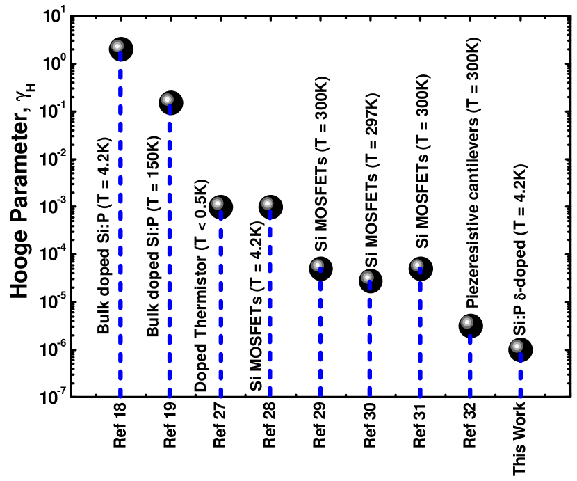
In Fig. 4 we compare the Hooge parameter of our system with the values reported previously for doped Si. Ghosh et. al. Ghosh and Raychaudhuri (1999) and Kar et. al. Kar and Raychaudhuri (2001) have previously measured highly doped bulk Si:P systems and found fairly large values of (0.1 to 2). In comparison to these bulk doped Si:P systems we find that noise in Si:P -layers studied in this work are suppressed by 5 to 6 orders of magnitude. Other references included in Fig. 4 are for doped thermistors McCammon et al. (2002), Si MOSFETs Adkins and Koch (1982); Gaubert et al. (2009); von Haartman et al. (2007); Marin et al. (2004) and piezoresistive cantilevers Yu et al. (2002). An explanation of extreme low noise in our system may involve large elastic energy barriers around the P-atom which immobilizes them and reduces the number of active TLSs. Such barriers may arise during the doping process when the Si-Si bonds distort locally to incorporate the dopants. The remarkably low value of measured here favors the use of Si:P -doped devices as versatile nanoelectronic elements.
In conclusion, we demonstrated suppression of resistance noise in Si:P -layers by several orders of magnitude, in comparison to degenerately doped bulk Si:P systems. The noise is nearly unaffected by low magnetic fields. We indicate the possible role of tunneling two-level systems within a local interference model to understand the microscopic origin of the noise.
We thank Department of Science and Technology (DST), Government of India and Australian-Indian Strategic Research Fund (AISRF) for funding the project. SS thanks CSIR for financial support.
References
- ITR (2009) ITRS Roadmap 2009 edition, available at http://public.itrs.net (2009).
- Kuhn et al. (2008) K. Kuhn, C. Kenyon, A. Kornfeld, M. Liu, A. Maheshwari, W. Shih, S. Sivakumar, G. Taylor, P. VanDerVoorn, and K. Zawadzki, Intel Technology Journal 12, 93 (2008).
- Schofield et al. (2003) S. R. Schofield, N. J. Curson, M. Y. Simmons, F. J. Rueß, T. Hallam, L. Oberbeck, and R. G. Clark, Phys. Rev. Lett. 91, 136104 (2003).
- Rueß et al. (2007a) F. J. Rueß, W. Pok, K. E. J. Goh, A. R. Hamilton, and M. Y. Simmons, Phys. Rev. B 75, 121303 (2007a).
- Rueß et al. (2007b) F. J. Rueß, K. E. J. Goh, M. J. Butcher, T. C. G. Reusch, L. Oberbeck, B. Weber, A. R. Hamilton, and M. Y. Simmons, Nanotechnology 18, 044023 (2007b).
- Fuhrer et al. (2009) A. Fuhrer, M. Fu chsle, T. C. G. Reusch, B. Weber, and M. Y. Simmons, Nano Letters 9, 707 (2009).
- Fuechsle et al. (2010) M. Fuechsle, S. Mahapatra, Z. A., M. Friesen, E. A., and M. Y. Simmons, Nature Nanotechnology 5, 502 (2010).
- McKibbin et al. (2009) S. R. McKibbin, W. R. Clarke, A. Fuhrer, T. C. G. Reusch, and M. Y. Simmons, Applied Physics Letters 95, 233111 (2009).
- Goh et al. (2006) K. E. J. Goh, L. Oberbeck, M. Y. Simmons, A. R. Hamilton, and M. J. Butcher, Phys. Rev. B 73, 035401 (2006).
- Hollenberg et al. (2004) L. C. L. Hollenberg, C. J. Wellard, C. I. Pakes, and A. G. Fowler, Phys. Rev. B 69, 233301 (2004).
- Ghosh and Raychaudhuri (2000) A. Ghosh and A. K. Raychaudhuri, Phys. Rev. Lett. 84, 4681 (2000).
- Kar et al. (2003) S. Kar, A. K. Raychaudhuri, A. Ghosh, H. v. Löhneysen, and G. Weiss, Phys. Rev. Lett. 91, 216603 (2003).
- Nielsen and Bhatt (2007) E. Nielsen and R. N. Bhatt, Phys. Rev. B 76, 161202 (2007).
- Bhatt and Nielsen (2008) R. N. Bhatt and E. Nielsen, International Journal of Modern Physics B 22, 4595 (2008).
- Hikami and Nagaoka (1980) A. I. Hikami, S. Larkin and Y. Nagaoka, Prog. Theor. Phys. 63, 707 (1980).
- Scofield (1987) J. H. Scofield, Rev. Sci. Instrum. 58, 985 (1987).
- Ghosh et al. (2004) A. Ghosh, S. Kar, A. Bid, and A. K. Raychaudhuri, ArXiv Condensed Matter e-prints (2004), eprint arXiv:cond-mat/0402130.
- Ghosh and Raychaudhuri (1999) A. Ghosh and A. K. Raychaudhuri, Journal of Physics: Condensed Matter 11, L457 (1999).
- Kar and Raychaudhuri (2001) S. Kar and A. K. Raychaudhuri, Journal of Physics D: Applied Physics 34, 3197 (2001).
- McConville and Birge (1993) P. McConville and N. O. Birge, Phys. Rev. B 47, 16667 (1993).
- Kogan and Nagaev (1984) S. Kogan and K. Nagaev, Solid State Communications 49, 387 (1984), ISSN 0038-1098.
- Pellegrini (2000) B. Pellegrini, Microelectronics Reliability 40, 1775 (2000).
- Voyles et al. (2003) P. M. Voyles, D. J. Chadi, P. H. Citrin, D. A. Muller, J. L. Grazul, P. A. Northrup, and H.-J. L. Gossmann, Phys. Rev. Lett. 91, 125505 (2003).
- Chadi et al. (1997) D. J. Chadi, P. H. Citrin, C. H. Park, D. L. Adler, M. A. Marcus, and H.-J. Gossmann, Phys. Rev. Lett. 79, 4834 (1997).
- Mueller and Fichtner (2004) D. C. Mueller and W. Fichtner, Phys. Rev. B 70, 245207 (2004).
- Moon et al. (2008) C.-Y. Moon, W.-J. Lee, and K. J. Chang, Nano Letters 8, 3086 (2008).
- McCammon et al. (2002) D. McCammon, M. Galeazzi, D. Liu, W. T. Sanders, P. Tan, K. R. Boyce, R. Brekosky, J. D. Gygax, R. Kelley, D. B. Mott, et al., AIP Conference Proceedings 605, 91 (2002).
- Adkins and Koch (1982) C. J. Adkins and R. H. Koch, Journal of Physics C: Solid State Physics 15, 1829 (1982).
- Gaubert et al. (2009) P. Gaubert, A. Teramoto, W. Cheng, T. Hamada, and T. Ohmi, Journal of Vacuum Science and Technology B 27, 394 (2009).
- von Haartman et al. (2007) M. von Haartman, B. Malm, P.-E. Hellstr m, M. stling, T. Grasby, T. Whall, E. Parker, K. Lyutovich, M. Oehme, and E. Kasper, Solid-State Electronics 51, 771 (2007).
- Marin et al. (2004) M. Marin, Y. A. Allogo, M. de Murcia, P. Llinares, and J. C. Vildeuil, Microelectronics and Reliability 44, 1077 (2004).
- Yu et al. (2002) X. Yu, J. Thaysen, O. Hansen, and A. Boisen, Journal of Applied Physics 92, 6296 (2002).