Prediction of thickness limits of ideal ultrathin polar films
Abstract
Competition between electronic and atomic reconstruction is a constantly recurring theme in transition metal oxides. We use density functional theory calculations to study this competition for a model system consisting of a thin film of the polar, infinite-layer structure ACuO2 (A = Ca, Sr, Ba) grown on a non-polar, perovskite SrTiO3 substrate. A transition from the bulk planar structure to a chain-type thin film accompanied by substantial changes to the electronic structure is predicted for a SrCuO2 film fewer than five unit cells thick. An analytical model explains why atomic reconstruction becomes more favourable than electronic reconstruction as the film becomes thinner and suggests that similar considerations should be valid for other polar films.
pacs:
68.35.-p, 68.35.Ct, 73.20.-rIntroduction: The lowering of symmetry at surfaces and interfaces frequently results in new or enhanced physical properties. A central goal of transition metal oxide thin film engineering is to exploit this by making interface effects dominate bulk properties in a controlled fashion Okamoto:nat04 ; Ohtomo:nat04 . When a polar thin film is grown on a non-polar substrate, achieving this control can be very difficult because an instability arises that can drive electronic and atomic reconstruction. In the case of LaAlO3 (LAO) thin films grown on SrTiO3 (STO) substrates Ohtomo:nat04 ; Thiel:sc06 ; Huijben:am09 ; Nakagawa:natm06 , the alternate stacking of positively (LaO+) and negatively (AlO) charged layers should result in huge internal electric fields. If nothing else were to happen, the increasing electrostatic energy would give rise to a “polar electrostatic instability”. The displacement in response to this instability Nakagawa:natm06 ; Goniakowski:rpp08 of electrons (charge transfer or leakage) and ions (atomic relaxation and reconstruction) can generate compensating electric fields. Whereas charge transfer and atomic relaxation result in atomically sharp interfaces and ideal thin films with essentially intrinsic properties Chakhalian:sc07 ; Junquera:nat03 ; Zhong:epl08 ; Popovic:prl08 ; Pentcheva:prl09 ; Bristowe:prb09 ; Chen:prb10 , atomic reconstruction can result in the formation of structures with entirely different intrinsic properties, or in changes to the local stoichiometry due to e.g. oxygen vacancy formation Herranz:prl07 or ionic intermixing Kalabukhov:prl09 ; Chambers:ssr10 . The competition between electronic charge transfer and atomic relaxation and reconstruction in oxide thin films is the source of much puzzling behaviour Nakagawa:natm06 ; Herranz:prl07 ; Kalabukhov:prl09 ; Chambers:ssr10 .
To unravel the details of this competition is a challenge for experiments because of the limited resolution of interface sensitive measurements and the low visibility of oxygen atoms in most techniques Nakagawa:natm06 ; it is also a challenge for theoretical studies to describe atomic reconstruction that results from subtly different experimental conditions Chen:prb10 ; Zhong:prb10 when the role of stoichiometry is unclear. In this paper, we use first-principles total energy calculations to study the growth of thin films of the polar infinite-layer copper oxide ACuO2 (A = Ca, Sr, Ba) on a non-polar perovskite STO substrate and predict a stoichiometric atomic reconstruction as a function of the film thickness. As the parent compound of cuprate high-temperature superconductors (HTS), ACuO2 (ACO) has been intensively studied Siegrist:nat88 ; Takano:physc89 ; Kobayashi:jssc97 ; Triscone:rpp97 . The recent discovery of very high mobilities in heterostructures containing thin films of SrCuO2 (SCO) Huijben:arxiv10 and a theoretical proposal for electron-hole liquids Millis:prb10 has led us to reexamine its structural and electronic properties. Our finding of chain-type formation in thin films as a result of an electrostatic instability and atomic reconstruction provides important insight into the growth of thin films of cuprate HTS. We note that the chain-type formation is different from a GdFeO3-type Zhong:epl08 or a polar Pentcheva:prl09 distortion in LAOSTO, ferroelectric or antiferrodistortive distortions in PbTiOSrTiO3Bousquet:nat08 and in bulk Ca3Mn2O7Benedek:prl11 .
Method: We study ACO thin films in three forms: grown on an STO substrate; in ACOSTO multilayers; and freestanding. The thickness of ACO is varied from one to six unit cells while keeping the STO thickness fixed at five unit cells. The in-plane lattice constants of all thin films are fixed at the equilibrium value of the bulk STO substrate calculated to be Å and all atoms are allowed to relax fully. The local density approximation (LDA) calculations were carried out with the projector augmented wave method Blochl:prb94b as implemented in the Vienna Ab-initio Simulation Package (VASP) Kresse:prb99 . Using the generalized gradient approximation (GGA) does not change our main conclusions. To better describe localized Cu electrons, we use the rotationally invariant LDA+U method Dudarev:prb98 with eV Anisimov:prb91 .
Bulk materials: Bulk STO is a well-studied band insulator and a popular substrate for growing thin oxide films. It has a typical perovskite structure in which Sr and TiO6 form a CsCl lattice and the TiO6 unit consists of an oxygen octahedron with Ti at its center and the oxygen atoms at the centers of the Sr cube faces. Assigning the formal ionic charges Sr2+, Ti4+ and O2-, it can also be described as an alternate stacking of uncharged SrO0 and TiO layers Ohtomo:nat04 .
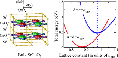
The copper oxide ACuO2 with infinite layer structure Siegrist:nat88 depicted in Fig. 1 can be regarded as a defect perovskite with ordered oxygen vacancies. It consists of positively charged A2+ and negatively charged CuO layers. Because all of the oxygen sites in the AO plane are vacant, there are Cu-O bonds in the plane but none in the direction. The missing atoms and bonds lead to a reduction of the lattice constant in the direction, reducing the symmetry from cubic in STO to tetragonal in ACO. The lattice constant of ACO increases as the ion radius increases in the series A = Ca, Sr, Ba. The calculated values given in Table 1 agree well with experiment and SCO is seen to have the smallest lattice mismatch with STO. Though a complex orthorhombic structure for SCO can also be synthesized Motoyama:prl96 , only the infinite layer structure is taken into consideration in thin film growth experiments Triscone:rpp97 ; Koster:jpcm08 ; Millis:prb10 ; Huijben:arxiv10 , thus we refer here to the infinite layer structure as the bulk structure and neglect other possibilities in this paper.
| SrTiO3 | 3.87 | 3.87 | 3.95 | 3.95 | 3.905 | 3.905 |
|---|---|---|---|---|---|---|
| CaCuO2 | 3.77 | 3.08 | 3.87 | 3.20 | 3.853 111Ref.Kobayashi:jssc97, | 3.177 111Ref.Kobayashi:jssc97, |
| SrCuO2 | 3.84 | 3.38 | 3.95 | 3.47 | 3.926 222Ref.Takano:physc89, | 3.432 222Ref.Takano:physc89, |
| BaCuO2 | 3.92 | 3.68 | 4.03 | 3.84 |
Including an on-site Coulomb repulsion term only slightly affects the calculated lattice constant, and can reproduce the observed antiferromagnetic insulating (AF-I) ground state Vaknin:prb89 with an energy gap located between filled oxygen bands and an unfilled minority spin Cu band Anisimov:prb91 . Because its nodes point toward neighbouring oxygen atoms, the orbital hybridizes strongly with the oxygen states and is pushed up in energy. The resulting Cu2+ configuration corresponds to all Cu orbitals being filled except for the minority spin orbital. This is apparent in the surfaces of constant magnetization density plotted in Fig. 1 where the spin density on the oxygen atoms also illustrates the AF superexchange coupling between neighbouring Cu ions. The hybridization is mainly confined to the CuO2 plane and does not affect the ionic character of the A2+ and CuO layers so the electrostatic instability of ACuO2 thin films still exists by analogy with LAO thin films.
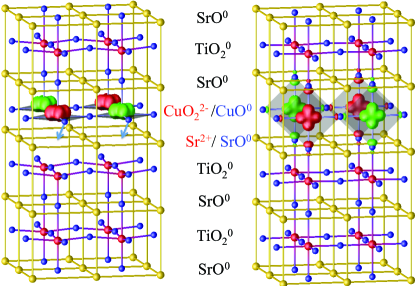
ACuO2 thin films: When SCO is grown on an STO substrate, it is assumed that positively charged A2+ and negatively charged CuO layers alternate Triscone:rpp97 . Because this planar (“CuO2”) structure will lead to an electrostatic instability, we also consider a chain type (“CuO”) structure that is formed by moving one oxygen atom from the CuO layer to the oxygen vacancy position in the A2+ layers as illustrated in Fig. 2 for the case of SCOSTO multilayers. This results in a thin film consisting of uncharged SrO0 and chain-type CuO0 layers that does not suffer from an electrostatic instability but at the expense of strain (Fig. 1). For sufficiently thick films, we expect the planar structure to be most stable. It is not clear a priori what will occur for thin films of thickness .
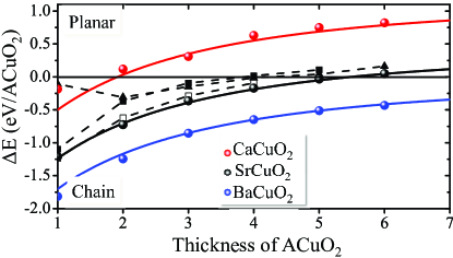
To answer this question, we calculate the energy difference, as a function of . As shown in Fig. 3, depends strongly on both and on the cation A. For SrCuO2 thin films grown on a lattice matched STO substrate, it increases gradually from -1.2 to +0.05 eV per unit cell, as the thickness increases from one to six unit cells. Since both structures have the same stoichiometry, the sign of is a direct measure of their relative stability. Below a critical thickness of about five unit cells, chain type thin films are energetically favourable; above it, planar type films are more stable. In the cation series CaSrBa, decreases but depends on thickness in the same way for all ACuO2 thin films. Similar behavior is found for multilayers and freestanding thin films so surface or interface effects are not essential for a qualitative understanding. We then decompose as , where () denotes the electrostatic energy (density) induced by the instability of planar type thin films and is the chemical bonding energy caused by the oxygen atom moving to form a strained chain-type structure.
The planar thin films are terminated with positively charged Sr2+ and negatively charged CuO surfaces with nominal areal charge densities where is the in-plane lattice constant. They can be modeled as parallel plate capacitors Nakagawa:natm06 ; Goniakowski:rpp08 ; Bristowe:prb09 ; Chen:prb10 ; Zhong:prb10 ; Millis:prb10 ; Goniakowski:prl07 in which the plates are separated by a thickness of bulk material with dielectric constant . The electrostatic energy density associated with the electric field between the plates is or approximately eV per unit cell, where is the dielectric constant of vacuum. This constitutes a strong instability that will drive charge transfer that depends on the thickness and electronic structure of the thin films Millis:prb10 . If we assume a rigid flat band approximation with constant density of states , the transferred charge is . As a result of the screening by the transferred charge, the residual electrostatic energy density becomes , where the screening factor clearly depends on and thin film thickness . For a large gap insulator with , is a constant 111Note1. For a good metal with a large , approaches zero. For a small band gap semiconductor with a moderate , vanishes when is large, consistent with bulk limits; if is reduced, less charge will be transferred and consequently will be enhanced. When the films are very thin, charge transfer cannot take place to quench the instability.
In that case, can be quenched by displacing oxygen atoms to form a chain-type structure as indicated in Fig. 2. Because the resulting structure corresponds to a strained ACuO2 thin film grown in a (100) orientation on a (001) STO substrate (rhs of Fig. 2), rather than with a conventional (001) orientation (lhs of Fig. 2), doing so will change the bonding energy . The two types of thin film only differ in terms of strain. To estimate the strain energy of planar type thin films, we fix the in-plane lattice constant of bulk ACuO2 at and minimize the total energy with respect to . For chain type thin films, we consider and as the in-plane lattice constants, fix them to be equal to and minimize with respect to , as shown in Fig.1. The energy difference per unit cell between the two minima is eV for SrCuO2, 1.19 eV for CaCuO2, and -0.01 eV for BaCuO2.
As shown in Fig. 3, can be fit very well using these values for and values of /V and in the modified parallel plate capacitor model for . The very good fit indicates that the competition between the two structures can be represented in terms of electronic and atomic reconstructions and that charge transfer can occur to partly screen the electrostatic instability without altering the atomic structures. However, as the films become thinner, the effect of screening decreases. For fewer than about five unit cells of SCO on STO, the widely assumed planar type thin film cannot be stabilized because of the instability. In spite of a considerable cost in strain energy, the chain type thin film should become energetically favorable because of the lowering of the electrostatic polarization energy .
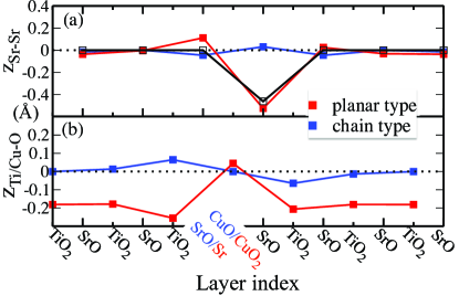
Atomic and electronic structure: To discuss the atomic and electronic properties of the novel chain-type thin films, we focus on the multilayers shown in Fig. 2 with a single unit cell of SCO sandwiched between five unit cells of STO. The parallel behaviour of the multilayer and thin film curves (black spheres and squares) in Fig. 3 indicates that the essential physics is the same so we can dispense with discussing the effect of dangling bonds at the free surface. In the chain-type film, there are stiff Cu-O bonds in the growth direction. Because of this, the multilayer containing chain-type SCO is almost 0.5 Å longer in the direction than that containing planar SCO. This is illustrated in Fig. 4(a) where the spacing between layers containing Sr atoms is plotted. Measurement of this spacing should be possible and would provide experimental evidence for chain type thin films. The presence of zigzag Ti-O buckling in Fig. 2 and 4(b) in the planar-type films is a strong indicator of internal electric fields Pentcheva:prl09 ; Bristowe:prb09 ; Chen:prb10 ; Zhong:prb10 that should be observable in structural studies. 222note2
The ground state of the planar-type SCO film is an AF metal. Consistent with a previous LDA+U calculation for YBa2Cu3O6 interfaces with STO Pavlenko:prb07 , we find that the orbital character of the Cu2+ minority spin hole is largely unchanged by the polar nature of thin films and the presence of apical oxygen atoms in the STO substrate that leads to Cu-O-Ti type bonding. In contrast, the ground state of the chain-type film is an AF insulator with a localized magnetic moment of 0.6 on Cu ions and an energy gap of 1.6 eV. The energy gap between filled O states and an unfilled minority spin Cu state will decrease on increasing the thickness of the SCO film.The unfilled Cu orbital character will be , as shown in Fig. 2, because the Cu ions are still in a CuO4 square planar configuration surrounded by four oxygen atoms in the - plane rather than the original, bulk - plane. Our results suggest an explanation for the orbital observed at the YBa2Cu3OLaMnO3 interface Chakhalian:sc07 ; the electrostatic instability of CuO2 planes Koster:jpcm08 ; Millis:prb10 may be driving oxygen atoms (or vacancies) to move and effectively tilt the CuO4 square towards the direction, favoring orbitals pointing in that direction. The polar nature of CuO2 planes may play a key role in the structure and properties of ultrathin films and interfaces of HTS cuprates.
Conclusion: Using first-principles calculations, we predict that a polar electrostatic instability will lead to chain type structures being preferred when films of ACuO2 are sufficiently thin and interpret this with a parallel plate capacitor model including charge transfer. As the polar film is made thinner, less charge can be transferred, the residual electrostatic energy increases, and formation of non-polar chain-type structures becomes an energetically favorable way to resolve the instability without changing the stoichiometry. Similar considerations can be applied to LAOSTO. Although pure charge transfer can avoid the “polar catastrophe”Nakagawa:natm06 ; Pentcheva:prl09 , it can not fully quench the electrostatic instability. A large residual electrostatic energy, especially in the low thickness LAO regime, will drive the formation of oxygen vacancies or other defects.
This work was supported by “NanoNed”, a nanotechnology programme of the Dutch Ministry of Economic Affairs. This work is also part of the research programs of “Stichting voor Fundamenteel Onderzoek der Materie” (FOM) and the use of supercomputer facilities was sponsored by the “Stichting Nationale Computer Faciliteiten” (NCF), both financially supported by the “Nederlandse Organisatie voor Wetenschappelijk Onderzoek” (NWO).
References
- (1) S. Okamoto and A. J. Millis, Nature 428, 630 (2004)
- (2) A. Ohtomo and H. Y. Hwang, Nature 427, 423 (2004)
- (3) S. Thiel, G. Hammerl, A. Schmehl, C. W. Schneider, and J. Mannhart, Science 313, 1942 (2006)
- (4) M. Huijben, A. Brinkman, G. Koster et al., Adv. Mat. 21, 1665 (2009)
- (5) N. Nakagawa, H. Y. Hwang, and D. A. Muller, Nature Materials 5, 204 (2006)
- (6) J. Goniakowski, F. Finocchi, and C. Noguera, Rep. Prog. Phys. 71, 016501 (2008)
- (7) J. Chakhalian, J. W. Freeland, H.-U. Habermeier et al., Science 318, 1115 (2007)
- (8) J. Junquera and P. Ghosez, Nature 422, 506 (2003)
- (9) Z. Zhong and P. J. Kelly, Europhys. Lett. 84, 27001 (2008)
- (10) Z. S. Popović, S. Satpathy, and R. M. Martin, Phys. Rev. Lett. 101, 256801 (2008)
- (11) R. Pentcheva and W. E. Pickett, Phys. Rev. Lett. 102, 107602 (Mar 2009)
- (12) N. C. Bristowe, E. Artacho, and P. B. Littlewood, Phys. Rev. B 80, 045425 (2009)
- (13) H. Chen, A. Kolpak, and S. Ismail-Beigi, Phys. Rev. B 82, 085430 (2010)
- (14) G. Herranz, M. Basletić, M. Bibes et al., Phys. Rev. Lett. 98, 216803 (2007)
- (15) A. S. Kalabukhov, Y. A. Boikov, I. T. Serenkov et al., Phys. Rev. Lett. 103, 146101 (2009)
- (16) S. A. Chambers, M. H. Engelhard, V. Shutthanandan et al., Surface Science Reports 65, 317 (2010)
- (17) Z. Zhong, P. X. Xu and P. J. Kelly, Phys. Rev. B 82, 165127 (2010)
- (18) T. Siegrist, S. M. Zahurak, D. W. Murphy, and R. S. Roth, Nature 334, 231 (1988)
- (19) M. Takano, Y. Takeda, H. Okada, M. Miyamoto, and T. Kusaka, Physica C 159, 375 (1989)
- (20) N. Kobayashi, Z. Hiroi, and M. Takano, J. Solid State Chem. 132, 274 (1997)
- (21) J.-M. Triscone and O. Fischer, Rep. Prog. Phys. 60, 1673 (1997)
- (22) M. Huijben et al., e-print arXiv:cond-mat/1008.1896v1
- (23) A. J. Millis and D. G. Schlom, Phys. Rev. B 82, 073101 (2010)
- (24) E. Bousquet, M. Dawber, N. Stucki et al., Nature 452, 732 (2008)
- (25) N. A. Benedek and C. J. Fennie, Phys. Rev. Lett. 106, 107204 (2011)
- (26) P. E. Blöchl, Phys. Rev. B 50, 17953 (1994)
- (27) G. Kresse and D. Joubert, Phys. Rev. B 59, 1758 (1999)
- (28) S. L. Dudarev, G. A. Botton, S. Y. Savrasov et al., Phys. Rev. B 57, 1505 (1998)
- (29) V. I. Anisimov, J. Zaanen, and O. K. Andersen, Phys. Rev. B 44, 943 (1991)
- (30) N. Motoyama, H. Eisaki, and S. Uchida, Phys. Rev. Lett. 76, 3212 (1996)
- (31) G. Koster, A. Brinkman, H. Hilgenkamp et al., J. Phys.: Condens. Matter 20, 264007 (2009)
- (32) D. Vaknin, E. Caignol, P. K. Davies et al., Phys. Rev. B 39, 9122 (1989)
- (33) J. Goniakowski and C. Noguera, and L. Giordano, Phys. Rev. Lett. 98, 205701 (2007)
- (34) J. Goniakowski and C. Noguera, and L. Giordano, Phys. Rev. Lett. 93, 215702 (2004)
- (35) C. L. Freeman and F Claeyssens, and N. L Allan, and J. H Harding, Phys. Rev. Lett. 96, 066102 (2006)
- (36) C. Tusche and H. L. Meyerheim, and J. Kirschner, Phys. Rev. Lett. 99, 026102 (2007)
- (37) N. Pavlenko, I. Elfimov, T. Kopp, and G. A. Sawatzky, Phys. Rev. B 75, 140512 (2007)
- (38) consistent with “uncompensated polarity” in MgO films, see Goniakowski:prl07
- (39) Theoretical studies for MgO(111) Goniakowski:prl04 and ZnO Freeman:prl06 polar thin films predict analogous changes in atomic structures driven by electrostatic instabilities. Such changes have recently been observed Tusche:prl07 .