Low-energy silicon allotropes with strong absorption in the visible for photovoltaic applications
Abstract
We present state-of-the-art first-principle calculations of the electronic and optical properties of silicon allotropes with interesting characteristics for applications in thin-film solar cells. These new phases consist of distorted sp3 silicon networks and have a lower formation energy than other experimentally produced silicon phases. Some of these structures turned out to have quasi-direct and dipole-allowed band gaps in the range 0.8–1.5 eV, and to display absorption coefficients comparable with those of chalcopyrites used in thin-film record solar cells.
If Nature chose carbon as the scaffolding of life, mankind chose silicon as the building block of much of the high-technology of today. In fact, its advantages are many: silicon is the second most abundant element in the Earth’s crust, its processing is well controlled at the industrial level, and its electronic properties and defect physics are theoretically well understood. As an elemental substance, it is an intrinsic semiconductor that can readily be – and –doped with a multitude of different elements. This makes silicon the material of choice for applications in electronics.
Silicon is also the leading player in the important field of photovoltaic energy production. In fact, the large majority of the first-generation solar cells, based on a single - junction, use bulk silicon as absorber layer. Its band-gap ( eV at room temperature bludau1974 ) lies in the optimal interval of values to maximize energy conversion efficiency, according to the Schockley-Queisser limit shockley-queisser . However, the fact that the gap is indirect, and that the optical gap is larger than 3 eV, makes silicon a very bad absorber of sunlight lautenschlager1987 . Therefore, the absorbing layer has to be at least 100 m thick and, as a consequence, the crystal needs to be very pure, so that the mean-free path of the carriers is comparable with the size of the layer little1997 ; chopra2004 . This is a limiting factor in the reduction of the cost of photovoltaic modules.
Due to these well-known limitations, materials with better absorption coefficients in the visible have been put forward in the past years in order to replace silicon in thin-film solar cells repins2008 ; rau1999 ; todorov2010 ; redinger2011 . Emphasis has obviously been given to direct band-gap materials, with gaps between 1 and 1.5 eV and with absorption spectra that strongly overlap with the solar spectrum vidal2010 ; botti2011 ; aguilera2011 . However, and in spite of many spectacular advances, none of these materials has been able to dethrone silicon. Of course, the ideal solution would be to engineer silicon such that it absorbs strongly in the visible, in order to use thin-film technology and at the same time maintain the silicon-based processes that are currently employed. This would allow for thinner, flexible, and cheaper silicon solar cells.
Aiming at maximizing the spectral overlap, some authors have recently suggested different ways to manipulate the optical properties of silicon. Nanostructuring is a largely explored way to obtain direct-gap silicon by relaxing translational symmetry li2008 . However, the existence of a direct gap does not guarantee that transitions at the absorption edge are dipole allowed. Indeed, this is usually not the case in silicon nanostructures li2010 . D’Avezac et al. d-avezac2012 proposed recently an ultrathin silicon/germanium superlattice with excellent absorption properties. The experimental synthesis of such system requires, however, control of the growth of pure monolayers. Compensated doping of silicon obtained through substitutional impurities was also shown to increase by 25% the absorption of 10 m thick silicon layers samsonidze2011 . Nevertheless, doping is expected to introduce recombination centers detrimental for the performances of the device.
Other works investigated the possibility to modify the band structure of silicon by using allotropic phases with different crystal symmetries malone2008R ; malone2008 ; malone2010 ; malone2012 . The most stable phase of silicon, at ambient conditions, is the cubic diamond structure. High pressure phases have been experimentally studied up to 248 GPa duclos1990 , and several calculations of the phase transitions are present in literature needs1995 ; pfrommer1997 ; mujica2003 . Upon increase of pressure silicon exhibits a series of phase transitions: from cubic diamond to -Sn at around 12 GPa, from -Sn to orthorhombic (Imma symmetry) imma and then to simple hexagonal at 13–16 GPa, from simple hexagonal to an orthorombic Cmca phase at about 38 GPa hanfland1999 , from Cmca to hexagonal close pack at 42 GPa, and finally to face-centered cubic at 78 GPa. It has been known for more than 20 years that, upon slow release of pressure from the -Sn structure, silicon transforms into the rombohedral R8 and the body-centered BC8 crystals, characterized by distorted sp3 bondingsneeds1995 ; pfrommer1997 ; mujica2003 . R8 and BC8 are metastable phases, as they keep existing at ambient conditions. If BC8 silicon is heated to temperatures in the range from 200 to 600 , it transforms to another metastable phase: the lonsdaleite hexagonal diamond lonsdaleite . Two other phases, the so-called Si-VIII and Si-IX structures, were observed experimentally upon rapid release of pressure from -Sn silicon zhao1986 . However, their crystal lattices were not fully characterized. Nanoindetation experiments gave evidences of another phase, known as Si-XIII Si-XIII , although also in this case very little information is available on its crystal structure. Other meta-stable phases that lay close in energy to cubic diamond silicon have been proposed theoretically, using a multitude of methods BCT ; ST12 ; wang2010 ; malone2012 . Malone et al. calculated the band structure and the absorption spectrum one of these low-energy arrangements, charachterized by a body-centered-tetragonal (BCT) unit cell malone2010 . A similar study was carried out by the same authors also for the experimental R8 structure malone2008R . Unfortunately, BCT silicon did not show enhanced absorption properties in the visible if compared to cubic diamond silicon and R8 turned out to have a too small gap (0.24 eV) for photovoltaic applications. However, the low-pressure phase diagram of silicon is still relatively unexplored, which makes us believe that there might exist unexplored silicon phases with optical properties suitable for thin-film photovoltaics.
In this paper we present the results of a structural prediction search that leads to a number of previously unknown, low-energy, phases of silicon that have excellent properties for photovoltaic applications, with quasi-direct band-gaps between 1–1.5 eV, and excellent absorption properties for solar light. Note that the band gap imposes an upper bound on the open-circuit voltage of the device, implying that too small indirect band-gap compounds should be discarded. All structures we selected have a total energy higher than the one of cubic silicon by less than 0.15 eV per atom. This restriction assures that the experimental synthesis of these structures is energetically plausible.
The silicon crystalline arrangements under investigation were found by performing a structural relaxation of low-enthalpy carbon primitive cells with 8 atoms, which we had previously calculated prl_Z-carbon_2012 by applying a very efficient structural prediction algorithm, the minima hopping method (MHM) goedecker_2004 ; amsler_2010 . The MHM was designed to obtain the low-enthalpy structures of a system given solely its chemical composition. The enthalpy surface is explored by performing consecutive short molecular dynamics escape steps followed by local geometry relaxations taking into account both atomic and cell variables. The initial velocities for the molecular dynamics trajectories are chosen approximately along soft mode directions, thus allowing efficient escapes from local minima and aiming towards low energy structures. The predictive power of this approach has already been demonstrated for a wide range of applications hellmann_2007 ; roy_2009 ; bao_2009 ; willand_2010 ; prl_Z-carbon_2012 ; prl_disilane_2012 . As carbon admits both and bonds, its phase diagram is much richer than the one of silicon. For this reason the low-enthalpy carbon allotropes found at low pressure provide a good structural database for silicon analogues. Indeed, we observed that the carbon structures with bonds turn out to be unstable and relax into a different geometry with arrangement.
| structure | spc group | /atom | C analogue | ||
|---|---|---|---|---|---|
| Z | 65 | 0.06 | 0.72 | 1.22 | Ref. prl_Z-carbon_2012,; PRBR_C222,; PRL_Zcarbontwo, |
| M | 12 | 0.07 | 0.46 | 0.99 | Ref. M12carbon_Oganov, |
| M-10 | 10 | 0.08 | 0.97 | 1.40 | Ref. Cmcm_PRB,; prb_M10_carbon_2012, |
| C2221 | 20 | 0.08 | 0.90 | 1.39 | Ref. PRBR_C222, |
| Imma(2) | 74 | 0.12 | 0.63 | 1.15 | – |
| Cmcm | 63 | 0.13 | 0.32 | 0.83 | Ref. Cmcm_PRB, |
| P-1 | 2 | 0.13 | 0.28 | 0.75 | – |
| P21/c | 14 | 0.14 | 0.73 | 1.29 | – |
The evaluation of energies and forces required for the MHM were performed within density functional theory (DFT) using the ABINIT code abinit , with simulation cells of 8 carbon atoms at 15 GPa. The lowest energy silicon analogues were further relaxed and characterized using the VASP code vasp . We selected our -point grids to ensure an accuracy of 0.01 eV in the total energy, and all forces were converged to better than 0.005 eV/Å. To approximate the exchange-correlation functional of DFT we used the Perdew-Burke-Ernzerhof (PBE) PBE generalized gradient approximation.
In an energy interval of 0.15 eV per atom (around 1740 K) from the diamond structure, and ignoring the well-known cubic diamond and hexagonal diamond silicon, we found a total of 16 structures. We checked the stability of these phases by calculating their phonon band structure, in order to make sure that all phonon modes are real. We note that the experimentally known meta-stable phases of silicon, R8 and BC8, have higher energies than the phases considered here. Interestingly, also the most studied theoretical meta-stable phases (ST12, BCT, Ibam etc.) are energetically less favored than the new structures presented in this work.
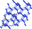
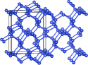
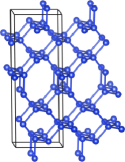
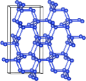
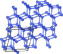
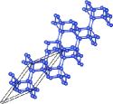
All our structures have bonding, and are semiconducting with Kohn-Sham PBE (indirect) gaps ranging from 0.3 to 1.2 eV. Some of the carbon analogues can already be found in the literature (see Table 1). It is noticeable that none of the around 300 semiconducting structures identified by our simulation footnote has a direct quasi-particle gap. Nevertheless, several of them exhibit a quasi-direct gap. The lowest-energy structures we found with promising quasiparticle gaps are listed, together with their space group number and the value of the calculated gaps, in Table 1. The corresponding atomic arrangements are depicted in Fig. 1.
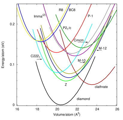
In Fig. 2 we show the total energy per atom as a function of volume per atom for the new silicon allotropes found in this study. For the sake of comparison we included the energy curves of some well known phases of silicon, e.g., cubic diamond silicon, a clathrate, the BC8 and R8 structures.
By inspection of Fig. 2 and Table 1 we can easily deduce that, among the novel silicon structures, the lowest energy allotropes is Z-silicon, followed by M and M-10 silicon. These crystal structures have carbon counterparts that are thought to play an important role in cold-compressed graphite prl_Z-carbon_2012 . The volumes per atom at equilibrium of the new structures are between 20 and 22 Å3, which places them in an intermediate position between the open clathrates and the experimentally observed BC8 and R8 structures.
In order to characterize the fundamental and optical band gaps, together with the absorption spectra, we performed perturbative hedin calculations and we solved the Bethe-Salpeter equation BSE ; lucia1998 using the abinit package abinit . We want to stress that we employed the most accurate methods available in the community to study electronic excitations, that have proved to give excellent results for a wide range of semiconductors and insulators. aulbur ; review-lucia In particular, the BSE absorption spectrum of cubic diamond silicon lucia1998 is in excellent agreement with experimental measurements lautenschlager1987 , thanks to the inclusion of excitonic effects. We used Troullier-Martins norm-conserving pseudopotentials TM and the PBE exchange-correlation functional PBE . The planewave cut-off energy for all runs was 15 Hartree. For calculations the cutoff of the dielectric matrix was set to 5 Hatree and we needed 12 states per atom, together with the method of Bruneval and Gonze, to achieve a convergence of around 0.05 eV in the band gap. For the Bethe-Salpeter calculations we used a cutoff of 2.5 Hartree for the dielectric matrix and a k-point spacing of around 0.012 in reciprocal lattice vector units for the shifted k-point mesh. This criterion yields a 141414 shifted grid for the diamond structure.
All the corrections to the Kohn-Sham PBE band structures can be approximated by a rigid shift of the conduction bands, as they are fairly independent of the k-points. Furthermore, this rigid shift does not change significantly among the different crystal lattices, ranging from 0.4 to 0.6 eV, even if the Kohn-Sham gaps exhibit larger variations. By inspecting the values for the indirect gaps in Table 1 we can observe that several silicon structures have a gap in the optimal frequency interval for maximizing photovoltaic efficiency. However, one should not forget that all the gaps that we calculated are indirect, even if in many cases the direct gaps are much smaller than in the cubic diamond phase. This fact suggests that it is conceivable that the absorption edge for direct transitions of these metastable allotropes is at significantly lower energies than in conventional silicon. However, information on the band structure alone is not conclusive, since the dipole matrix elements between states close to the valence band maximum and the conduction band minimum can be very small and suppress light absorption close to the absorption edge. In view of that, we performed accurate calculations of the absorption spectra by solving the Bethe-Salpeter equation.
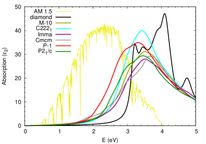
In Fig. 3 we show the calculated absorption spectra of the allotropes that are most promising for applications in solar cells. The calculated absorption spectrum of the cubic diamond phase is also shown for comparison, together with the reference air mass (AM) 1.5 solar spectral irradiance. Note that indirect absorption contributions, which arises from phonon assisted interband transitions are not included in our calculations. All new structures start to absorb very close to their direct gap, with the result that their absorption spectra overlap significantly with the solar spectrum. Remarkably, the absolute optical absorption between 1.5 and 3 eV strictly is comparable to that of Cu(In,Ga)Se2 compounds, that are regarded as excellent absorbers for thin-film solar cell technology exp-abs-CIGS . This indicates that these new silicon phases could potentially be employed in highly efficient silicon thin-film solar panels.
If we make a critical evaluation of all calculated properties, we can conclude that the most promising allotropes are the M-10 and the C2221. In fact, their total energies per atom are particularly low, their indirect gap is 1.4 eV, while the direct gap is only slightly larger (1.5 eV for M-10 and 2.0 eV for C2221). Moreover, absorption is dipole allowed starting from the absorption edge, as it is revealed by the long tails of their BSE absorption spectra in the visible.
In conclusion, we predict several novel metastable phases of silicon, obtained through a structural search based on carbon analogues found using the minima hopping method. We filtered the most promising structures for use in thin-film photovoltaics by imposing that the total energy per atom does not differ by more than 0.15 eV from the total energy per atom of cubic diamond silicon. Moreover, we imposed that the fundamental band gap is in the range 1.0–1.5 eV. Some of the new structures revealed a strong absorption in the visible, with absorption coefficients comparable to those of chalcopyrite absorbers used in thin-film record solar cells. These results call for further experimental studies of the low-pressure phase diagram of silicon, and could open new routes to design highly efficient thin-film silicon solar cells.
JAFL acknowledges the CONACyT-Mexico. MALM acknowledges support from the French ANR (ANR-08-CEXC8-008-01). Financial support provided by the Swiss National Science Foundation is gratefully acknowledged. Computational resources were provided by IDRIS-GENCI (project x2011096017) in France and the Swiss National Supercomputing Center (CSCS).
References
- (1) W. Bludau, A. Onton, and W. Heinke, J. Appl. Phys. 45, 1846 (1974).
- (2) W. Shockley and H. J. Queisser, J. Appl. Phys. 32, 510 (1961).
- (3) P. Lautenschlager, M. Garriga, L. Vina, and M. Cardona, Phys. Rev. B 36, 4821 (1987).
- (4) R.G. Little and M.J. Nowlan, Prog. Photovoltaics 5, 309 (1997).
- (5) K.L. Chopra, P.D. Paulson, and V. Dutta, Prog. Photovoltaics 12, 69 (2004).
- (6) I. Repins, M.A. Contreras, B. Egaas, C. DeHart, J. Scharf, C.L. Perkins, B. To, and R. Noufi, Prog. Photovoltaics 16, 235 (2008).
- (7) U. Rau and H. Schock, Appl. Phys. A 69, 131 (1999).
- (8) K. Todorov, K. B. Reuter, and D. B. Mitzi, Adv. Mater. (Weinheim, Ger.) 22, E156 (2010).
- (9) A. Redinger, D. M. Berg, P. J. Dale, and S. Siebentritt, J. Am. Chem. Soc. 133, 3320 (2011).
- (10) J. Vidal, S. Botti, P. Olsson, J.-F. Guillemoles, and L. Reining, Phys. Rev. Lett. 104, 056401 (2010).
- (11) S. Botti, D. Kammerlander, and M.A.L. Marques Appl. Phys. Lett. 98, 241915 (2011).
- (12) I. Aguilera, J. Vidal, P. Wahnón, L. Reining, and S. Botti Phys. Rev. B 84, 085145 (2011).
- (13) D.X. Li and J.Y. Feng, Appl. Phys. Lett. 92, 243117 (2008).
- (14) D. Li, L. Lin, and J. Feng, Physica (Amsterdam) 42E, 1583 (2010).
- (15) M. d’Avezac, J.-W. Luo, T. Chanier, and A. Zunger, Phys. Rev. Lett. 108, 027401 (2012).
- (16) G. Samsonidze, M.L. Cohen, and S. G. Louie, Phys. Rev. B 84, 195201 (2011).
- (17) B.D. Malone, J.D. Sau, and M.L. Cohen, Phys. Rev. B 78, 161202(R) (2008).
- (18) B.D. Malone, J.D. Sau, and M.L. Cohen, Phys. Rev. B 78, 035210 (2008).
- (19) B.D. Malone, S.G. Louie, and M.L. Cohen, Phys. Rev. B 81, 115201 (2010).
- (20) B.D. Malone and M.L. Cohen, Phys. Rev. B 85, 024116 (2012).
- (21) S.J. Duclos, Y.K. Vohra, and A.L. Ruoff, Phys. Rev. B 41, 12021 (1990); M.I. McMahon and R.J. Nelmes, Phys. Rev. B 47, 8337 (1993).
- (22) R.J. Needs and A. Mujica, Phys. Rev. B 51 9652 (1995).
- (23) B.G. Pfrommer, M. Côté, S.G. Louie, and M.L. Cohen, Phys. Rev. B 56, 6662 (1997).
- (24) A. Mujica, S. Radescu, A. Muñoz, and R. Needs, Phys. Status Solidi B 223, 379 (2001); A. Mujica, A. Rubio, A. Muñoz, and R. J. Needs, Rev. Mod. Phys. 75, 863 (2003).
- (25) M. I. McMahon, R. J. Nelmes, N. G. Wright, and D. R. Allan, Phys. Rev. B 50, 739 (1994).
- (26) M. Hanfland, U. Schwarz, K. Syassen, and K. Takemura, Phys. Rev. Lett. 82, 1197 (1999).
- (27) J.M. Besson, E. H. Mokhtari, J. Gonzalez, and G. Weill, Phys. Rev. Lett. 59, 473 (1987); F.P. Bundy and J.S. Kasper, Science 139, 340 (1963); B. R. Wu, Phys. Rev. B 61, 5 (2000).
- (28) Y.-X. Zhao, F. Buehler, J.R. Sites, and I.L. Spain, Solid State Commun. 59, 679 (1986).
- (29) D. Ge, V. Domnich, and Y. Gogotsi, J. Appl. Phys. 95, 2725 (2004); S. Ruffell, B. Haberl, J.E. Bradby, and J.S. Williams, J. Appl. Phys. 105, 093513 (2009).
- (30) Y. Fujimoto, T. Koretsune, S. Saito, Y. Miyake, and A. Oshiyama, New J. Phys. 10, 083001 (2008).
- (31) R. J. Nelmes, M. I. McMahon, N. G. Wright, D. R. Allan, and J. S. Loveday, Phys. Rev. B 48, 9883 (1993).
- (32) Y. Wang, J. Lv, L. Zhu, and Y. Ma, Phys. Rev. B 82, 094116 (2010).
- (33) M.A. Zwijnenburg, K.E. Jelfs, and S.T. Bromley, Phys. Chem. Chem. Phys. 12, 8505 (2010).
- (34) M. Amsler, J.A. Flores-Livas, L. Lehtovaara, F. Balima, S.A. Ghasemi, D. Machon, S. Pailhes, A. Willand, D. Caliste, S. Botti, A. San Miguel, S. Goedecker, and M.A.L. Marques, Phys. Rev. Lett. 108, 065501 (2012).
- (35) Goedecker, J. Chem. Phys. 120, 9911 (2004).
- (36) M. Amsler and S. Goedecker, J. Chem. Phys. 133, 224104 (2010).
- (37) W. Hellmann, R. G. Hennig, S. Goedecker, C. J. Umrigar, B. Delley, and T. Lenosky, Phys. Rev. B 75, 085411 (2007).
- (38) S. Roy, S. Goedecker, M. J. Field, and E. Penev, J. Phys. Chem. B 113, 7315 (2009).
- (39) K. Bao, S. Goedecker, K. Koga, F. Lançon, and A. Neelov, Phys. Rev. B 79, 041405 (2009).
- (40) A. Willand, M. Gramzow, S.A. Ghasemi, L. Genovese, T. Deutsch, K. Reuter, and S. Goedecker, Phys. Rev. B 81, 201405 (2010).
- (41) J.A. Flores-Livas, M. Amsler, T.J. Lenosky, L. Lehtovaara, S. Botti, M.A.L. Marques, and S. Goedecker, Phys. Rev. Lett. 108 117004 (2012).
- (42) G. Kresse and J. Furthmüller, Comput. Mater. Sci. 6, 15 (1996); Phys. Rev. B 54, 11169 (1996).
- (43) J. P. Perdew, K. Burke, and M. Ernzerhof, Phys. Rev. Lett. 77, 3865 (1996).
- (44) G. B. Adams, M. O’Keeffe, A. A. Demkov, O. F. Sankey, and Y.-M. Huang, Phys. Rev. B 49, 8048 (1994).
- (45) M. Amsler, J.A. Flores-Livas, S. Botti, M.A.L. Marques, S. Goedecker, arXiv:1202.6030v1 [cond-mat.mtrl-sci]
- (46) All structures found in this study, together with symmetry analysis, can be found at http://www.tddft.org/bmg/physics/structures/Si-00GPa/.
- (47) L. Hedin, Phys. Rev. 139, A796 (1965); L. Hedin and S. Lundqvist, Solid State Phys. 23, 1 (1970).
- (48) E.E. Salpeter and H.A.Bethe, Phys. Rev. 84, 1232 (1951).
- (49) S. Albrecht, L. Reining, R. Del Sole, and G. Onida, Phys. Rev. Lett. 80, 4510 (1998).
- (50) X. Gonze, G.-M. Rignanese, M. Verstraete, J.-M. Beuken, Y. Pouillon, R. Caracas, F. Jollet, M. Torrent, G. Zerah, M. Mikami, Ph. Ghosez, M. Veithen, J.-Y. Raty, V. Olevano, F. Bruneval, L. Reining, R. Godby, G. Onida, D. R. Hamann, and D. C. Allan, Z. Kristallogr. 220, 558 (2005).
- (51) W.G. Aulbur, L. Jönsson, and J.W. Wilkins, in Solid State Physics, edited by H. Ehrenreich and F. Spaepen (Academic, New York) 54, 1 (2000).
- (52) G. Onida, L. Reining, and A. Rubio, Rev. Mod. Phys. 74, 601 (2002).
- (53) N. Troullier and J. L. Martins, Phys. Rev. B 43, 1993 (1991).
- (54) ASTM Standard G173–03, 2008, “Standard Tables for Reference Solar Spectral Irradiances: Direct Normal and Hemispherical on 37∘ Tilted Surface,” ASTM International,West Conshohocken, PA, 2008, doi: 10.1520/G0173-03R08, [www.astm.org].
- (55) M.I. Alonso, K. Wakita, J. Pascual, M. Garriga, and N. Yamamoto, Phys. Rev. B 63, 075203 (2001); S. Levchenko, N.N. Syrbu, V.E. Tezlevan, E. Arushanov, J.M. Merino, and M Léon, J. Phys. D: Appl. Phys. 41, 055403 (2008).
- (56) Q. Li, Y. Ma, A. R. Oganov, H. Wang, H. Wang, Y. Xu, T. Cui, H. K. Mao, G. Zou, Phys. Rev. Lett. 102, 175506 (2009).
- (57) A. O. Lyakhov and A. R. Oganov, Phys. Rev. B 84, 092103 (2011).
- (58) Z. Zhao, B. Xu, X.-F. Zhou, L.-M. Wang, B. Wen, J. He, Z. Liu, H.-T. Wang, Y. Tian, Phys. Rev. Lett. 107, 215502 (2011).
- (59) D. Selli, I. A. Baburin, R. Martonak, and S. Leoni, Phys. Rev. B 84, 161411(R), (2011)