,
Few Electron Limit of n-type Metal Oxide Semiconductor Single Electron Transistors
Abstract
We report electronic transport on n-type silicon Single Electron Transistors (SETs) fabricated in Complementary Metal Oxide Semiconductor (CMOS) technology. The n-MOSSETs are built within a pre-industrial Fully Depleted Silicon On Insulator (FDSOI) technology with a silicon thickness down to 10 nm on 200 mm wafers. The nominal channel size of 2020 nm2 is obtained by employing electron beam lithography for active and gate levels patterning. The Coulomb blockade stability diagram is precisely resolved at 4.2 K and it exhibits large addition energies of tens of meV. The confinement of the electrons in the quantum dot has been modeled by using a Current Spin Density Functional Theory (CS-DFT) method. CMOS technology enables massive production of SETs for ultimate nanoelectronics and quantum variables based devices.
1 Introduction
The fabrication of semiconductor quantum dots in CMOS technology provides the ground for integration of existing microelectronics with ultimate nanoelectronics for quantum circuits. We report on the realization of Single Electron Transistors (SETs) in pre-industrial CMOS technology at the limiting channel size of 2020 nm2 and on the characterization of the quantum transport at cryogenic temperature, enabling the detection of the first electron in the SET.
Silicon SETs based on CMOS technology represent a natural environment for realizing scalable electron spin and orbital quantum devices for quantum information processing [1] because of long coherence times [2] and scalability. The need to create a workable Hilbert space with good quantum numbers [3] at increasingly high temperatures towards room temperature operability implies the reduction of the size of the quantum dots down to the current limits of fabrication. [4] The drawback is an increasing sensitivity of the confinement potential imposed by the control gate to impurities and roughness, and a consequent impact on the electronic shell structure of the quantum dot. In the past, some approaches for creating single electron silicon quantum dots have been explored, including the employment of gate induced two dimensional electron gas (2DEG) at the Si/SiO2 interfaces [5], global gate controlled edge roughness of an ultra small nanowire [6], local gate equipped underlap geometry where the gate is not at the state-of-the-art and consequently enforces the use of large gate voltages [7], triple-layer gate stacks [8] and Si/SiGe modulation-doped heterostructures [9].
Our approach consists in confining electrons in a well defined by lateral doping modulation. Indeed barriers are consequence of undoped silicon below spacers which are on both sides of the gate. [10] In the past, this approach has been exploited to fabricate compact double and triple quantum dots realized with only two gates. [11] The two main advantages are on one hand its compactness, as regard to state-of-the-art previous works on Si including additional upper gate [12], and on the other one the detection of a clear single electron regime.
The use of CMOS technology in quantum dot fabrication takes benefit from its reproducibility and reliability, as well as the co-integration of quantum circuits with traditional CMOS.
2 Fabrication of the devices
For a repeatability and reliability purpose, our MOSSETs are built within a pre-industrial Fully Depleted Silicon On Insulator (FDSOI) technology on 200 mm wafers. Only a few modules of the device are slightly modified, such as the gate stack and the source/drain (S/D) implantation. Since we aim to scale our MOSSET down to 20 nm in both gate length and gate width dimensions, electron beam lithography was used for active and gate levels patterning. That results with dots as small as 202010 nm3.
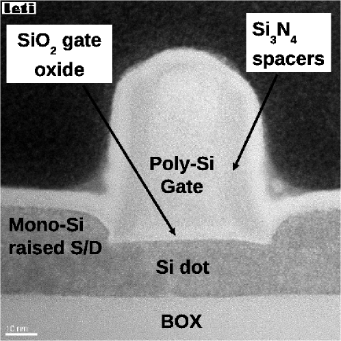
The undoped SOI layer is thermally thinned down to reach a silicon thickness of either 13 nm or 20 nm, depending on the sacrificial oxide thickness. After a first e-beam lithography, the SOI layer is etched to pattern the active area above the buried oxide (BOX). As a result of these first process steps a silicon nanowire is obtained. This mesa isolation allows to have wrapping gates on three sides of the nanowires. The silicon nanowire is then thermally oxidized on top and sides, resulting in a 4 nm thick SiO2 formation and a final silicon thickness =10 nm (17 nm) prior to polycrystalline silicon deposition. A second e-beam lithography is performed to define the tri-sided gate. Self-aligned silicon nitride spacers are formed on both the source- and drain-side of the gate to protect the underlying silicon from the subsequent doping steps. Epitaxy is then performed to raise the source and drain, and finally arsenic is implanted at high dose (leading to a typical concentration above 1020 cm-3) to create metallic-like S/D contacts. The resulting junction profile is such that the device is non-overlapped, i.e. the transistor’s channel is separated from the source and drain by the small low-doped region below the spacers. This non-overlapped geometry is responsible for the SET behavior [10]. Figure 1a shows a transmission electron micrograph of a tri-sided gate nanowire MOSSET coming from a wafer used for the morphological characterization with channel thickness =17 nm, oxide thickness =4 nm and gate length =22 nm realized with a process identical to the samples reported throughout the text.

(a)

(b)
3 Simulation of the electrostatic confinement
In order to evaluate the confinement of the electrons induced by the applied electrostatic potential we used a three dimensional self-consistent simulator based on Current Spin Density Functional Theory (CS-DFT) in the framework of the NanoTCAD ViDES package. [13, 14, 15, 16] It solves the many particle Schr dinger equation by means of CS-DFT, by transforming the many electron problem in a single-electron problem with exchange-correlation potential. It embraces the local density approximation and the effective mass approximation with parabolic bands. The method provides the ground state of the system for each occupation number of electrons. They fill the lowest single-particle Kohn-Sham eigenvalues calculated for each spin and each pair of the three valley pairs aligned to the main directions in the space.
The final shape of the confining potential energy is reached by self-consistently solving the Poisson equation. The effective nature of the confinement is due to the combination of the band alignment between the silicon and silicon dioxide and of the applied external potentials.
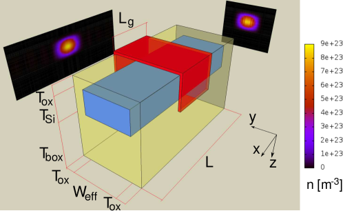
The SET is modeled as a silicon nanowire with length along the x direction and with a rectangular section of area on the y-z plane with source and drain contacts at the head and tail of the nanowire on the top of a silicon dioxide slab of thickness , see Figure 1b. The device has a tri-sided gate structure and the gate is insulated from the nanowire with a thick silicon dioxide layer.
The many particle problem is solved in the entire silicon nanowire and in a 1 nm-thick region inside the surrounding oxide. Potentials to the tri-sided gate, source and drain regions are applied whereas a zero electric field z-component boundary condition is forced at the bottom of the device. We simulate the electrostatic behavior of the SETs imposing an effective gate length = 22 nm, an effective width =10 nm to take into account the variability of the lithography process on the nominal length =20 nm and both the lithography process variability and the oxidation reduction on the nominal width =20 nm.
In Figure 1b the electron density in the central planes of the nanowire is reported as color-scaled planes, showing a strong confinement in the region under the gate contact biased at =26 mV when one electron is in the dot. The first addition energy which provides the energy separation between the one electron state and the two electrons state has been calculated. By using the effective size of =22 nm, =10 nm we determined an addition energy of =17 meV. Note that our simulations take into account all the couplings of the SET with the gate electrode but also with the source and drain contacts. Our approach does not take into account the possible disorder caused by the impurities and the interface roughness, which are expected to further enhance the confinement of the wavefunction in such small devices.
4 Quantum transport experimental results
The investigation of the electronic transport through the devices yields both the electron filling as a function of the QD gate voltage , as well as the addition energies needed to add the electron when electrons occupy the quantum dot. The characterization at the temperature =4.2 K of several nominally identical samples like those described in Section 2 demonstrate that the transistors operate as single electron devices, with relatively high addition energies.
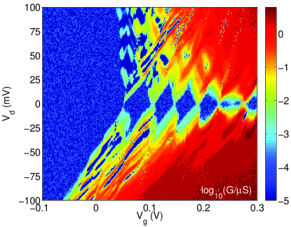
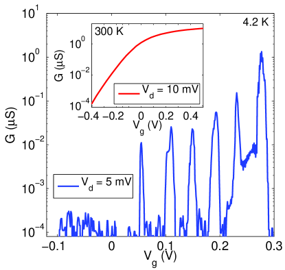
In Figure 2a the stability diagram of a typical device with of nm and nm is shown. The coupling with the source, drain and gate are aF, aF and aF respectively. The lever arm factor, which allows to convert the voltage spacing between the peaks into addition energies and which is defined as , assumes a value of 0.64. The first addition energy of the device shown in Figure 2a is = 30 meV. Figure 2b shows the Coulomb blockade observed from =0 up to a filling number of 6 in the range from -0.1 V to 0.3 V. In the inset the results of the conductance measurement performed at room temperature are reported.
In these small devices it is possible to reduce the electron occupancy of the quantum dot down to the empty state, hence the transition from to electron occupancy of the SET becomes observable, a key step towards single electron charge and spin manipulation.
The experimental confirmation is obtained by the lack of Coulomb diamond and any detectable current (up to =100 mV) below the first reported Coulomb oscillation at =40 mV. Moreover we notice that there is no significant shift between the threshold voltage obtained at =300 K ( -40 mV calculated as the maximum of the second derivative of the drain current with respect to the gate voltage, see inset of Figure 2b) and the gate voltage position of the first Coulomb peak at low temperature (= 40 mV), taking into account the thermal broadening at =300 K.
The presented samples are smaller than similar samples previously studied (,=30-40 nm, [10] and [17]). The silicon thickness (=10 nm) and the spacer length (11 nm) have been scaled down accordingly to obtain a good trade-off between the first electron orbital-electrodes coupling and a large Coulomb energy. By contrast in previously reported similar devices [10] the first electrons in the accumulation channel are not detected and the first measurable current is at significantly larger gate voltage than the threshold voltage at room temperature. On the contrary for similar samples but without nitride spacers [8] - and therefore smaller effective channel length - the first electrons are on shallow donors in the body of the silicon and detected at gate voltage much below the threshold voltage at room temperature. [18, 19] In that case there is no MOSSET effect in the accumulation channel.
Similar results have been obtained in nominally identical devices. Because of the residual disorder determined by the interface roughness, the electron wavefunction is further confined so the first addition energies are even larger than those predicted from the simulation of the devices and are subject to some variability. From the addition energies found in typical devices, an effective radius of less than 12-15 nm can be estimated.

(a)

(b)
5 Conclusions
Our results show that CMOS technology used allows reliable fabrication of single electron transistors with gate size of 2020 nm2. Strong confinement has been predicted by CSDFT simulations and a clearly resolved Coulomb blockade pattern at 4.2 K with high addition energies of more than 20 meV exceeds the simulated values. The fabrication of SETs in CMOS technology provides the possible ground for integration between traditional microelectronics and quantum circuit oriented nanoelectronics.
We acknowledges Prof. Giuseppe Iannaccone and Prof. Gianluca Fiori for providing the NanoTCAD ViDES simulator and for fruitful discussions.
M. F. thanks support by the ELIOS project granted by Cariplo Foundation.
S. R. thanks support by an ARC-Future Fellowship project ID: FT100100589.
G. C. T. thanks support by an ARC-DECRA Fellowship project ID: DE120100702
References
References
- [1] M. Friesen, P. Rugheimer, D. E. Savage, M. G. Lagally, D. W. van der Weide, R. Joynt, and M. A. Eriksson. Practical design and simulation of silicon-based quantum-dot qubits. Phys. Rev. B, 67:121301, 2003.
- [2] J. J. L. Morton, D. R. McCamey, M. A. Eriksson, and S. A. Lyon. Embracing the quantum limit in silicon computing. Nature, 479(7373):345–353, 11 2011.
- [3] M. Friesen, S. Chutia, C. Tahan, and S. N. Coppersmith. Valley splitting theory of sige/si/sige quantum wells. Phys. Rev. B, 75:115318, 2007.
- [4] S. Pauliac-Vaujour, R. Wacquez, C. Vizioz, T. Chevolleau, M. Pierre, B. Previtali, C. Comboroure, N. Bove, B. Roche, M. Vinet, X. Jehl, M. Sanquer, and P. Sixt. Patterning strategy for monoelectronic device platform in a complementary metal oxide semiconductor technology. Jpn. J. Appl. Phys., 50:06GF15, 2011.
- [5] M. Xiao, M. G. House, and H. W. Jiang. Parallel spin filling and energy spectroscopy in few-electron si metal-on-semiconductor-based quantum dots. Appl. Phys. Lett., 97:32103, 2010.
- [6] M. Kobayashi, K. Miyaji, and T. Hiramoto. On the origin of negative differential conductance in ultranarrow-wire-channel silicon single-electron and single-hole transistors. Jpn. J. Appl. Phys., 47:1813, 2008.
- [7] S. J. Shin, C. S. Jung, B. J. Park, T. K. Yoon, J. J. Lee, S. J. Kim, J. B. Choi, Y. Takahashi, and D. G. Hasko. Si-based ultrasmall multiswitching single-electron transistor operating at room-temperature. Appl. Phys. Lett., 97:103101, 2010.
- [8] W. H. Lim, C. H. Yang, F. A. Zwanenburg1, and A. S. Dzurak. Spin filling of valley-orbit states in a silicon quantum dot. Nanotechnology, 22:335704, 2011.
- [9] C. B. Simmons, M. Thalakulam, N. Shaji, L. J. Klein, H. Qin, R. Blick, D. E. Savage, M. G. Lagally, S. N. Coppersmith, and M. A. Eriksson. Single-electron quantum dot in si/sige with integrated charge sensing. Appl. Phys. Lett., 91:213103, 2007.
- [10] M. Hofheinz, X. Jehl, M. Sanquer, G. Molas, M. Vinet, and S. Deleonibus. Simple and controlled single electron transistor based on doping modulation in silicon nanowires. Appl. Phys. Lett., 89:143504, 2006.
- [11] M. Pierre, R. Wacquez, B. Roche, X. Jehl, M. Sanquer, M. Vinet, E. Prati, M. Belli, and M. Fanciulli. Compact silicon double and triple dots realized with only two gates. Appl. Phys. Lett., 95(24):242107, 2009.
- [12] H.W. Liu, T. Fujisawa, Y. Ono, H. Inokawa, A. Fujiwara, K. Takashina, and Y. Hirayama. Pauli-spin-blockade transport through a silicon double quantum dot. Phys. Rev. B, 77:073310, 2008.
- [13] M. Lisieri, G. Fiori, and G. Iannaccone. 3d simulation of a silicon quantum dot in a magnetic field based on current spin density functional theory. J. Comput. Electron., 6:191–194, 2007.
- [14] opensource release available at http://nanohub.org/tools/vides.
- [15] G. Fiori, M. G. Pala, and G. Iannaccone. Three-dimensional simulation of realistic single electron transistors. IEEE Trans. Nanotech., 4:415, 2005.
- [16] G. Fiori and G. Iannaccone. Three-dimensional simulation of one-dimensional transport in silicon nanowire transistors. IEEE Trans. Nanotech., 6:524, 2007.
- [17] B. Roche, B. Voisin, X. Jehl, R. Wacquez, M. Sanquer, M. Vinet, V. Deshpande, and B. Previtali. A tunable, dual mode field-effect or single electron transistor. Appl. Phys. Lett., 100:032107, 2012.
- [18] M. Pierre, R. Wacquez, X. Jehl, M. Sanquer, M. Vinet, and O. Cueto. Single donor ionization energies in a nanoscale cmos channel. Nature Nanotechnology, 5:133–137, 2010.
- [19] G. Leti, E. Prati, M. Belli, G. Petretto, M. Fanciulli, R. Wacquez, M. Vinet, and M. Sanquer. Switching quantum transport in a three donors silicon fin-field effect transistor. Appl. Phys. Lett., 99:242102, 2011.