Polarization Response in InAs Quantum Dots: Theoretical Correlation between Composition and Electronic Properties
Abstract
III-V growth and surface conditions strongly influence the physical structure and resulting optical properties of self-assembled quantum dots (QDs). Beyond the design of a desired active optical wavelength, the polarization response of QDs is of particular interest for optical communications and quantum information science. Previous theoretical studies based on a pure InAs QD model failed to reproduce experimentally observed polarization properties. In this work, multi-million atom simulations are performed to understand the correlation between chemical composition and polarization properties of QDs. A systematic analysis of QD structural parameters leads us to propose a two layer composition model, mimicking In segregation and In-Ga intermixing effects. This model, consistent with mostly accepted compositional findings, allows to accurately fit the experimental PL spectra. The detailed study of QD morphology parameters presented here serves as a tool for using growth dynamics to engineer the strain field inside and around the QD structures, allowing tuning of the polarization response.
Introduction: Semiconductor nanostructures are being more and more applied to several optoelectronics technologies ranging from lasersSalhi_1 to optical amplifiersAkiyama_1 or single photon sourcesDousse_1 where they have successfully overcome critical challenges such as extremely low threshold, high speed response, or entangled photon emission, respectively. In most of these applications a crucial parameter is the polarization response, typically measured in terms of the degree of polarization (DOP = TE-TM/TE+TM)Usman_1 ; Usman_2 or the TM/TE ratioFortunato_1 . Understanding how this feature is related to the quantum dot (QD) structural symmetry and composition could be very helpful in its tuning. For example, semiconductor optical amplifiers (SOAs) for telecommunications require engineered QDs for isotropic polarization behaviorAkiyama_1 ; Usman_1 ; Usman_2 . Polarization control is also crucial for other applications, such as polarization-entangled photons emitted by single QDsDousse_1 and polarization sensitive applications of vertical cavity surface emitting lasersSaito_2 ; Visimberga_1 .
The structural and electronic properties of III-V QDs epitaxially formed by the self-ordering Stranski-Krastanov (SK) process are strongly affected by surface and growth conditions. Several techniques such as surface structuringMohan_1 , nanostructure engineering via strain couplingUsman_1 ; Usman_2 ; Inoue_1 ; Saito_1 ; Fortunato_1 , and tuning of growth conditionsAlonso_1 are currently being studied for controlling QD distribution and geometric symmetry. As a common trend, epitaxial InAs nanostructures exhibit asymmetry not only in the growth plane (with respect to [110] and [10] directions)Usman_1 ; Usman_2 but also in the vertical plane (along [001])Villegas_1 due to their preferential flat, lens shape. The vertical confinement leads to a strong compressive biaxial strain suppressing the light-hole (LH) component in the valence-band states leaving mostly the heavy hole (HH) component and resulting in predominantly in-plane (TE) polarized emission from the interband transitionsKoudinov_1 .
InAs QDs obtained via the SK process have been found to be significantly influenced by In-Ga intermixing and In-segregation effects during the capping and post-growth annealing processesMedhekar_1 ; Shumway_1 ; Fry_1 ; Barker_1 . Several composition profiles have been proposed and different investigation techniques employing high resolution transmission electron microscopy, x-ray diffraction, photoelectron microscopy or scanning probe microscopy have been used to exactly map InAs nanostructuresKegel_1 ; Liu_1 ; Lemaitre_1 . As recently reviewed by Biasiol and HeunBiasoil_1 , results in the literature do not lead to an unified model, where the actual composition profile of the QDs is strongly related to the growth conditions. Their review highlights a common tendency that the chemical composition of a typical SK QD has gradients both along the growth and the in-plane directions: the In composition increasing from base to top due to In segregation effects and decreasing from the center towards the edges in the lateral directions due to In-Ga intermixing effects. However, such a complex structure has not been considered so far to theoretically understand the polarization response of InAs QDs.
Previous theoreticalUsman_1 ; Saito_1 ; Sheng_1 studies of QD polarization response are based on a pure InAs type QD composition profile, thus significantly limiting their accuracy and leading to discrepancy between theory and experiment. A clear example of such a discrepancy is the failure to reproduce the large values of the experimentally measured DOP by using both Saito_1 ; Sheng_1 and atomistic tight binding methodsUsman_1 . Thus a better understanding of the correlation between the QD structure and the degree of polarization remains an outstanding challenge.
In this letter, the polarization response of InAs QDs is theoretically studied by atomistic simulations, introducing a compositional model capable of fitting experimental measurements both of the electronic transitions and of the TM/TE ratio. The actual complex composition and geometry of SK InAs QDs is mimicked by a two composition QD model, reproducing the experimentally measured polarization behavior of a single QD layer and highlighting the relevance of atomic scale processes like segregation and intermixing.
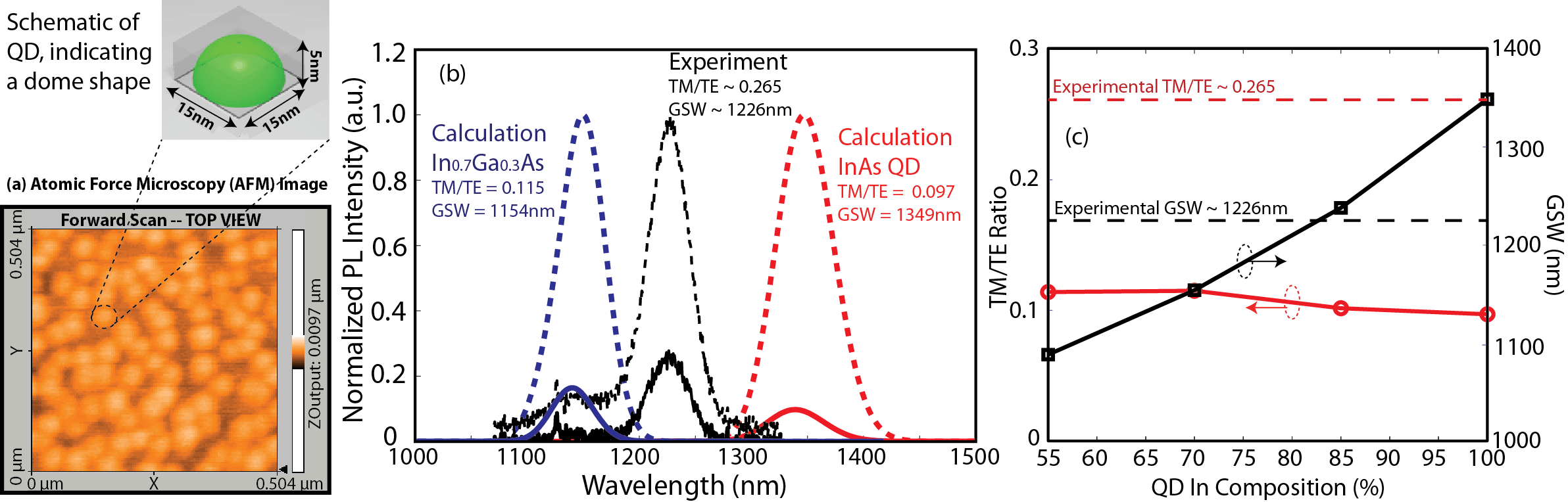
Experimental procedure: The QD samples used in this study were grown on semi-insulating GaAs substrates, by a COMPACT 21- Riber Molecular Beam Epitaxy (MBE) system equipped with a reflection high energy electron diffraction (RHEED) gun to monitor the surface evolution in-situ during growth. After growth of a GaAs buffer layer at 600∘C, the substrate temperature was lowered down to 500∘C and QDs were formed by covering the buffer with 2.8 MLs of InAs. The 2D-3D growth mode transition is demonstrated by the RHEED pattern evolving from streaky-like to spot-like after deposition of 1.7 MLs of InAs. Afterwards, dots were immediately capped by a GaAs spacer layer grown at the same low temperature. The single layer QD sample was then covered with a 20 nm GaAs cap terminating the structure. An uncapped single QD layer sample was also grown under the same conditions and its morphology analysed by atomic force microscopy (AFM), providing a dot density of 3.5x10¹⁰ dots/cm2 with average height of 5nm, as shown in Figure 1(a). The GaAs capped QDs were estimated by transmission electron microscopy (TEM) to have a dome-like shape with base diameter 15nm and height 5nm (see inset above Fig. 1(a)).
For investigating the polarization behavior, samples were excited from the top with a cw Ar+ laser ( = 514 nm). The room temperature photoluminescence (PL) signal from the cleaved edge of the samples was first collected by a long focal lens (200 mm) and it was then filtered by a linear polarizer and focused by a second lens into the monochromator.
Theoretical model: The theoretical modeling is performed using NEMO 3-DKlimeck_1 ; Klimeck_2 . NEMO 3-D is an atomistic simulator based on the valence force field (VFF) methodKeating_1 for strain calculations and the twenty band tight binding modelBoykin_1 for the electronic structure. NEMO 3-D is a multi-scale simulator capable of performing multi-million atom simulations for realistic QD dimensions surrounded by large GaAs buffers to model the long range impact of the strain and piezoelectric potential. This tool has already been used to model QD structures providing results in good agreement with experimental dataUsman_1 ; Usman_2 ; Usman_3 ; Usman_4 ; Lee_1 . Piezoelectric potentials, both linear and quadratic, are calculated by solving Poison’s equation according to a published recipeUsman_4 and are included in the calculations of the electronic spectra. The inter-band optical transition strengths are calculated using Fermi’s golden rule, with the squared magnitude of the optical matrix elements found by summing over the spin degenerate states. The polarization dependent TE and TM spectra are calculated along the [100] and [001] directions respectively, as a cumulative sum of optical transitions between the lowest conduction band energy level (E1) and the highest four valence band energy levels (H1, H2, H3, and H4), where each transition strength is artificially broadened by multiplication with a Gaussian distribution centered at the wavelength of the transitionUsman_1 . The highest four hole energy levels are chosen here instead of only the top most level (H1), because the valence band states are closely spaced on the energy scale (H1-H4 kT 26meV at T=300K) and multiple hole states contribute to the ground state optical emission peak at the room temperatureUsman_2 .
Model 1: uniform compositions: We start our analysis by first assuming a uniform material profile throughout the QD geometry as in previous theoretical studies of the polarization responseUsman_1 ; Saito_1 ; Usman_2 ; Sheng_1 ; Sheng_2 ; Williamson_1 . Dots are assumed to be lens-shaped with base diameter and height set at 15nm and 5nm, respectively, in accordance with the experimental TEM analysisRaino_1 . Figure 1(b) plots the experimental normalized PL spectra taken under the two polarization conditions (TE and TM) and compares them with the theoretically calculated spectra for both the ideal case of a pure InAs QD and an In0.7Ga0.3As random alloy QD. The InGaAs alloy configuration has been suggested by some previous theoretical studiesSheng_1 ; Sheng_2 ; Williamson_1 to mimic the In-Ga intermixing effect.
The pure InAs QD model clearly fails to reproduce the experimentally measured spectra. The TM/TE ratio is calculated to be 0.097 which is significantly lower than the experimentally measured value of 0.265. The peak wavelength in the PL spectra, hereafter referred to as ground state wavelength (GSW), is also overestimated by 123nm. This is consistent with the earlier theoretical studiesUsman_1 ; Saito_1 ; Sheng_1 where a pure-InAs-QD type model predicted TE-dominant optical emissions and failed to match the experimentally measured PL spectra. Lowering the average In composition inside the QD to 70 to mimic the effect of In-Ga intermixing during the capping process increases the TM/TE ratio to 0.115 due to the reduced biaxial strain, but at the same time blue shifts the GSW by 72nm with respect to the experimental value of 1226nm. To further investigate the impact of lowering the In composition of the QD, we gradually reduce its value from 100 (pure InAs QD) to 55 (In0.55Ga0.45As QD) and plot the corresponding values of the GSW and TM/TE ratio in Figure 1(c). As the In composition reduces, the GSW decreases to 1088nm, crossing the experimental value (shown by the dotted line) for In 84. However, the TM/TE ratio increases very slowly, only reaching a value of 0.114 for In=55. This clearly indicates that an uniform In-composition, either as pure InAs or some InGaAs alloy composition, cannot be selected as the chemical composition of the QD when seeking agreement between theory and experiment for both the GSW and TM/TE ratio. Therefore, a more complex compositional model is required in order to understand the experimental results.
Several experimentalBiasoil_1 ; Lemaitre_1 ; Passow_1 ; He_1 ; Chung_1 ; Goldman_1 ; Lita_1 and theoreticalShumway_1 ; Medhekar_1 ; Migliorato_1 ; Migliorato_2 ; Yang_1 studies have shown that In-Ga intermixing and In-segregation effects significantly influence the chemical composition of QDs during the growth of the GaAs capping layer. Thus we hypothesize that a quantitative agreement between theory and experiment can be achieved if some inter-diffusion of Ga atoms inside the QD region is included in the model. The most widely suggested profileBiasoil_1 ; Lemaitre_1 ; Passow_1 ; He_1 ; Chung_1 consists of an In-rich region along the vertical direction and a decreasing In-composition laterally from the center to the border. Such a complex configuration can be theoretically approximated by defining two composition regions inside the QD: an In-rich core surrounded by a low In-concentration region. Following these considerations, we now analyse the polarization response of such a QD model and explore the structural parameters to reproduce the experimental measurements.
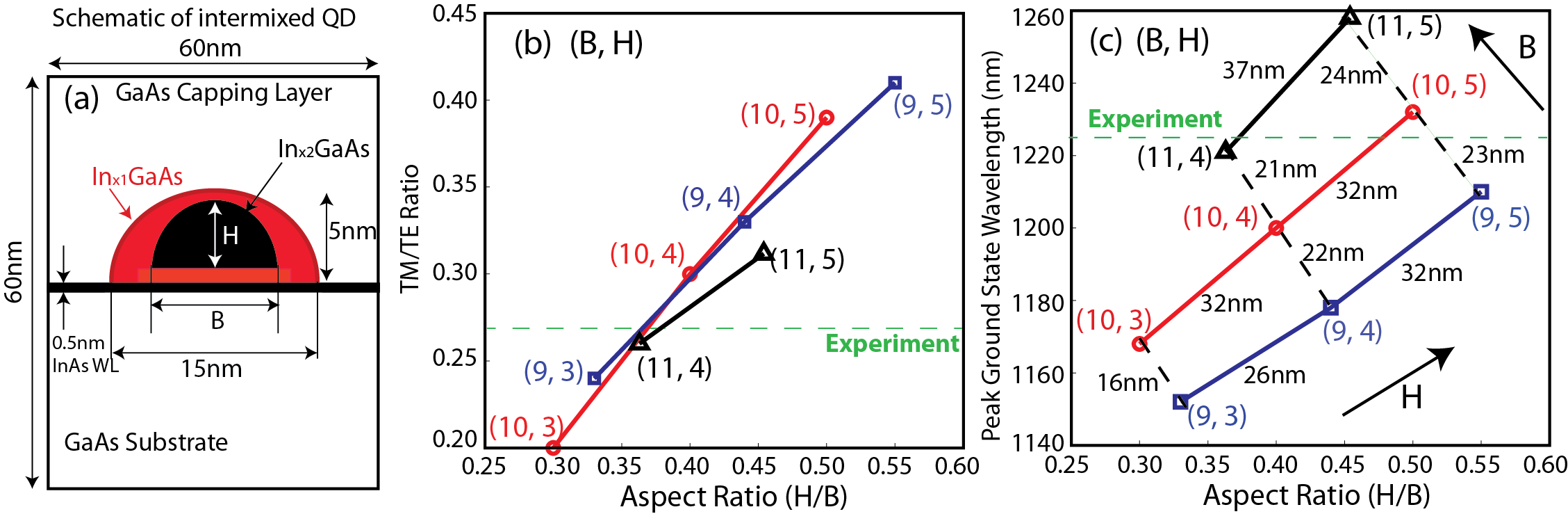
Model 2: non-uniform composition: In order to get the most reliable configuration, as close as possible to the experimental oneBiasoil_1 a simplified double region scheme is adopted, consisting of an In-rich inner core of Inx2Ga1-x2As (x2 typically 80) material, surrounded by an In-poor thin region of Inx1Ga1-x1As (x1 typically 40), as schematically shown in Figure 2(a). These ranges for the compositions x1 and x2 have been chosen from previous experimental resultsLemaitre_1 ; Passow_1 . The actual size of the In-rich core, defined by inner region base width (B) and height (H) as shown in Figure 2(a), strongly depends on the growth dynamics of the capping layer. The overall size of QD obtained from TEMRaino_1 places constraints on the values of B and H: H 5nm and B 15nm. On the basis of this QD model, we perform a systematic investigation by changing the parameters B, H, x1, and x2 and comparing the corresponding GSW, TE, and TM modes with the experimental measurements. Finally, it is worth noting that the two cases studied earlier in the uniform composition model, an InAs QD and an In0.7Ga0.3As QD, can be included by this two composition model by assuming x1=x2=100 and x1=x2=70, respectively.
Variations of B and H: First, in order to investigate the impact of the parameters H and B on the polarization response, we choose x2=100 and x1=40. Such an assumption is motivated by considering that the central core of InAs nano-islands is always reported as being In-rich and that the investigations reported so far indicate that the maximum value for the In-composition can reach 100Biasoil_1 .
Figures 2(b) and 2(c) plot the TM/TE ratio and the GSW, respectively, as a function of the aspect ratio (AR = H/B) of the inner core. The target experimental values are shown as horizontal dotted lines. The TM/TE ratio in Figure 2(b) linearly increases with AR when H is increased for a fixed value of B. This is because an increase in H will result in a reduction of the biaxial strain close to the center of the QD which will reduce the splitting between the HH and LH bands. As a result, the magnitude of the TM-mode will increase, thus increasing the TM/TE ratio. However, our calculations show that the slope of the TM/TE ratio as a function of AR=H/B is different for different values of B. In general, it decreases as B increases, indicating a decreasing impact of H on the TM/TE ratio. This is consistent with a previous theoretical studySchliwa_1 where hole energy levels in smaller QDs were found to be more sensitive to changes in QD AR as compared to larger QDs. We want to highlight here that our theoretical calculations show that even changes of 1-2nm in B or H values, which can actually be induced by highly controlled growth dynamics, result in a drastic change in the polarization properties of the QD sample.
The plots of GSW as a function of AR in Figure 2(c) exhibit a linear dependence of GSW on H for a fixed value of the B (shown by the solid lines), as well as a linear dependence of the GSW on the value of B for a fixed value of H (shown by the dotted lines). The analysis of Figure 2(b) and (c) indicates that two sets of values for (B, H), namely (10nm, 4nm) and (11nm, 4nm), give transition wavelengths and a TM/TE ratio close to the experimental values. A slight change in the sets of values of B and H ((10nm, 5nm) and (9nm, 5nm)) leads to a GSW value close to the experimental one, but introduces a discrepancy in the corresponding TM/TE ratios. We therefore choose (B, H) to be (10nm, 4nm) and (11nm, 4nm) to analyse in the following sections the impact that varying x1 and x2 has on the calculated values of the GSW and TM/TE ratio.
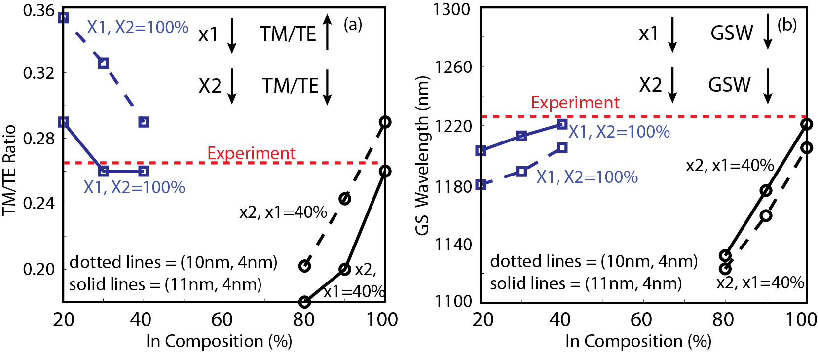
Variation in x1: The outer shell composition x1 was assumed above to be 40 in the study of the effect of the B and H parameters on the QD optical properties. However, this composition can have a lower value depending upon the growth dynamics during the growth of the GaAs capping layer. We therefore decrease this composition to 30 and 20 for both (10nm, 4nm) and (11nm, 4nm) dimensions, while keeping x2 at 100. Figures 3(a) and 3(b) show the impact of such variations in x1 on the TM/TE ratio and GSW, respectively. It is clear that decreasing the value of x1 has opposite impact on the TM/TE ratio and GSW: the value of TM/TE ratio increases and the value of the GSW decreases. Following these trends for the dimensions (B, H) plotted in Figures 2(b) and 2(c), we deduce that a decreasing GSW with respect to x1 will only bring (11nm, 5nm) and (10nm, 5nm) closer to the experimental GSW. However, the TM/TE ratio for these two dimensions is already higher than the experimental value (see Figure 2(b)), so a corresponding increase in the TM/TE ratio will further reduce their agreement with the experimental TM/TE ratio. Therefore, we deduce that decreasing x1 below 40 reduces agreement with the experimental values (either GSW or TM/TE ratio) for all of the dimensions (B, H) and hence we require the poor In-composition region comprising QD outer shell to have a composition close to 40.
Variation in x2: Next, we analyse the impact of the last unknown parameter x2 in our proposed two compositional model (see Figure 2(a)), keeping x1=40. Figures 3(b) and 3(c) plots variations in the TM/TE ratio and GSW, respectively, when x2 is decreased from 100 to 90 and 80. Contrary to x1, a decrease in x2 has similar impact on both the TM/TE ratio and GSW: both decrease as the composition x2 decreases. From Figures 2(b, c), these trends imply that the values of both the TM/TE ratio and GSW will become closer to the experimental values only for the two dimensions, (11nm, 5nm) and (10nm, 5nm). However, the GSW for the dimensions (10nm, 5nm) is very close to the experimental GSW whereas the TM/TE ratio for this dimension is significantly different from the experimental value. Hence a collective agreement of both the GSW and TM/TE ratio with the experimental values is not possible for a decrease in x2. For example, at x2=90, the GSW decreases to 1187nm (34nm below the experiment value) whereas the TM/TE ratio is still 0.31 (0.045 above the experimental value). For the (B, H) = (11nm, 5nm) case, if x2 decreases to 90, the GSW and TM/TE ratio decrease to 1208nm and 0.27, respectively, which are in reasonable agreement with the corresponding experimental values of 1221nm and 0.265.
We complete our analysis of QD compositions by considering simultaneous decrease in x1 and x2 and finding that their cumulative impact on the GSW and TM/TE values is roughly equal to the sum of their individual effects. We find that the TM/TE ratio is more sensitive to x2 as compared to x1, and therefore any simultaneous decrease in the compositions x1 and x2 will reduce the values of both parameters (GSW and TM/TE ratio).
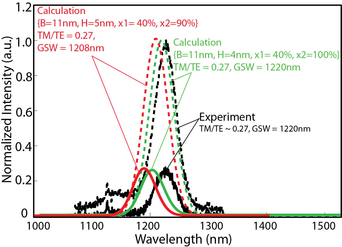
QD structural parameters: From the preceding discussions on the effect of B, H, x1, and x2 in the QD structure of the Figure 2(a), we conclude that for our experimentally measured QD sample, the most effective model is represented by the following parameters: B 11nm, H 4-5nm, x1 40, and x2 90-100 . The calculated PL spectra for based on these sets of parameters are compared with the experimental PL spectra in Figure 4. It is worth noting that the proposed structures roughly reproduce the complex composition profile experimentally found by many authorsBiasoil_1 , including the anisotropic In-Ga intermixing behavior with respect to the crystallographic direction, with a larger in-plane inter-diffusion region (nearly 2nm around the base of the dot) and a negligible inter-diffusion at the top (0-1nm) where segregation predominated.
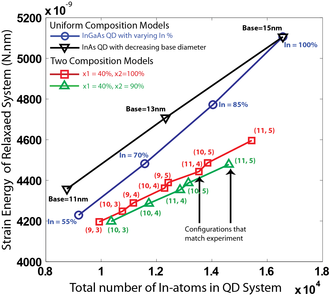
Relaxed strain energies: The QD systems have been relaxed using the VFF model to reach a minimum strain energy configurationKlimeck_1 ; Keating_1 . The comparison of the relaxed strain energies for the various QD systems under study may provide additional insight to find a more likely experimental geometry. Figure 5 plots the relaxed strain energies as a function of the total number of In-atoms for the various configurations after the VFF minimization is achieved. We consider two cases of the uniform composition model: an InxGa1-xAs QD with decreasing In-composition (see Figure 1(c)) and a pure InAs QD with decreasing base diameter. We also consider two cases of the non-uniform composition model: (B, H, x1=40, x2=100) and (B, H, x1=40, x2=90). Clearly, the relaxed strain energies belonging to the two layer composition configurations are lower than the strain energies of the uniform composition configurations for a similar number of In atoms. This suggests that a two composition model is more favourable as a proposed experimental geometry when compared to a uniform composition model, in accordance with our earlier findings.
Strain profile analysis: Our model 2 agrees with the experimental TE and TM PL spectra. However a comparison of strain profiles is required to further understand the difference between the calculated PL spectra for models 1 and 2. In Figures 6(a-c), we compare three QD configurations: (i) a pure InAs QD with base=15nm and height=5nm, (ii) an In0.7Ga0.3As alloy QD of the same size, and (iii) a two-layer composition as in Figure 2(a) with B=11nm, H=4nm, x1=40, and x2=100 which gives the best agreement with experiment. For reference, the previously calculated values of the GSW and TM/TE ratio are also listed underneath. To understand the shifts in the values of the TM/TE ratio and GSW in (b) and (c) with respect to (a), we compare the hydrostatic and biaxial strain plots along the [001] direction through the center of the QDs in Figures 6(d) and (e), respectively. For the In0.7Ga0.3As alloy QD, the strain values inside the QD region are randomly distributed due to the disordered composition of the alloy. We mark the average values of the hydrostatic and biaxial strains by the dotted horizontal lines.
The hydrostatic strain shifts the conduction and valence band edges, therefore increasing the band gap, whereas the biaxial strain is mainly responsible for controlling the splitting between the HH and LH valence band edgesUsman_3 . The strain driven band edge shifts in Table 1 are calculated from simple analytical expressions involving InAs/GaAs deformation potentialsUsman_3 .
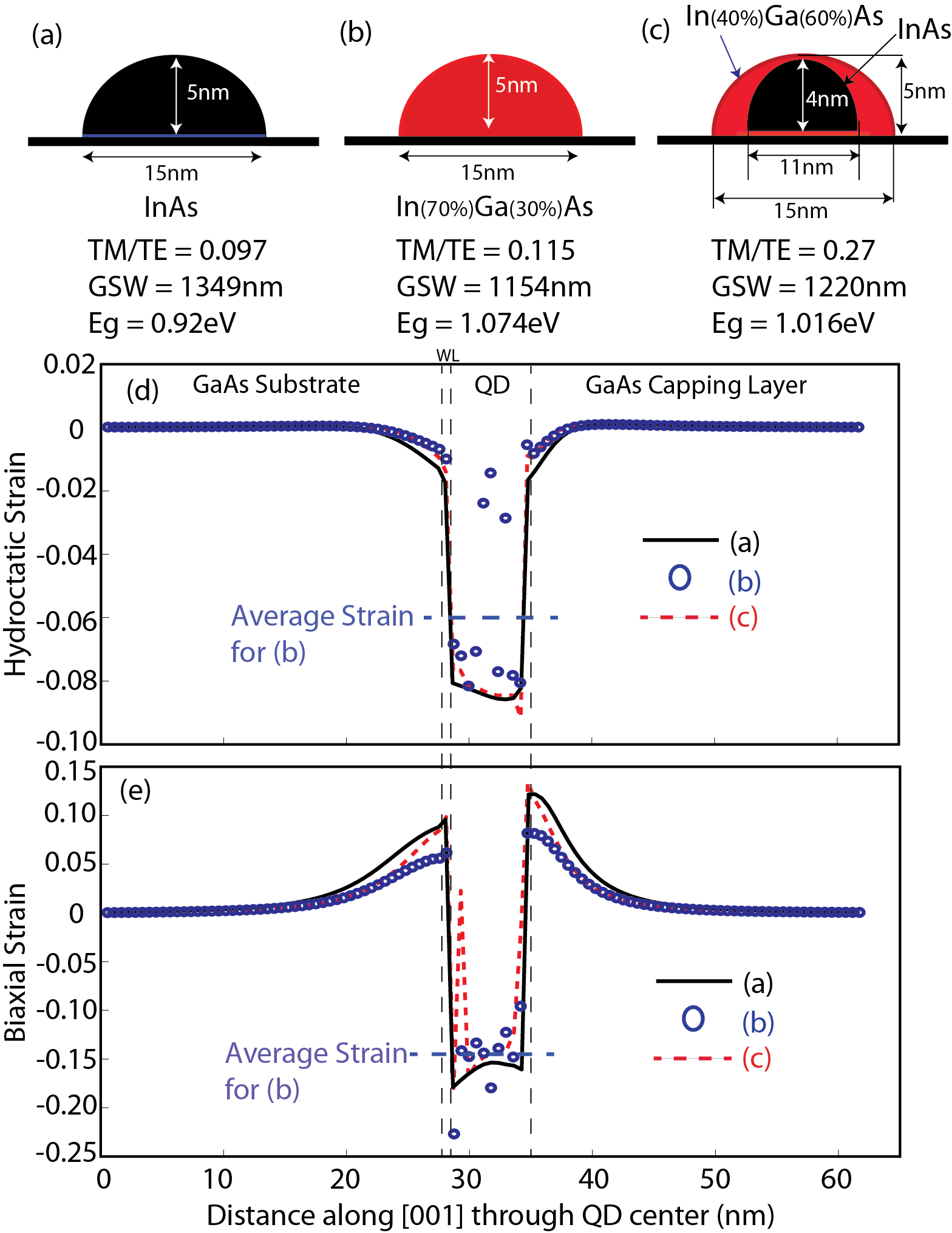
Blue shift of the GSW: The blue shifts in the GSW for (b) and (c) with respect to (a) indicate increase of the optical gaps (Eg), which can be understood as a cumulative affect of the relaxed hydrostatic strains and the increase of the band gaps due to the reduced average In compositions of the QDs Williamson_1 . By comparing the hydrostatic strain profiles in Figure 6 (d), we deduce that the presence of InGaAs alloy, in general, relaxes the strain which can be attributed to reduced QD lattice mismatch with the GaAs buffer. As a result, the band gaps for (b) and (c) will be smaller when compared to (a) due to smaller strain driven shifts in the conduction and heavy hole band edges. For example, from Table 1, the strain driven shifts predict that the band gap for the In0.7Ga0.3As QD is 373.7-231.6=142.1meV smaller than the InAs QD. However if the relative increase (310meV) in the band gap of the In0.7Ga0.3As QD due to the reduced average In composition is also added, the cumulative change is 310-142.1=167.9meV increase with respect to the InAs QD, consistent with the increase of the optical gap. To summarize, the relaxation of the hydrostatic strain due to presence of the InGaAs alloy in (b) and (c) introduces reductions in the band gaps which are smaller than the corresponding band gap increase due to the reduced average In compositions, and hence the cumulative impact of these two affects results in overall increase of the optical/band gaps (blue shifts of the GSWs) for (b) and (c) with respect to (a).
| QD | ECB | EHH | ELH | Egs | EH | ||
|---|---|---|---|---|---|---|---|
| Model | meV | meV | meV | meV | meV | ||
| (a) | -0.0842 | -0.1536 | 427.7 | 54 | -222.4 | 373.7 | 278.4 |
| (b) | -0.06 | -0.148 | 304.8 | 73.2 | -193.2 | 231.6 | 266.4 |
| (c) | -0.0818 | -0.1449 | 415.5 | 48.6 | -212.2 | 366.9 | 260.8 |
Biaxial strain relaxation increases TM/TE Ratio: Figure 6(e) compares the biaxial strain components and Table 1 provides the values of the corresponding changes in the HH and LH band edges for the three QD configurations. When compared to the pure InAs QD, the biaxial strain component is reduced for both the InGaAs alloy QD and the 2-composition QD model. This reduces the splitting between the HH and LH bands, thus increasing the LH component in the top most valence band states. A past theoretical investigationNarvaez_1 has also reported an increased HH/LH intermixing for an InGaAs QD when compared to a pure InAs QD. The increased LH character in turn enhances the TM componentUsman_1 , as we compute for configurations (b) and (c). The smallest HH/LH splitting responsible for the enhanced TM component occurs for the two-layer composition model.
Conclusions: In conclusion, multi-million atom simulations are performed to understand the correlation between the chemical composition of self-assembled QDs and their electronic properties by reproducing the experimentally measured polarization properties. A single composition QD model, being either a pure InAs QD or an alloyed InGaAs QD, failed to reproduce the experiment. To fully understand the experimental polarization behavior, the model must take In-Ga intermixing effects into account, by representing the QDs with variable compositions. Based on a systematic analysis of the dependence of the TM/TE ratio on the various QD morphology parameters, we propose a two composition model that accurately reproduces the measured PL response. The model gives results consistent with the experimental compositional findings and highlights the strong anisotropy of atomic scale phenomena like intermixing and segregation affecting the polarization behavior of these nanostructures. These results could represent a tool for using growth dynamics to engineer the strain field inside and around the QD structures, allowing tuning of the polarization properties, a critical parameter for several challenging applications.
Acknowledgements: Computational resources from National Science Foundation (NSF) funded Network for Computational Nanotechnology (NCN) through http://nanohub.org and Rosen Center for Advanced Computing(RCAC), Purdue University are acknowledged. MU and EPOR acknowledge financial support from European Union project BIANCHO (FP7-257974) and from Science Foundation Ireland (SFI).
References
- (1) A. Salhi et al., IEEE Journal of Selected Topics in Quantum Electronics, Vol. 14, No. 4, pp. 1188-1196, (2008).
- (2) T. Akiyama et al., proceedings of the IEEE, Vol. 95, No. 9, pp. 1757-1766, (2007).
- (3) A. Dousse et al., Nature, Vol. 466, Pages: 217-220, (2010).
- (4) M. Usman, T. Inoue, Y. Harda, G. Klimeck, and T. Kita, Physical Review B 84, 115321(2011).
- (5) M. Usman, S. Heck, E. Clarke, H. Ryu, R. Murray, and G. Klimeck, J. of Applied Physics 109, 104510 (2011).
- (6) L. Fortunato et al., Superlattices Microstruct. 47, 72 (2010).
- (7) H. Saito et al., Appl. Phys. Lett. 71, 590, (1997).
- (8) G. Visimberga et al., Appl. Phys. Lett. 93, 151112, (2008).
- (9) A. Mohan et al., Nature Photonics 4, 302 - 306 (2010).
- (10) T. Saito et al., Physical Review B 77, 195318 (2008).
- (11) T. Inoue et al., Applied Physics Letters 96, 211906 (2010).
- (12) D. Alonso-Álvarez et al., Advanced Materials, (2011), doi: 10.1002/adma.201101639.
- (13) Villegas-Lelovsky et al. Nanoscale Res. Lett. 6, 56, (2011).
- (14) A. V. Koudinov et al., Phys. Rev. B 70, 241305(R),(2004).
- (15) S. Shumway et al., Physical Review B 64, 125302 (2001).
- (16) N.V. Medhekar et al., Physical Review Lett. 100, 106104, (2008).
- (17) P.W. Fry et al., Phys. Rev. Lett. 84, 733 (2000).
- (18) J.A. Barker and Eoin P. O’Reilly, Physical Review B 61, 13840 (2000).
- (19) N. Liu, J. Tersoff, O. Baklenov, A.L. Holmes Jr., C.K. Shih, Phys. Rev. Lett. 84, 334 (2000).
- (20) L. Kegel et al., Physical Review Letters 85, 1694, (2000)
- (21) A. Limaitre et al., Appl. Phys. Lett. 85, 3717 (2004).
- (22) G. Biasoil and S. Heun, Physics Reports 500 (2011) 117-173.
- (23) W. Sheng and J.-P. Leburton, Appl. Phys. Lett. 80, 2755 (2002).
- (24) G. Klimeck et al., IEEE Trans. Elect. Devices 54, 2079 (2007).
- (25) G. Klimeck et al., IEEE Trans. Elect. Devices 54, 2090 (2007).
- (26) P.N. Keating, Physical Review 145, 637 (1966).
- (27) T. Boykin et al., Physical Review B 66, 125207 (2004).
- (28) S. Lee et al, Physical Review B 70, 125307, (2004).
- (29) M. Usman, H. Ryu, I. Woo, D.S. Ebert, and G. Klimeck, IEEE Trans. Nanotechnology, Vol. 8, No.3, Pages: 330-344, (2009).
- (30) M. Usman et al., Nanotechnology 22, 315709 (2011).
- (31) W. Sheng, Phys. Stat. Solidi B 246, No. 4, (2009).
- (32) A. J. Williamson et al., Physical Review B 62, 12963 (2000).
- (33) G. Raino et al., J. of Applied Physics 103, 096107 (2008).
- (34) T. Passow et al., J. Applied Phys. 102, 073511 (2007).
- (35) J. He et al., Nanotechnology 21, 255705 (2010).
- (36) H.-C. Chung et al., Applied Physics Lett. 92, 051903 (2008).
- (37) A.V. Semichaevsky et al., JOM, Vol. 63, No. 9, Pages: 20-26 (2011).
- (38) B. Lita et al., Applied Physics Lett. 75, 4082, (1999).
- (39) M.A. Migliorato, A.G. Cullis, M. Fearn, J.H. Jefferson, Phys. Rev. B 65 (2002) 115316.
- (40) G. A. Narvaez et al., J. Appl. Physics 98, 043708 (2005).
- (41) M. Yang, S.J. Xu, J. Wang, Appl. Phys. Lett. 92 (2008) 083112.
- (42) M.A. Migliorato, D. Powell, E.A. Zibik, L.R. Wilson, M. Fearn, J.H. Jefferson, M.J. Steer, M. Hopkinson, A.G. Cullis, Physica E 26 (2005) 436.
- (43) A. Schliwa et al., Physical Review B 76, 205324, (2007).