Band gaps in graphene via periodic electrostatic gating
Abstract
Much attention has been focused on ways of rendering graphene semiconducting. We study periodically gated graphene in a tight-binding model and find that, contrary to predictions based on the Dirac equation, it is possible to open a band gap at the Fermi level using electrostatic gating of graphene. However, comparing to other methods of periodically modulating graphene, namely perforated graphene structures, we find that the resulting band gap is significantly smaller. We discuss the intricate dependence of the band gap on the magnitude of the gate potential as well as the exact geometry of the edge of the gate region. The role of the overlap of the eigenstates with the gate region is elucidated. Considering more realistic gate potentials, we find that introducing smoothing in the potential distribution, even over a range of little more than a single carbon atom, reduces the attainable band gap significantly.
pacs:
73,22.Pr, 73.21.CdI Introduction
While grapheneNovoselov et al. (2004) has proven to be a remarkable material, with electronic properties that are interesting from a fundamentalCastro Neto et al. (2009); Novoselov et al. (2005) as well as a technological viewpoint,Geim and Novoselov (2007); Geim (2009) the absence of a band gap severely limits its possible applications. Several methods have been proposed for opening a gap in graphene. Relying on quantum confinement effects, the most immediate way of making graphene semiconducting is by reducing the dimensionality by cutting graphene into narrow ribbons. Such so-called graphene nanoribbons (GNRs) have band gaps that in general scale inversely with the width of the GNR, but which are very sensitive to the exact geometry of the edge of the ribbon.Nakada et al. (1996); Brey and Fertig (2006); Son et al. (2006) Related to these ideas, periodically perforated graphene, termed graphene antidot lattices, effectively result in a network of ribbons, and has been shown to be an efficient way of inducing an appreciable band gap in graphene. Pedersen et al. (2008a) This idea has been successfully applied to fabricate simple graphene-based semiconductor devices.Bai et al. (2010); Kim et al. (2010) Modifying graphene via adsorption of hydrogen presents another route towards opening a gap in graphene, with fully hydrogenated graphene exhibiting a band gap of several electron volts,Sofo et al. (2007); Elias et al. (2009) while patterned hydrogen adsorption yields band structures resembling those of graphene antidot lattices, with reported band gaps of at least meV.Balog et al. (2010)
The prospect of opening a band gap in graphene via electrostatic gating is intriguing, since it would allow for switching between semi-metallic and semiconducting behavior and to dynamically alter the band gap to fit specific applications. This makes it significantly more flexible than proposals relying on structural modification of graphene. However, a linearization of the tight-binding Hamiltonian of graphene, resulting in the now widely studied Dirac equation (DE) of graphene,Semenoff (1984); Castro Neto et al. (2009) suggests that the Dirac fermions of graphene cannot be confined by electrostatic gating, due to the phenomenon of Klein tunneling.Katsnelson et al. (2006); Beenakker (2008) Thus, while periodic gating of usual semiconductor heterostructures such as, e.g., GaAs quantum wells, does induce gaps in the dispersion relation,Pedersen et al. (2008b) previous theoretical studies have indicated that band gaps are induced for neither one-dimensional Barbier et al. (2008, 2009) nor two-dimensionalPark et al. (2008) periodic gating of graphene.
These studies have taken as their starting point the Dirac model of graphene, which is a low-energy continuum model, ignoring atomistic details. Here, we instead use a more accurate tight-binding (TB) model to study periodically gated graphene. Contrary to predictions of continuum (Dirac) models, the TB model suggests that it is indeed possible to open a band gap in graphene via periodic gating. The aim of this paper is two-fold: (i) To compare periodically gated graphene with graphene antidot lattices. In doing so we will illustrate that, contrary to what may be expected from the Dirac equation, a sufficiently large scalar potential, i.e., not necessarily a mass term, yields a band structure that is highly similar to that of perforated graphene structures; (ii) to serve as a feasibility study of periodic gating as a means of inducing a band gap in graphene. To this end, we will illustrate and discuss the non-trivial dependence of the band gap on the gate potential, as well as the intricate relation between band gap and the edge geometry of the gated region. These results will also serve to illustrate some of the key differences between graphene and ordinary two-dimensional electron gases. While, initially, the potential will be modeled as a simple step function, we will show below that introducing smoothing in the potential distribution severely reduces the attainable band gap.
Continuum and atomistic models of periodically gated graphene have previously been compared in Ref. Zhang et al., 2010. That study, however, focused on a single value of the potential strength and only considered structures that are rotated compared to the ones of the present work and, therefore, do not necessarily display any band gap even for perforated structures.Petersen et al. (2011) Moreover, in this work we examine in detail the non-trivial dependence of the band gap on the magnitude of the potential and we consider more realistic, smooth potential profiles. Finally, we elucidate the intricate dependence on the precise edge geometry and show how the energy gap correlates with the gate region overlap of electron and hole states.
II Models

In Fig. 1 we illustrate the graphene structures that we will consider in this article. We consider only superlattices with triangular symmetry, as shown in the figure. An important decision lies in the choice of the angle between the basis vectors of the superlattice and the carbon-carbon bonds in graphene. In particular, if the superlattice basis vectors are rotated compared to the carbon-carbon bonds (such as in Ref. Zhang et al., 2010), Clar sextet theory predicts that perforated graphene structures only exhibit significant band gaps for every third value of the side length of the hexagonal unit cell.Petersen et al. (2011) In contrast to this, perforated graphene structures with basis vectors parallel to the carbon-carbon bonds always have band gaps. We choose to focus in this paper on the latter geometries, in order to ensure that the superlattice symmetry in itself does not prohibit the emergence of a band gap.
We characterize a given structure by , where denotes the side length of the hexagonal unit cell, while is the radius of the central region, both in units of the graphene lattice constant, as illustrated in Fig. 1. In these units, also corresponds to the number of benzene rings along each edge of the unit cell. Note that the exact geometry of the edge of the central region differs greatly depending on the radius . Below, we discuss in detail the crucial dependence of the results on the edge geometry. We will consider four distinct ways of periodically modifying graphene: (a) Perforated graphene (graphene antidot lattices), with carbon atoms removed from the central region, (b) a periodic mass term, non-zero only in the central region, and (c) periodically gated graphene, with a constant gate potential within the central region and a vanishing potential outside. Furthermore, to discuss the feasibility of realizing gapped graphene via periodic gating, we will also consider (d) periodically gated graphene, with a more realistic model of the spatial dependence of the gate potential, obtained from a solution to the Laplace equation. Focus will be on periodically gated graphene, with the other forms of modulation included for comparison only.
To illustrate the dependence of the results on the exact edge of the gate or mass region, we will use a Dirac model as well as a more accurate tight-binding treatment, in which the atomistic details of the structures are included. We find significant discrepancies between these two methods, quantitatively as well as qualitatively. In particular, we will show that the DE does not predict a band gap opening for periodic gating, which is present in the TB results. In what follows, we briefly describe the two models. In the continuum model of the problem, we employ the Dirac Hamiltonian
| (1) |
where m/s is the Fermi velocity, while denotes the gate potential or mass term. Here, the () is used when modeling a gate potential (mass term). Imposing periodic Bloch boundary conditions at the edge of the unit cell, we solve the problem in a plane-wave spinor basis, and , with the Bloch wave vector and the reciprocal lattice vectors. We take , with the Heaviside step function, yielding , where is the unit cell area while is the Bessel function of the first kind. A total of plane-wave spinors were included in the calculations, to ensure convergence of the results.
In the tight-binding model we include only nearest-neighbor coupling between orbitals, parametrized via the hopping term , with eV. We ignore the overlap between neighboring orbitals, assuming that our basis is orthogonal, and set the on-site energy of the orbitals to zero. This parametrization accurately reproduces the Fermi velocity of graphene, and is also in quantitative agreement with density functional theory when applied to perforated graphene structures.Fürst et al. (2009a) For periodically gated graphene, we set the diagonal terms of the Hamiltonian equal to the gate potential. In the case of a mass term, the diagonal terms become , with the sign depending on which sublattice the carbon atom resides on. For perforated graphene, atoms are removed entirely in the region of the hole, ensuring that no dangling bonds are created. While including next-nearest neighbor coupling, as well as taking into account the non-orthogonality of the basis set, will change our results quantitatively, we expect the overall trends and the conclusions to remain the same in more accurate models.
III Band structures
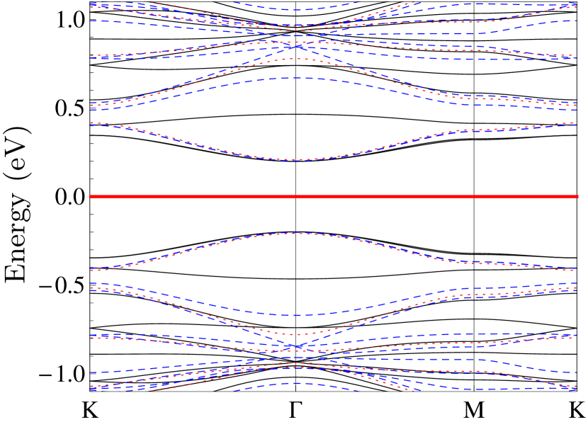
In Fig. 2 we show the band structure for a graphene antidot lattice, i.e., periodically perforated graphene, and compare to the case of a periodic mass term, modeled using either the TB or the DE approach. A sufficiently large mass term should ensure that electrons are excluded entirely from the region of the mass term, and we thus expect relatively good correspondence with perforated graphene. In the figure, we consider the case where the mass term is equal in size to the TB hopping term, . As expected, we find quite good agreement between all three methods. In particular, the magnitudes of the band gaps are in near-perfect agreement. Using a finite, but sufficiently large mass term in the DE model thus yields much better results than models where the limit of infinite mass term is used to impose boundary conditions on the edge of the hole in the DE model.Fürst et al. (2009a) Note that electron-hole symmetry is preserved for all models. For higher-lying bands, the differences between the DE and TB results become more pronounced, as the linear approximation of the DE model breaks down. Further, comparing the case of perforated graphene to that of a periodic mass term in the TB model, we see significant differences in the higher-lying bands. However, we note that increasing the mass term further results in excellent agreement with the perforated graphene case, for all bands shown.
A periodic mass term is expected to induce a gap in graphene due to the fact that it explicitly breaks sublattice symmetry via the operator in the continuum model or, similarly, through the staggered on-site potential in the TB approach. Contrary to this, analysis of periodic potentials in a DE model of graphene suggests that periodic gating does not induce a gap in graphene around the Fermi level,Barbier et al. (2008, 2009) but rather leads to the generation of new Dirac points near the superlattice Brillouin zone boundaries.Park et al. (2008) Superlattices lacking inversion symmetry have been suggested as a means of achieving tunable band gaps in graphene, based on results using a DE model.Tiwari and Stroud (2009) However, these results were recently found to be based on numerical errors.Tiwari and Stroud (2012) Indeed, based on the DE model, a gap cannot be produced by any Hamiltonian that preserves time-reversal symmetry, i.e. , where is the Pauli spin matrix while denotes the complex conjugate (not the Hermitian conjugate) of the Hamiltonian.Lin et al. (2012) A pure scalar potential, such as the one we consider for periodically gated graphene, see Eq. (1), preserves this symmetry and the DE model thus suggests that periodic gating does not open a band gap. Instead, a combination of a scalar as well as a vector potential is needed.Lin et al. (2012)
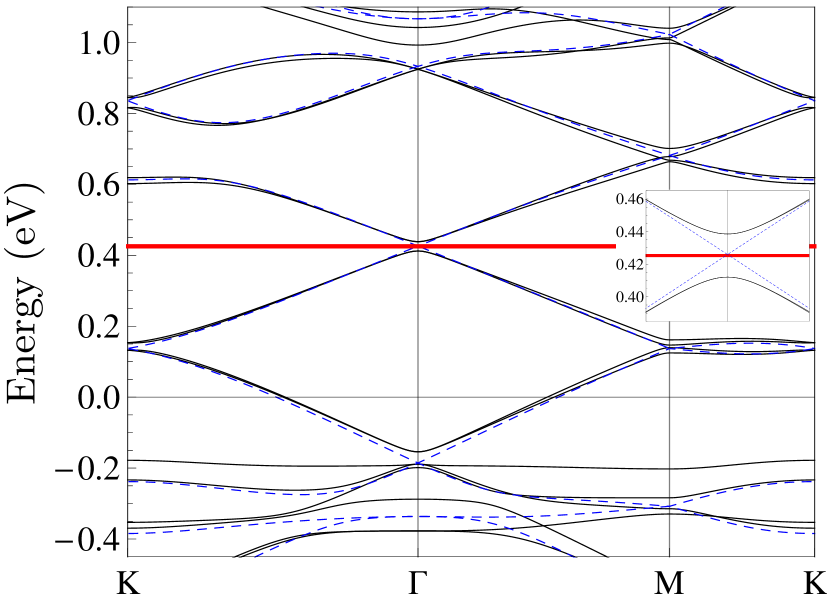
In Fig. 3 we show the band structure of a periodically gated graphene structure, with a gate potential of half the TB hopping term, . Results are shown for TB and DE models, respectively. Contrary to a periodic mass term we see that, as could be expected, periodic gating breaks electron-hole symmetry and shifts the Fermi level to higher energies. Comparing DE and TB results, we note that there is quite good agreement overall, between the two methods. However, a crucial difference emerges when considering the bands in close vicinity of the Fermi level, as illustrated in the inset: while the DE results suggest that periodic gating does not open a band gap, TB results demonstrate that a band gap does occur right at the Fermi level. We attribute this to a local sublattice symmetry breaking at the edge of the gate region and substantiate this claim below. We note that while a band gap appears, the magnitude of the band gap is of the order of tens of meV, an order of magnitude smaller than that of the corresponding perforated graphene structure. This dramatic qualitative difference between TB and DE modelling agrees with previous results Zhang et al. (2010) comparing density functional theory and Dirac models for rotated triangular geometries.
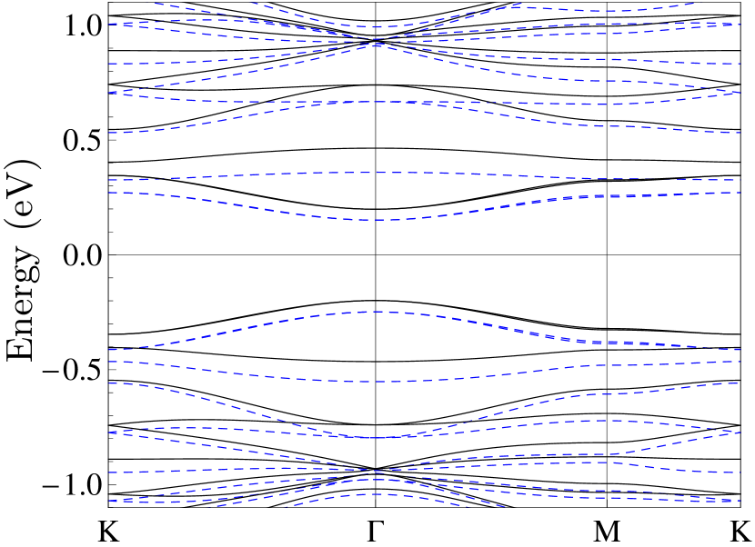
Above, we illustrated how a sufficiently large mass term serves as an excellent model of a hole in graphene, see Fig. 2. Because a simple scalar potential cannot confine Dirac electrons Katsnelson et al. (2006); Beenakker (2008), one would expect that modeling the hole via a large gate potential would be inaccurate. In Fig. 4 we show the band structure of periodically gated graphene, with a very large gate potential of .foot For comparison, we also show the corresponding perforated graphene structure. Contrary to the aforementioned expectations, we see that the periodically gated graphene structure is an excellent model of perforated graphene. We note that increasing the gate potential further results in near-perfect agreement between the periodically gated and the perforated structures. With a gate potential of we are way beyond the linear regime of the band structure, for which a Dirac treatment of graphene is viable, which explains why the theoretical arguments pertaining to Dirac electrons break down in this case.
III.1 Gate region overlap
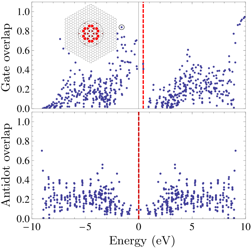
Returning now to the band structure for the periodically gated lattice, shown in Fig. 3, we note the appearance of a nearly dispersionless band near eV. This state is localized predominantly within the gate region. In the upper panel of Fig. 5 we show the overlap of all eigenstates with the gate region as a function of energy, calculated at the point. For comparison, we show the corresponding results for a periodic mass term in the lower panel. We note that several states exist, which have significant overlap with the gate region, also at energies below the Fermi level. An example of one such state is shown in the figure. As the gate potential is increased further, these states become less energetically favorable, and are eventually all situated at energies well above the Fermi level. In stark contrast to this, a periodic mass term dictates perfect electron-hole symmetry, and thus always predicts states below the Fermi level having significant overlap with the gate region. In fact, as the mass term is increased, states nearly entirely localized within the mass term region develop at both extrema of the spectrum. Below, we will illustrate how this fundamental difference between a mass term and a scalar potential manifests itself via the dependence of the band gap on the magnitude of the gate potential for periodically gated graphene.
IV Band gaps in periodically gated graphene
Having determined that a TB treatment of periodically gated graphene does indeed suggest the opening of a band gap at the Fermi level, we now proceed to investigate the behavior of the band gap magnitude in more detail. From hereon, all results shown have been calculated using the TB model.
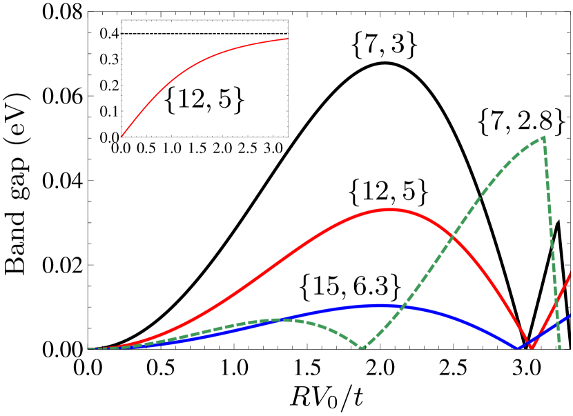
In Fig. 6, the solid lines show the magnitude of the band gap at the Fermi level for three different lattices, , , and , all of which have approximately the same ratio of gate radius to side length of the hexagonal unit cell. When plotted against the gate radius times the gate potential, the resulting curves emerge as simple scaled versions of each other, as seen in Fig. 6. While, initially, raising the gate potential increases the band gap, a maximum gap is reached at a certain gate potential, after which the band gap diminishes. This behavior is completely different from the case where the potential is replaced by a mass term, as illustrated in the inset of the figure. In this case, the band gap continues to increase until a saturation point is reached in the limit where the structure resembles that of perforated graphene. While the three periodic lattices indicated with solid lines in Fig. 6 result in similar dependencies of the gap on , we stress that this is not the case for all lattices, even if the ratio is approximately the same. To illustrate this, we also show in Fig. 6 results for the lattice. The dependence of the band gap on gate potential differs markedly for this lattice. This indicates that the exact geometry at the edge of the gate region plays a large role in determining the band gap, in agreement with findings in Ref. Zhang et al., 2010.
IV.1 Edge dependence
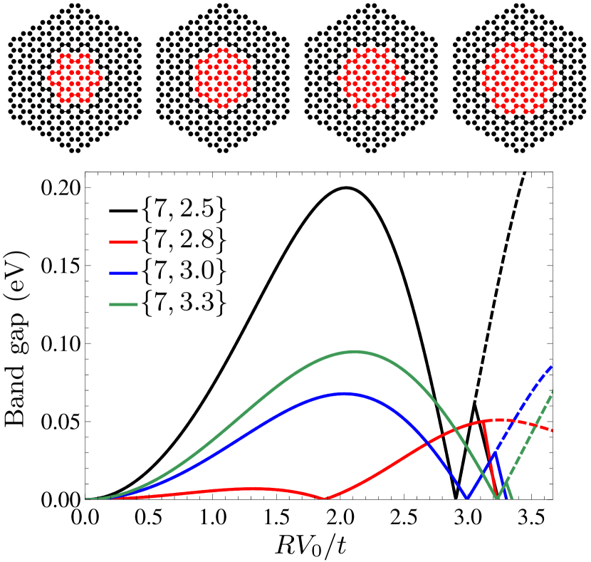
To illustrate in more detail the role of the edge in determining the band gap, we show in Fig. 7 the band gap as a function of the gate potential, for lattices with increasing values of . The radius is increased in the minimum steps resulting in new geometries. The structures with show quite similar behaviors. In particular, a maximum band gap is reached at in all three cases. The band gap then closes, but reopens once more as the gate potential is increased further. Around the band gap changes from direct (–) to indirect (–) as the gate voltage is raised. The dashed lines in the figure illustrate the – gap above the direct to indirect-gap transition. However, after a slight further increase of the gate voltage, the final closing of the band gap occurs as the energy at the point moves below that at the point, resulting in crossing bands at the Fermi level. Finally, we note that while the three lattices show similar behavior, the dependence of the band gap on the radius of the gate region is clearly not monotonic, and a larger gate region does not necessarily result in a larger band gap.
In contrast to the similarities of the other three structures, the dependence of the band gap on the gate potential for the lattice differs greatly. In the upper panel of Fig. 7 we show the unit cells corresponding to the lattices considered, with the edge geometries highlighted. The lattice stands out from the rest of the geometries, in that the entire edge of the gate region is made up from several pure zigzag edges. We stress that the sublattice imbalance for the entire edge is zero, while there is a local sublattice imbalance on the individual straight zigzag edges. In contrast to this, the other geometries have gate regions with zigzag as well as armchair edges. We find that the general trend is for zigzag edges to quench the band gap of the periodically gated graphene structures, which we have also verified via calculations of gate regions of hexagonal symmetry, which always have pure zigzag edges. This trend can be explained by noting that pure zigzag edges, such as, e.g., in zigzag graphene nanoribbons Nakada et al. (1996); Brey and Fertig (2006) or graphene antidot lattices with triangular holes Vanević et al. (2009); Fürst et al. (2009b); Gunst et al. (2011), lead to localized midgap states.Inui et al. (1994) For periodically gated graphene the edge is defined by a finite potential, rather than a complete absence of carbon atoms, so we expect the tendency of electrons to localize on the edge to be less pronounced. Nevertheless, our findings suggest that local zigzag geometry still has the effect of quenching the band gap. Since, in general, larger circular holes will have longer regions of zigzag geometry at the edge of the gate region, this explains why larger gate regions will not invariably lead to larger band gaps. In the present case, we note that the structure indeed has a significantly smaller band gap than the structure. The lattice is unique in that the equivalent of dangling bonds are present at the edge of the gate region, which further decrease the magnitude of the band gap.
IV.2 Dependence on gate region overlap
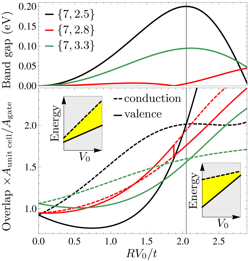
First-order perturbation theory suggests that the dependence of the energy of the eigenstate on the gate potential be proportional to the overlap of the state with the gate region, i.e., . We thus expect the overlap with the gate region of the two eigenstates closest to the Fermi level to be a crucial parameter in describing the opening and quenching of the band gap as the gate voltage is varied. We will also see that it illustrates the crucial differences between graphene and ordinary two-dimensional electron gases. In Fig. 8 we show the overlap of the eigenstate with the gate region as a function of the magnitude of the potential. The overlap is shown for the eigenstates at the valence and conduction band edges, and normalized by the ratio between gate and unit cell areas. A value of one thus indicates that the overlap with the gate region is the same as if the eigenstate is evenly distributed throughout the unit cell, while a value larger (smaller) than one suggests that the eigenstate is localized predominantly inside (outside) the gate region. As we saw also in Fig. 5, the states near the Fermi level both have quite large overlaps with the gate region, even when the potential is of the order of the TB hopping term. Initially, for low values of the gate potential, the overlap with the gate region of the unoccupied state in the conduction band is larger than the corresponding overlap of the occupied state in the valence band. Relying on first-order perturbation theory we thus expect the energy of the conductance band state to increase more strongly with the gate potential than the valence band state, resulting in a larger band gap as the gate potential is raised, as illustrated in the left inset of Fig. 8. However, contrary to what would be expected for an ordinary two-dimensional electron gas, we see that as the potential is increased further, the valence band state also becomes localized predominantly within the gate region. Indeed, eventually the overlap of the valence band state with the gate region becomes larger than the one of the conduction band state, which results in a quenching of the band gap as the potential is increased further, as illustrated in the right inset of Fig. 8. We note that the point where the overlap of the two states with the gate region become equal exactly matches the point where the band gap is at a maximum. This is illustrated by the vertical, black line in the figure. The strong influence of the exact edge geometry is apparent, manifesting itself in a qualitatively different dependence of the overlap on gate voltage for the lattice. In particular, while the gate region overlap of the valence band state of the and lattices initially decreases with the size of the potential, both valence and conduction band states immediately start localizing within the gate region for the structure. This leads to much faster quenching of the initial band gap.
IV.3 Realistic potential profiles
As we have illustrated above, the band gap of periodically gated graphene depends strongly on the edge geometry at the boundary between the gated and the non-gated region. So far, we have used a simple step function to model the spatial dependence of the potential due to the gate. However, it is obvious that in actual realizations of periodically gated graphene, some form of smoothing of the potential will inevitably be present. Due to the intricate relationship between the band gap and the edge geometry, it is relevant to investigate the effect of smoothing out the potential. In particular, since the DE model predicts no gap at all, one may wonder whether smoothing will cause the gap to close entirely. Previous studies have included smoothing of the gate potential, but with a smearing distance of the order Å,Zhang et al. (2010) small enough that an atomically resolved edge can still be defined.
To model a more realistic gate potential, we use an analytical expression for the potential distribution resulting from a constant potential disk in an insulating plane, obtained by direct solution of the Laplace equation. In cylindrical coordinates, this reads asNanis and Kesselman (1979)
| (2) |
with the distance above the gate, while is the distance from the center of the disk. Note that for the expression simplifies to for while for . Of course, more exact approaches such as, e.g., finite-element methods, could be used to determine the potential distribution from a realistic back gate. However, we choose to use this relatively simple analytical expression, since we are mainly interested in discussing the general trends that occur as the edge of the potential region becomes less well-defined. One could imagine more elaborate setups that would generate sharper potential distributions. To include such possibilities, we consider a modified potential distribution , with the additional parameter , which allows us to control the smoothing of the potential further. As we approach the limit where the potential is described by a Heaviside step function, as in the results presented so far. We note that Eq. (2) is derived for an isolated constant potential disk rather than a periodic array of gates. Ignoring coupling between the different gates, one simple way of improving this model would be to add the potentials generated from the nearest-neighbor gates, to account for the overlap between them. However, this would merely serve to smoothen out the potential further, as well as add a constant background potential, effectively decreasing the height of the potential barrier. Here, we are interested in illustrating the critical dependence of the band gap on smoothing out the potential, so we are adopting a ‘best case’ scenario, which also means that we will use throughout, assuming that the graphene layer is deposited directly on the periodic gates, with no insulating layer in-between.
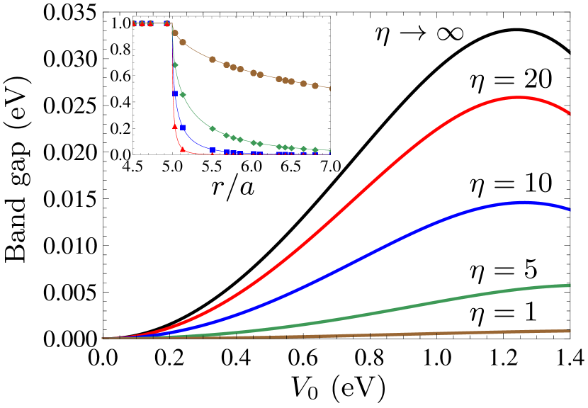
In Fig. 9 we show the band gap for a lattice as a function of gate potential, for increased values of the parameter. While for , corresponding to a Heaviside step function distribution, the maximum band gap is about meV, the band gap for is drastically lower, with a maximum value of only meV. As we artificially decrease the amount of smoothing by raising the value of , we slowly recover the maximum band gap attainable. However, we stress that even for , which as shown in the inset of the figure amounts to smoothing over a range of little more than a single carbon atom, the maximum band gap has decreased by more than 20% from the value at . This suggests that the band gap does indeed critically depend on an edge effect, which is very quickly washed out as the potential step is smoothed out over several carbon atoms. This is in agreement with previous studies, which have indicated that intervalley scattering is crucial in describing the band gap of periodically gated graphene.Zhang et al. (2010) In order for a scalar potential to induce intervalley scattering, it must vary significantly on a scale of the carbon-carbon distance, so that a local sublattice asymmetry is introduced.
V Summary
By employing a tight-binding description of graphene, we have shown that, contrary to what is predicted on basis of a continuum model, it is indeed possible to induce a band gap in graphene via periodic, electrostatic gating. Further, if the magnitude of the potential is made sufficiently large, periodically gated graphene is an accurate model for perforated graphene structures, with one caveat, namely that the Fermi level is far removed from the location of the band gap. For smaller, more realistic values of the gate potential, a band gap appears right at the Fermi level. However, we find that the band gap is orders of magnitude smaller than that of the corresponding perforated graphene structure.
The dependence of the band gap on the gate potential is highly non-trivial, and entirely different from the case where graphene is modulated by a periodic mass term. In particular, a maximum magnitude of the band gap is reached, after which increasing the gate potential further quenches the gap. Also, a transition from a direct (–) to an indirect (–) semiconductor occurs for larger gate potentials. The exact magnitude and dependence of the band gap on gate potential depends critically on the precise geometry of the edge of the gate region. In particular, large regions of local zigzag geometries tend to result in significantly smaller band gaps than geometries where armchair edges dominate.
Because the emergence of a band gap relies on a local sublattice asymmetry, we find that it is extremely fragile. If smoothing is introduced in the potential distribution, such that the edge of the gate region is no longer atomically resolved, the magnitude of the band gap drops significantly. Even if the smoothing occurs over a range of little more than a single carbon atom, we find that the maximum band gap decreases to less than 80% of the value for a perfectly defined edge. This presents a serious challenge to opening a band gap in graphene via periodic gating.
Acknowledgements.
The work by J.G.P. is financially supported by the Danish Council for Independent Research, FTP grant numbers 11-105204 and 11-120941. The Center for Nanostructured Graphene (CNG) is sponsored by the Danish National Research Foundation. We thank Prof. Antti-Pekka Jauho for helpful comments during the development of the manuscript.References
- Novoselov et al. (2004) K. S. Novoselov, A. K. Geim, S. V. Morozov, D. Jiang, Y. Zhang, S. V. Dubonos, I. V. Grigorieva, and A. A. Firsov, Science 306, 666 (2004).
- Castro Neto et al. (2009) A. H. Castro Neto, F. Guinea, N. M. R. Peres, K. S. Novoselov, and A. K. Geim, Rev. Mod. Phys. 81, 109 (2009).
- Novoselov et al. (2005) K. S. Novoselov, A. K. Geim, S. V. Morozov, D. Jiang, M. I. Katsnelson, I. V. Grigorieva, S. V. Dubonos, and A. A. Firsov, Nature 438, 197 (2005).
- Geim and Novoselov (2007) A. K. Geim and K. S. Novoselov, Nature Materials 6, 183 (2007).
- Geim (2009) A. K. Geim, Science 19, 1530 (2009).
- Nakada et al. (1996) K. Nakada, M. Fujita, G. Dresselhaus, and M. S. Dresselhaus, Phys. Rev. B 54, 17954 (1996).
- Brey and Fertig (2006) L. Brey and H. A. Fertig, Phys. Rev. B 73, 235411 (2006).
- Son et al. (2006) Y.-W. Son, M. L. Cohen, and S. G. Louie, Phys. Rev. Lett. 97, 216803 (2006).
- Pedersen et al. (2008a) T. G. Pedersen, C. Flindt, J. Pedersen, N. A. Mortensen, A.-P. Jauho, and K. Pedersen, Phys. Rev. Lett. 100, 136804 (2008a).
- Bai et al. (2010) J. Bai, X. Zhong, S. Jiang, Y. Huang, and X. Duan, Nature Nanotechnology 5, 190 (2010).
- Kim et al. (2010) M. Kim, N. S. Safron, E. Han, M. S. Arnold, and P. Gopalan, Nano Lett. 10, 1125 (2010).
- Sofo et al. (2007) J. O. Sofo, A. S. Chaudhari, and G. D. Barber, Physical Review B 75, 153401 (2007).
- Elias et al. (2009) D. C. Elias, R. R. Nair, T. M. G. Mohiuddin, S. V. Morozov, P. Blake, M. P. Halsall, A. C. Ferrari, D. W. Boukhvalov, M. I. Katsnelson, A. K. Geim, and K. S. Novoselov, Science 323, 610 (2009).
- Balog et al. (2010) R. Balog, B. Jørgensen, L. Nilsson, M. Andersen, E. Rienks, M. Bianchi, M. Fanetti, E. Lægsgaard, A. Baraldi, S. Lizzit, Z. Sljivancanin, F. Besenbacher, B. Hammer, T. G. Pedersen, P. Hofmann, and L. Hornekær, Nature Materials 9, 315 (2010).
- Semenoff (1984) G. W. Semenoff, Phys. Rev. Lett. 53, 2449 (1984).
- Katsnelson et al. (2006) M. I. Katsnelson, K. S. Novoselov, and A. K. Geim, Nat. Phys. 2, 620 (2006).
- Beenakker (2008) C. W. J. Beenakker, Rev. Mod. Phys. 80, 1337 (2008).
- Pedersen et al. (2008b) J. Pedersen, C. Flindt, N. A. Mortensen, and A.-P. Jauho, Phys. Rev. B 77, 045325 (2008b).
- Barbier et al. (2008) M. Barbier, F. M. Peeters, P. Vasilopoulos, and J. M. Pereita, Phys. Rev. B 77, 115446 (2008).
- Barbier et al. (2009) M. Barbier, P. Vasilopoulos, and F. M. Peeters, Phys. Rev. B 80, 205415 (2009).
- Park et al. (2008) C.-H. Park, L. Yang, Y.-W. Son, M. Cohen, and S. G. Louie Phys. Rev. Lett. 101, 126804 (2008).
- Zhang et al. (2010) A. Zhang, Z. Dai, L. Shi, Y. P. Feng, and C. Zhang, J. Chem. Phys. 133, 224705 (2010).
- Petersen et al. (2011) R. Petersen, T. G. Pedersen, and A.-P. Jauho, ACS Nano 5, 523 (2011).
- Fürst et al. (2009a) J. A. Fürst, J. G. Pedersen, C. Flindt, N. A. Mortensen, M. Brandbyge, T. G. Pedersen, and A.-P. Jauho, New J. Phys. 11, 095020 (2009a).
- Tiwari and Stroud (2009) R. P. Tiwari and D. Stroud, Phys. Rev. B 79, 205435 (2009).
- Tiwari and Stroud (2012) R. P. Tiwari and D. Stroud, Phys. Rev. B 85, 039902(E) (2012).
- Lin et al. (2012) X. Lin, H. Wang, H. Pan, and H. Xu, Phys. Lett. A 376, 584 (2012).
- (28) While this is a very large value of the gate potential, our point here is not whether such a periodic gate can be realized, but rather that there is theoretical agreement between this model and that of perforated graphene.
- Vanević et al. (2009) M. Vanević, V. M. Stojanović, and M. Kindermann, Phys. Rev. B 80, 045410 (2009).
- Fürst et al. (2009b) J. A. Fürst, T. G. Pedersen, M. Brandbyge, and A.-P. Jauho, Phys. Rev. B 80, 115117 (2009b).
- Gunst et al. (2011) T. Gunst, T. Markussen, A.-P. Jauho, and M. Brandbyge, Phys. Rev. B 84, 155449 (2011).
- Inui et al. (1994) M. Inui, S. A. Trugman, and E. Abrahams, Phys. Rev. B 49, 3190 (1994).
- Nanis and Kesselman (1979) L. Nanis and W. Kesselman, J. Electrochem. Soc.: Electrochemical Science 118, 454 (1979).