Nonlinear high-frequency hopping conduction in two-dimensional arrays of Ge-in-Si quantum dots: Acoustic methods
Abstract
Using acoustic methods we have measured nonlinear AC conductance in 2D arrays of Ge-in-Si quantum dots. The combination of experimental results and modeling of AC conductance of a dense lattice of localized states leads us to the conclusion that the main mechanism of AC conduction in hopping systems with large localization length is due to the charge transfer within large clusters, while the main mechanism behind its non-Ohmic behavior is charge heating by absorbed power.
pacs:
81.07.Ta, 62.25.FgI Introduction
Nonlinear hopping conduction in various materials and devices was extensively studied, see, e.g., Gershenson2000 ; Ovadyahu2011 and references therein. Despite relatively large amount of experimental and theoretical work aimed at nonlinear phenomena in static (DC) hopping conduction, the understanding in this research area is far from being complete. The common knowledge is that nonlinear effects in hopping conduction are determined by interplay between the so-called field effects (field-induced deformation of percolation paths governing the conduction) and heating of the charge carriers. The non-Ohmic effects are usually expressed in terms of the dimensionless ratio , where is the electron charge, is the electrical field strength, is the temperature, is the Boltzmann constant, while is some characteristic length. Theoretical considerations theory based on different models lead to apparently similar predictions: non-Ohmic effects become noticeable at . However, predictions of both magnitude and its temperature dependence significantly differ. Interplay between the field and the heating effects in DC non-Ohmic hopping conduction is essentially dependent on the relation between the localization length and a typical distance between electrons Gershenson2000 . In two-dimensional (2D) systems with large localization length the hopping regime is qualitatively different in many respects from the conventional hopping in systems with a small ES1984 . In particular, the nonlinear effects in the 2D hopping transport in systems with a large are caused by electron heating Gershenson2000 .
Much less attention has been paid to non-Ohmic effects caused by a high-frequency (AC) field. Most studies have been done on modifications of DC conductance under electromagnetic radiation. They revealed a rather complicated picture of nonlinear behaviors (see Ovadyahu2011 and references therein), which requires more theoretical effort for complete understanding.
High-frequency hopping conductance is conventionally analyzed within the framework of the so-called two-site model, according to which an electron hops between states with close energies localized at two different centers. These states form pair complexes, which do not overlap. Therefore, they do not contribute to the DC conduction, but are important for the AC response. Being very simple, the two-site model has been extensively studied, see for a review Efros1985 ; Efros1985a ; Galperin1991 and references therein. As is well known Efros1985a , there are two specific contributions to the high-frequency absorption. The first contribution, the so-called resonant, is due to direct absorption of microwave quanta accompanied by interlevel transitions. The second one, the so-called relaxation, or phonon assisted, is due to phonon-assisted transitions, which lead to a lag of the levels populations with respect to the microwave-induced variation in the interlevel spacing. The relative importance of the two mechanisms depends on the frequency , the temperature , as well as on sample parameters. The most important of them is the relaxation rate of symmetric pairs with interlevel spacing . At the relaxation contribution to the real part of AC conductivity dominates. In this case the imaginary component of AC condutivity , and with logarithmic accuracy. According to the two-site model, the non-Ohmic conductance decreases with the field amplitude Galperin1991 ; Galperin1997 .
In this work we study nonlinear AC conductance in the samples containing dense arrays of Ge-in-Si quantum dots (QDs) using probe-free acoustic method Drichko2000 . We will show that AC conduction of dense QD arrays is similar to that in hopping semiconductors with large localization length.
II Experiment
Samples
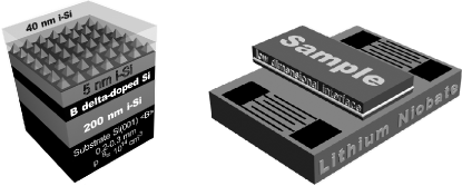
We study B-doped arrays of Ge-in-Si QDs with densities cm-2 and filling factors - 2.85 Stepina2010 . The samples were grown by Stranski-Krastanov molecular beam epitaxy on a (001) Si substrate. The QD array layer was located at 40 nm from the sample surface, see the sketch in the left panel of Fig. 1. QDs are shaped as pyramids with a height of 10-15 Å and a square base having the side of 100-150 Å. The samples were -doped with B, the density in the doped layer being cm-2. In these systems two lowest states in Ge QDs are occupied by holes, and the third level is partly occupied. The 4th state is split from the 3rd one by 18-23 meV Yakimov2001 . Therefore, the 4th level is expected to be empty in the temperature domain of interest.
We studied AC conductance of two samples, which were annealed and were close in conductance. The aim of annealing was increasing of the sample conductance; during the annealing the dots spread and the distance between them decreases from initial 15 nm to almost overlapping. The samples studied in Drichko2005 had larger conductance and therefore AC hopping conductance was not observed there.
Procedure
We used the probeless acoustic method to determine the complex ac conductance, , from attenuation, , and velocity, , of a surface acoustic wave (SAW) induced on the surface of a LiNbO3 piezoelectric crystal by interdigital transducers, see right panel of Fig. 1. The sample is pressed to the crystal surface by a spring. A SAW-induced AC electric field penetrates into the sample and interacts with charge carriers (holes). As a result, both and acquire additional contributions, which can be related to complex Drichko2000 . We single out these contributions by measuring the changes induced by external transverse magnetic field, , and similarly . For these particular samples is not measurable thus indicating that . Therefore, further we will discuss only and . Since the hole absorption vanishes in very high magnetic fields we extrapolate experimentally found to and in this way find versus temperature and SAW frequency at frequencies 30-414 MHz in the temperature domain 1.8-13 K.
Linear regime
Shown in the left panel of Fig. 2 are magnetic field dependences of at MHz and T for different temperatures.
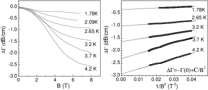
These dependences are replotted in the right panel as functions of , which can be represented as straight lines. The attenuation coefficient at , , is determined by crossing of these lines with the axis . For the situation relevant to present experiment the general expression Drichko2000 relating with can be simplified as
| (1) |
Here is the SAW wave vector, is the piezoelectric coupling constant in the LiNbO3, and are geometric factors given in Drichko2000 , which depend on the dielectric constants of the sample (), vacuum () and substrate (), as well as on the depth of the QD layer and the clearance between the sample and substrate. The above expression is valid provided that is the case in the present situation.
Shown in the left panel of Fig. 3 are temperature dependences of for the sample 1 at frequencies 30.1 and 307 MHz found from Eq. (1). The clearance was determined from Newton’s rings.

Frequency dependence of for the sample 2 at K is shown in the right panel.
Nonlinear regime
Shown in the left panel of Fig. 4 are magnetic field dependences of at frequency MHz at K for different input SAW intensities.
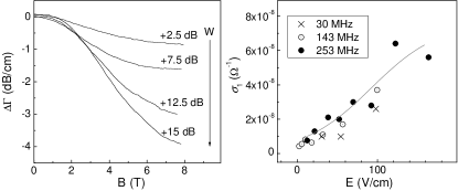
Similarly to the linear regime, the values , and were determined by extrapolation to . The intensities were determined as follows. Firstly, the signal having passed through the system was compared with the input signal from the generator. This comparison allowed determining the transformation losses in both transducers plus the losses in input and output transmission lines (which are considered to be equal). The intensity was changed by synchronous changing of the calibrated attenuators installed after the generator and after the output transducer keeping the summary attenuation (in dB) constant. Knowing the transformation losses in one transducer and in the input line we find the acoustic intensity after the input transducer. Similar measurements were done for , 143 and 253 MHz.
Since for each frequency the inequality (where is the attenuation coefficient in cm-1 while mm is the sample length) is met, one can neglect the difference between the input and output intensities while calculating the typical amplitude of the SAW-induced electrical field. It is evaluated from the energy conservation law . This procedure is valid since due to the inequality higher harmonics of the signal are weak. The obtained in this way dependence for sample 1, at K and different frequencies is shown on the right panel of Fig. 4. One observe very weak frequency dependence.
The regime of weak non-Ohmic behavior ( V/cm) was investigated in more detail for the sample 2 at MHz and different temperatures, , 3.3, 4.2 and 7 K.
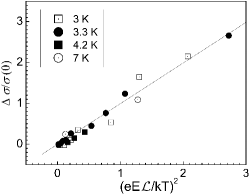
The dependences on dimensionless parameter are shown in Fig. 5. The characteristic length is chosen as cm in order to have at . One observes an approximate data collapse.
III Simulations
Since we are not aware of any analytical theory for AC hopping conduction in dense QD arrays we have performed numerical simulations for a model system consisting of a square lattice of randomly occupied localized states davies . We put having in mind that for this size we know that finite size effects are not appreciable in DC conductance aurora . Each of the states can be either empty or occupied (double occupancy is not allowed). The simulations were performed for the filling factor of 1/2, so that the number of electrons is half the number of sites. Disorder is introduced by assigning a random energy in the range to each site (in our numerics we have used where is the lattice constant). Each site is also given a compensating charge so that the overall system is charge neutral. The charges interact via the Coulomb interaction. In the following the unit of energy is chosen as the Coulomb energy of unit charges on nearest neighbor sites, . The unit of temperature is then .
To simulate the time evolution we used the dynamic Monte Carlo method introduced in Ref. tsigankov for simulating DC transport. The only difference is that we apply an AC electric field and that, following Ref. tenelsen , we use for the transition rate of an electron from site to site the formula
| (2) |
where is the energy of the phonon and is the distance between the sites. contains material dependent and energy dependent factors, which we approximate by their average value; we consider it as constant and its value, of the order of s, is chosen as our unit of time. Consequently, is measured in units of while the electric field is measured in units of . The conductance (in Siemens) is expressed in units of . Note that our model is oversimplified comparing to realistic dense QD arrays. In particular, the model assumes a hydrogen-like wave function with localization length and independent of the phonon wave vector electron-phonon coupling, we ignore dielectric susceptibility of the host, etc. Therefore, we hope to reproduce the behavior of AC conductance only qualitatively. However, we believe that the model reproduces main physics of the dense arrays – interplay between Coulomb correlations and disorder as well as relatively large ratio between and a distance between the dots. To decrease the number of independent parameters we put .
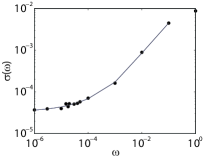
Shown in Fig. 6 (left panel) is the conductance versus frequency for (corresponding to the Efros-Shklovskii regime) and which we know is close to the upper limit of the Ohmic regime for DC transport aurora .
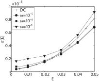
Dependences of on the field amplitude for different frequencies are shown in the right panel. As it is seen, the conductance grows with frequency, as well as with electric field that qualitatively agrees with the experimental results shown in Figs. 3, 4 (right panels).
We can present the results in a different form: assuming that the non-Ohmic behavior is due to heating of the charge carriers we would expect that the conductance at a large field will be the same as the Ohmic conductance at a higher temperature corresponding to the electron temperature. This is known to be approximately true for DC conductivity caravaca ; aurora . Thus, we expect a relation of the form
| (3) |
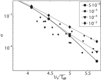
where is the effective electron temperature while is the Ohmic AC conductance. In the simulations we can check the accuracy of this relation by independent calculation of and . The latter was found from direct fitting of the Fermi function to the actual distribution function of occupied sites obtained by averaging over 20 states. We also found the Ohmic conductivity as function of temperature for different frequencies. If relation (3) holds we should find at a given frequency the following: as the electric field is increased, both the effective temperature and the conductivity increase in such a way that the points follow the same curve as the Ohmic conductivity. We plot versus for different frequencies in Fig. 7 (left panel). As we can see, relation (3) is approximately satisfied.
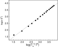
Therefore, we have used it as a definition of the electron temperature allowing us to extract it from experimental data on and . Shown in the right panel of Fig. 7 is the relationship between so-defined and the absorbed power, , for the lattice temperature of K. Here we used averaged data for different frequencies since the frequency dependence is rather weak. The results are compatible with the dependence . Interestingly, a similar dependence was reported for amorphous InOx films, which are on the dielectric side of a insulator-to-superconductor transition ovadia . Though such a dependence was predicted for a metallic state schmid , we are not aware of any analytical theory explaining such a dependence in the insulating phase.
Conclusion
Using acoustic methods we have measured real part of nonlinear AC conductance in insulating 2D arrays of Ge-in-Si QDs. The observed features – inequality , increasing of with the field amplitude, its relatively weak frequency dependence, large energy exchange length – essentially contradict to the predictions of the two-site model discussed in Sec. I. The dissipation is rather due to electron transitions in multi-site clusters. This is not surprising because the two-site model requires the close pairs to be isolated that can be met only in dilute systems. The observed non-Ohmic behavior is attributed to heating of the charge carriers by AC electrical field, as in the DC case Gershenson2000 . We have also performed simulations of AC conductance in a dense 2D lattice of localized states taking into account both distribution of their energies and Coulomb correlations. The results qualitatively agree with experiment confirming the above conclusion.
This work was supported by grant of RFBR 11-02-00223, grant of the Presidium of the Russian Academy of Science, the Program ”Spintronika” of Branch of Physical Sciences of RAS.
References
- (1) M. E. Gershenson, et al. Phys. Rev. Lett. 85, 1718 (2000).
- (2) Z. Ovadyahu, Phys. Rev. B 84, 165209 (2011).
- (3) R. M. Hill, Philos. Mag. 24, 1307 (1971); B. I. Shklovskii, Fiz. Tekh. Poluprovodn. 6, 2335 (1972) [Sov. Phys. Semicond. 6, 1964 (1973)]; N. Apsley and H. P. Hughes, Philos. Mag. 31, 1327 (1975); M. Pollak and I. Riess, J. Phys. C 9, 2339 (1976); B. I. Shklovskii, Fiz. Tekh. Poluprovodn. 10, 1440 (1976) [Sov. Phys. Semicond. 10, 855 (1976)]; B. I. Shklovskii, Fiz. Tekh. Poluprovodn. 13, 93 (1979); I. P. Zvyagin, Phys. Status Solidi B 88, 149 (1978).
- (4) B. I. Shklovskii and A. L. Efros, Electron properties of dopes semiconductors (Springer Verlag, Berlin, 1984).
- (5) A. L. Efros, Zh. Eksp. Teor. Fiz. 89, 1834 (1985) [Sov. Phys. JETP 62, 1057 (1985).
- (6) A. L. Efros and B. I. Shklovskii, in Electron-Electron Interactions in Disordered Systems, edited by A. L. Efros and M. Pollak (North-Holland, Amsterdam, 1985), p. 409.
- (7) Y. M. Galperin, V. L. Gurevich and D.A. Parshin, in Hopping Transport in Solids, edited by B. Shklovskii and M. Pollak (Elsevier, NY, 1991).
- (8) Y. M. Galperin, M. Kirkengen, Phys.Rev.B 56, 13615 (1997); ibid. 62, 16624 (2000).
- (9) I. L. Drichko, A. M.Diakonov, I. Yu. Smirnov, Y. M. Galperin and A.I.Toropov, Phys. Rev. B 62, 7470 (2000).
- (10) N. P. Stepina, E. S. Koptev, A. V. Dvurechenskii and A. I. Nikiforov, Phys.Rev. B 80, 23 (2010).
- (11) A. I. Yakimov, Electronic phenomena in Ge-in-Si quantum dot arrays (in Russian), Dr. Sci. thesis, Novosibirsk (2001).
- (12) I. L. Drichko, A. M. Dyakonov, I. Yu. Smirnov, A. V. Suslov, Y. M. Galperin, A. I. Yakimov and A. I. Nikiforov, Zh. Eksp. Teor. Fiz. 128, 1279 (2005) [Sov. Phys. JETP 101, 1122 (2005)].
- (13) J. H. Davies, P. A. Lee, and T. M. Rice, Phys. Rev. Lett. 49, 758 (1982).
- (14) A. Voje, MD thesis, UiO (2009), http://urn.nb.no/URN:NBN:no-26080.
- (15) D. N. Tsigankov and A. L. Efros, Phys. Rev. Lett. 88, 176602 (2002).
- (16) K. Tenelsen and M. Schreiber, Phys. Rev. B 52, 13287 (1995). A. Díaz-Sánchez et. al., Phys. Rev. B 59, 910 (1999).
- (17) M. Caravaca, A. M. Somoza, M. Ortuño Phys. Rev. B 82, 134204 (2010).
- (18) M. Ovadia, B. Sacépé, and D. Shahar, Phys. Rev. Lett. 102, 176802 (2009).
- (19) A. Schmid, Z. Phys. 271, 251 (1974); M. Reizer and A. Sergeyev, JETP 63, 616 (1986).