Giant magnetoelectric effect in pure manganite-manganite heterostructures
Abstract
Obtaining strong magnetoelectric couplings in bulk materials and heterostructures is an ongoing challenge. We demonstrate that manganite heterostructures of the form show strong multiferroicity in magnetic manganites where ferroelectric polarization is realized by charges leaking from to due to repulsion. Here, an effective nearest-neighbor electron-electron (electron-hole) repulsion (attraction) is generated by cooperative electron-phonon interaction. Double exchange, when a particle virtually hops to its unoccupied neighboring site and back, produces magnetic polarons that polarize antiferromagnetic regions. Thus a striking giant magnetoelectric effect ensues when an external electrical field enhances the electron leakage across the interface.
pacs:
75.85.+t, 71.38.-k, 71.45.Lr, 71.38.Ht, 75.47.Lx, 75.10.-bI Introduction
Complex oxides such as manganites display a rich interplay of various orbital, charge, and spin orders when rare-earth dopants are added to the parent oxide. While significant progress has been made in characterizing the bulk doped materials, the heterostructures produced from two parent oxides is an area of active research ahn ; millis0 . In these heterostructures, the accompanying quantum confinement, anisotropy, heterogeneity, and the enhanced gradients (in magnetic moments, electric potential, orbital polarization, etc.) across the interface result in novel phenomena that have no counter part in the bulk samples pbl1 In fact, the challenge is to technologically exploit this new physics and develop new useful devices that can meet future demands such as miniaturization, dissipationless operation/manipulation (such as read/write capability), energy storage, etc mannhart0 ; mannhart01 ; hwang0 ; spaldin0 ; tokura0 ; dagotto0 ; ramesh0 .
There has been a revival in multiferroic research partly due to improved technology, discovery of new compounds (such as , ), need for devices with strong magnetoelectric effect, etc tsymbal1 . Majority of the multiferroics studied are bulk materials where it is not yet clear why the magnetic and electric polarizations coexist poorly khomskii1 . With the advent of improved molecular-beam-epitaxy technology one can now grow oxide heterostructures with atomic-layer precision and explore the possibility of strong multiferroic phenomena as well as large interplay between ferroelectricity and magnetic polarization. Coupling between the charge and spin degrees of freedom is fascinating both from a fundamental viewpoint as well from an applied perspective. Instead of employing currents and magnetic fields, controlling and manipulating magnetism with electric fields holds a lot of promise as the electric fields are easier to use in smaller dimensions and can potentially lower energy consumption in systems. There are numerous mechanisms for magnetoelectric effect; reviews for these can be found in Refs. khomskii2, ; wang, ; spaldin, ; ramesh1, ; sdong, . At the interface of a magnetic oxide and a ferroelectric/dielectric oxide, magnetoelectric effect of electronic origin has been predicted by some researchers. Upon application of an external electric field, not only the magnitude of moments can be changed spaldin1 ; me9 , but in some cases the very nature of magnetic ordering can be changed tsymbal2 .
Among various efforts pertaining to oxide heterostructures, there is considerable interest, both experimentally anand1 ; anand2 ; anand3 ; anand4 ; schiffer1 ; kawasaki1 ; kawasaki2 ; schlom as well as theoretically millis2 ; millis3 ; satpathy ; dagotto3 ; dagotto1 ; perroni , in understanding novel aspects of conductivity, magnetism, and orbital order in pure manganite-manganite heterostructures where T refers to trivalent rare earth elements La, Pr, Nd, etc. and D referes to divalent alkaline elements Sr, Ca, etc. At low temperatures, the bulk is an insulating A-type antiferromagnet (A-AFM); on the other hand, the bulk is an insulating G-type antiferromgnet (G-AFM). Furthermore, the doped alloy is an antiferromagnet for ; whereas for , it is a ferromagnetic insulator (FMI) at smaller values of x (i.e., ) tokura ; cheong ; raveau and is a ferromagnetic metal at higher dopings in , , , and kalpataru .
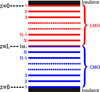
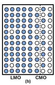
In spite of considerable efforts towards control of magnetization through electric fields in multiferroic bulk materials and heterostructures, obtaining strong magnetoelectric couplings continues to be a challenge. Here, in this paper, we predict a novel giant magnetoelectric effect, not at the interface, but away from it, in a pure manganite-manganite heterostructure (see Fig. 1). Our objective is to present a plausible multiferroic phenomenon in manganite heterostructures and point out the associated unnoticed striking magnetoelectric effect. Cooperative electron-phonon interaction is shown to be key to understanding both multiferroicity and magnetoelectric effect in our oxide heterostructure. Here, we exploit the fact that manganites have various competing phases that are close in energy and that by using an external perturbation (such as an electric or a magnetic field) the system can be induced to alter its phase. We show that there is a charge redistribution (with a net electric dipole moment perpendicular to the interface) and a concomitant ferromagnetism due to the optimization produced by the following two competing effects: (i) energy cost to produce holes on the (LMO) side and excess electrons on the (CMO) side; and (ii) energy gain due to electron-hole attraction (or electron-electron repulsion) on nearest-neighbor sites induced by electron-phonon interaction. The charge polarization is akin to that of a pn-junction in semiconductors although the governing equations are different. The key results of our analysis are as follows: (i) the interface charge density at the LMO-CMO interface is 0.5 electrons/site. The LMO-CMO interface is ferromagnetic and persists to be ferromagnetic for another layer adjacent to the interface on the LMO side; (ii) minority carriers leak across the interface of the heterostructure and produce ferromagnetic domains due to the ferromagnetic coupling (generated by electron-phonon interaction and double-exchange) between an electron-hole pair on adjacent sites; and (iii) since ferroelectricity and ferromagnetism have a common origin [i.e., minority carriers or holes (electrons) on LMO (CMO) side], there is a striking interplay between these two polarizations; consequently, when an external electric field is applied to increase minority carriers, a giant magnetoelectric effect results.
The rest of the paper is organized as follows. In Sec. II we introduce our phenomenological Hamiltonian (based on cooperative electron-phonon-interaction physics) using which we deduce the charge distribution in the continuum approximation. We also provide a simple analytic treatment for the magnetic profile and demonstrate a giant magnetoelectric effect in a few-layered heterostructure. Next, in Sec. III, we adopt a more detailed numerical approach and introduce a Hamiltonian that includes additional kinetic terms, work functions, and discrete lattice effects. Here, magnetoelectric effect is studied in symmetric lattices (involving equal number of LMO and CMO layers) as well as in asymmetric lattices using Monte Carlo simulations. We close in Sec. IV with our concluding observations.
II Analytic treatment
We will begin our treatment of the pure manganite-manganite heterostructure by considering a simple analytic picture in this section. In the next section, we will take recourse to a more detailed numerical approach.
II.1 Polaronic Hamiltonian
In our heterostructure depicted in Fig. 1, due to charge leaking across the LMO-CMO interface, we expect different states of the phase diagram of (LCMO) at different cross-sections perpendicular to the growth direction. Since far from the LMO-CMO interface the material properties must be similar to those in the bulk, we expect the phase at the Insulator-LMO interface and the phase at the other end involving CMO-Insulator interface. Considering majority of the LCMO phase diagram (including the end regions near and ) is taken up by insulating phases, since band width is significantly diminished at strong electron-phonon coupling, and because the heterostructures are quasi two-dimensional (2D), we expect that there is no effective transport in the direction normal to the oxide-oxide interface (i.e., the z-direction). Then, for analyzing the charge distribution normal to the interface, the starting polaronic Hamiltonian is assumed to comprise of localized electrons and have the following phenomenological form:
| (1) |
where the first coefficient is due to electron-phonon interaction and represents nearest-neighbor electron-electron repulsion brought about by incompatible distortions of nearest-neighbor oxygen cages surrounding occupied ions. The pre-factor can depend on the phase – for instance, in the regime of C-type antiferromagnet (C-AFM) in LCMO, is expected to be large because occupancy of neighboring orbitals is inhibited in the z-direction; while in the regime of A-AFM (corresponding to undoped ), is expected to be weaker because of compatible Jahn-Teller distortions on neighboring sites. Here, we will assume for simplicity that is concentration independent and that . Next, the coefficient results from processes involving hopping to nearest-neighbor and back and is present even when we consider the simpler Holstein model sdadsy1 or the Hubbard-Holstein model srsypbl1 . The pre-factor varies between (for non-cooperative electron-phonon interaction) and (since for cooperative breathing mode in one-dimensional chains , which should be more than in C-chains) rpsy . Now, even within the two-band picture of manganites in Ref. tvr, , the electrons in the localized polaronic band contribute the term ; the broad band (due to undistorted states that are orthogonal to the polaronic states) is an upper band whose band width is reduced due to the 2D nature of the system and does not overlap with the polaronic band to produce conduction even at carrier concentrations corresponding to . Furthermore, although is the total number in both the orbitals at site , it can only take a maximum value of 1 due to strong on-site electron-electron repulsion and strong Hund’s coupling. Next, to make the above Hamiltonian furthermore relevant for manganites, one needs to consider Hund’s coupling between core spins and itinerant electrons. This leads to invoking the double exchange mechanism for transport. Then, the hopping term between sites and in Eq. (1) is modified to be with being the core spin at site and being the angle between and . The term in Eq. (1) produces a strong ferromagnetic coupling between the spins at site and site and this dominates over any superexchange coupling between the two spins.
II.2 Charge Profile
To obtain the charge distribution, we ignore the effect of superexchange interaction in the starting effective Hamiltonian in Eq. (1) because its energy scale is significantly smaller that the polaronic energy term . For a localized system, we only need to minimize the interaction energy which is a functional of the electronic density profile. The Coulombic interaction energy resulting from the electrons leaking from the LMO side to the CMO side, is taken into account by ascribing an effective charge (hole) to the LMO unit cell (centered at the site) that has donated an electron from the site and an effective charge (electron) to the CMO unit cell (centered at the site) that has accepted an electron at the site. The Coulombic energy that results is due to the interactions between these effective charges. The net positive charge on the LMO side and the net negative charge on the CMO side will produce a charge polarization (or inversion asymmetry). Since the ferroelectric dipole is expected to be in the direction perpendicular to the oxide-oxide (LMO-CMO) interface, we assume that the density is uniform in each layer for calculating the density profile as a function of distance from the insulator-oxide interface. The Coulombic interaction energy per unit area due to leaked charges is the same for both LMO and CMO regions and is given, in the continuum approximation, to be
| (2) |
where is the electric displacement and is given by
| (3) |
with () sign for LMO (CMO) side. Furthermore, is the denisity of minority charges (i.e., holes on LMO side and electrons on SMO side), the charge of a hole, the dielectric constant, an external electric field along the z-direction, and the thickness of the LMO (CMO) layers.
The ground state energy per unit area [corresponding to the effective Hamiltonian of Eq. (1)] can be written, in the continuum approximation, as a functional of for both LMO and CMO as follows:
| (4) |
where is the coordination number and is the lattice constant. In arriving at the above equation we have approximated . Furthermore, for the ground state, we expect , i.e., the minority charges will completely polarize the neighboring majority charges.
We will now minimize the total energy given below
| (5) |
by setting the functional derivative =0. This leads to the following equation
where ; ; and . The above equation, upon taking double derivative with respect to , yields
| (7) |
The above second-order differential Eq. (7) and Eq. (LABEL:E_opt) admit the solution
| (8) |
where .
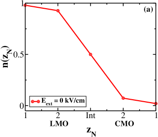
It is important to note that, for
the manganese-oxide (MO) layer
at the LMO-CMO interface (i.e., at ), the density is 0.5 electrons/site
and that it is
independent of the applied external electric field
and the system parameters. Now, since each site
in the interface layer belongs to a unit cell that is half LMO and half CMO, one expects the
density per site to be 0.5. Additionally, we observe from Eq. (8) that for smaller
values of , as distance from the LMO-CMO interface increases, the density falls more rapidly while
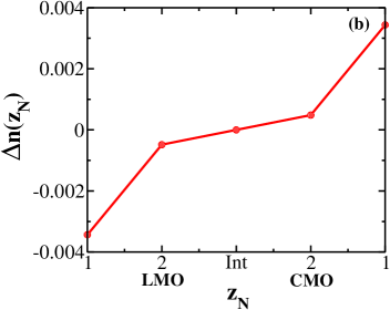
the density change due to electric field rises faster. Furthermore,
for realistic values of the parameters, the charge density
rapidly changes as we move away
from the oxide-oxide interface (i.e., after only a few layers from the interface) and
attains values close
to the bulk value [as illustrated in Fig. 2(a)]. Lastly, as required for zero values
of the external field , we get when .
Thus, although we used the continuum approximation, our obtained density
profile is qualitatively realistic as it has the desired values at the extremes
and with the density away from the LMO-CMO interface rapidly falling for not too large values of
.
The density profiles for both LMO and CMO sides depend only on , and . For our calculations displayed in Figs. 2(a) and 2(b), we used the following values for the parameters: Å; ; ; and [based on ; ; and ].
II.3 Magnetization distribution
We will now obtain the magnetization for a heterostructure by considering its lattice structure unlike the case for the density profile where a continuum approximation was made. Thus we can take into account the possibility of antiferromagnetic (AFM) order besides being able to consider ferromagnetic (FM) order.
First, we observe that the bulk (below the magnetic transition temperatures) is A-AFM for and a ferromagnet for . Hence, we model the LMO side of the heterostructure as an A-AFM when hole concentrations are small; whereas at higher concentrations of holes which is less than 0.5, the holes dictate the magnetic order by forming magnetic polarons that polarize the A-AFM. Next, we note that for , the bulk system is always an antiferromagnet. Thus, from a magnetism point-of-view, the magnetic moment on the CMO side of the heterostructure is expected to be zero except in the vicinity of the interface where (due to proximity effect) it will be a ferromagnet and can be modeled using a percolation picture. Given the above scenario, as can be expected, we find that the ferromagnetic region on the LMO side can be drastically enhanced (at the expense of the A-AFM region) by an electric field inducing holes on the LMO side. On the other hand, the electric field has only a small effect on the percolating ferromagnetic cluster that is adjacent to the oxide-oxide interface on the CMO side.
II.3.1 CMO side
We will first consider the CMO side and show that the magnetization decays as we move away from the LMO-CMO interface. We derive below the largest FM domain; this domain percolates from the LMO-CMO interface. On account of nearest-neighbor repulsion (as given in Eq. (1)), the interface (which is half-filled) has electrons on alternate sites. In fact, to minimize the interaction energy, on the CMO side we take the electrons to be in one sublattice only which will be called -sublattice; the other unoccupied sublattice will be called the -sublattice. On account of virtual hopping, an electron polarizes all its neighboring sites that do not contain any electrons and forms a magnetic polaron. Thus we observe that the half-filled interface will be fully polarized and that there will be a FM cluster that begins at the interface and percolates to the layers away from the interface on the CMO side. For instance, in the layer next to the oxide-oxide interface, all the electrons are in the same sublattice (the -sublattice) and are next to the empty sublattice (i.e., sublattice unoccupied by electrons) of the interface and hence are ferromagnetically aligned with the interface. Similarly, again in the layer adjacent to LMO-CMO interface, all the sites in the other sublattice (i.e., the -sublattice) are empty and have the same polarization as the sites occupied by the electrons at the interface.
We will now identify the equations governing the ferromagnetic cluster percolating from the interface. Let be the -coordinate of the 2D MO layer with being the index measured from the Insulator-CMO interface (as shown in Fig. 1). Furthermore, we define () as the concentration of polarized sites that belong to the spanning cluster and these sites are a subset of the sites in the -sublattice (-sublattice) in the 2D MO layer. Then, the factor [] represents the probability of a site that belongs to the -sublattice (-sublattice) in layer N but is not part of the spanning polarized cluster. Now, the probability that a site, occupied (unoccupied) by an electron, contributes to the FM cluster is equal to the probability of finding the site occupied (unoccupied) multiplied by 1-P where P is the probability that none of the adjacent sites that are in the -sublattice (-sublattice) belong to the percolating cluster. Therefore, we obtain the following set of coupled equations for the spanning cluster:
| (9) |
| (10) |
The boundary conditions involving layer 1 are
| (11) |
and
| (12) |
while those for the LMO-CMO interface are .
II.3.2 LMO side
Next, we will show that the LMO side with only a few layers, for some realistic values of parameters, can have a sizeable change in the magnetism when a large electric field is applied and thus can be exploited to obtain a giant magneto-electric effect. Similar to the bulk situation in khali ; super_ex , in our heterostructure as well, we assume that two spins on any adjacent sites in each MO layer have a ferromagnetic coupling ; whereas, any two neighboring spins on adjacent layers have an antiferromagnetic coupling . On the other hand, for an electron and a hole on neighboring sites either in the same MO layer or in adjacent MO layers, (due to virtual hopping of electron between the two sites) there is a strong ferromagnetic coupling tvr . In our calculations, as long as the ratio of is taken as fixed and is the significantly dominant coupling, we get the same magnetic picture.
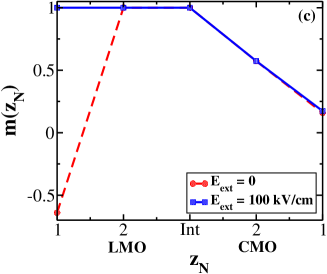
In a LMO side with a few MO layers, to demonstrate the possibility of large magnetization change upon the application of a large external field, we assume that the LMO-CMO interface and all MO layers up to layer M are completely polarized. Next, we assume that MO layers M and M-1 have low density of holes so that there is a possibility that spins in MO layer M-1 are not aligned with the block of MO layers starting from the LMO-CMO interface and up to layer M. We then analyze the polarization of MO layer M-1 by comparing the energies for the following two cases: (i) layers M-1 and M are antiferromagnetically aligned with the holes in layers M and M-1 inducing polarization only on sites that are adjacent to the holes; and (ii) MO layer M-1 is completely polarized and aligned with Layer M.
In a few-layered heterostructure , for eV (as shown in Fig. 2(c), we obtain a striking magneto-electric effect. For zero external field, when is considered, case (i) (mentioned above) has lower energy, i.e., layer 1 is antiferromagnetically coupled to layer 2. On the other hand, when a strong electric field () is applied, MO layer 1 (due to increased density of holes) becomes completely polarized and ferromagnetically aligned with the rest of the layers (i.e., MO layer 2 and the oxide-oxide interface) on the LMO side. Thus, we get a giant magneto-electric effect!
III Numerical Approach
Here, in this section, we construct a detailed 2D model Hamiltonian and study it numerically for the charge and magnetic profiles and the coupling between them.
III.1 Model Hamiltonian
In a quasi 2D heterostructure (involving only a few 2D layers of both manganites), as mentioned in Sec. II, we expect only a single narrow-width polaronic band to be relevant tvr . For our numerical treatment of a 2D lattice (with rows and columns), we employ the following one-band Hamiltonian:
| (13) |
The kinetic energy term is given by
| (14) |
where is the hopping amplitude that is attenuated by the electron-phonon coupling , is the electron destruction operator, and is the modulation due to infinite Hund’s coupling between the itenerant electrons and the localized spins with being the angle between two localized spins at sites and . The second term in Eq. (13) is the mean-field version of in Eq. (1) and is expressed as
| (15) | |||||
where refers to the mean number density at site . A derivation of is given in Ref. rpsy, ; however, for simplicity, here we have ignored the effect of next-nearest-neighbor hopping. The next term in Eq. 13) pertains to the superexchange term which generates A-AFM in and G-AFM in ; thus on the side, it is given by
| (16) |
while on the side, we express it as
| (17) |
In the above superexchange expressions, the magnitude of the spins is absorbed in the superexchange coefficients and . It should be clear that, away from the LMO-CMO interface, we can recover the spin arrangements of bulk and ; whereas, near the interface the minority carriers are expected to modify the spin textures. In Eq. (13), the Coulomb interaction is accounted for through the term as follows:
| (18) |
where the first term on the right hand side (RHS) is actually the on-site Coulomb interaction between an electron and a positive ion that yields the binding energy of an electron and is therefore applicable only to the LMO side. The remaining term on the RHS of Eq. (18, denotes long-range, mean-field Coulomb interactions between electrons as well as between electrons and positive ions. Here, represents the positive charge density operator with a value of either 1 or 0 and is the distance between lattice sites and . Furthermore, the dimensionless parameter determines the strength of the Coulomb interaction. Lastly, in Eq. (13), the term represents the potential felt at various sites due to an externally applied potential difference () between the two insulator edges (see Fig. 1):
| (19) |
where I represents the layer (or column) index with denoting the number of layers, i.e., the number of sites in the z-direction; K represents the row index with denoting the number of rows, i.e., the number of sites in a layer.
III.2 Calculation procedure
We consider a 2D lattice involving a few layers (columns) of LMO and CMO and study magnetoelectric effect. The lattice does not have periodicity in the direction normal to the interface of the heterostructure (i.e., the z-direction). On the other hand, to mimic infinite extent in the direction parallel to the interface of the heterostructure, we assume periodic boundary condition in that direction. We employ classical Monte Carlo with Metropolis update algorithm to obtain the charge and magnetic profiles for our 2D lattice. To tackle the difficult problem of several local minima that are close in energy, we take recourse to the simulated annealing technique. To arrive at a reasonable charge profile at energy scales much larger than the superexchange energy scale, we treat the problem classically (i.e., fully electrostatically) by considering only the Coulomb term (), the external-potential term (), and the electron-phonon-interaction term [] as these are the dominant energy terms in the Hamiltonian. The Coulomb term is subjected to mean field analysis (as mentioned before) and the system generated potential millis in Eq. (18) is solved self-consistently. This is equivalent to solving the Poisson equationdagotto2 .
Next, to arrive at the final charge and magnetic configurations, we treat the system quantum mechanically by starting with an initial configuration comprising of the charge configuration generated classically (by the above procedure) and an initial random spin configuration. We now consider the full Hamiltonian, where hopping term () and spin interaction energy act as perturbation to the classical dominant energy terms [, , and ], thereby allowing for a small change in the number density profile and determine the concomitant magnetic profile. For the classical spins that are normalized to unity, the and values are binned in the intervals and respectively with equally spaced 40 values of and 80 values of , hence yielding a total of 3200 different possibilities.
In our calculations, we employ the parameter values , , and leading to a small parameter value . For our manganite heterostructure, lattice constant Å, dielectric constant , magnetic couplings and ; we take the pre-factors [in Eq. (15)] and . The coefficient in Eq. (18), representing the relative work function of the LMO side with respect to the CMO side, is taken to be ; hence the confining radius for the electron is 1.33 Åwhich is less than half the lattice constant. External potential diferences , corresponding to external electric fields and (which are less than the breakdown field in LCMO ramesh ), are applied to study changes in the magnetization profiles.
The simulation (involving the charge and spin degrees of freedom) is carried out using exact diagonalization of the total Hamiltonian in Eq. (13). The spins are annealed over 61 values of the dimensionless temperature [], in steps of 0.05, starting from 3 and ending at 0.05 with 15000 system sweeps carried out at each temperature. Since hopping energy , the inclusion of the spin degrees of freedom certainly commenses at temperatures . Furthermore, the endpoint is sufficiently small to correspond to the ground state of the system. Each sweep requires visiting all the lattice sites sequentially and updating the spin configuration at each lattice site by the standard Metropolis Monte Carlo algorithm. We are also allowing the charge degrees of freedom to relax by treating the problem self-consistently. So, at the beginning of each sweep, the Poisson equation is solved additionally to make sure that the number densities have converged and this is achieved with an accuracy of 0.001. Finally, averages of the various measurables in the system are taken over the last 5000 sweeps in the system.
III.3 Results and discussion
For numerical simulation, we consider two lattice sizes, namely, and with number of rows and number of layers (columns) or . Here, all the sites in each layer belong solely to either LMO or CMO. This is in contrast to the continuum approximation employed in Sec. II.2 to obtain the charge profile analytically. In Sec. II.2, by exploiting the symmetry of the interactions of the minority carriers on both sides of the LMO-CMO interface, we derived the charge profile with charge density always at the interface; this corresponds to a system comprising of odd number of layers with the interface layer being shared equally by the LMO and CMO sides, i.e., each site (in the interface layer) belongs to a unit cell that is half LMO and half CMO.
We consider various situations in our lattices. First, we analyze the case of excluding electron-phonon interaction; consequently, the Hamiltonian of interest is that given by Eq. (13), but without the term. Next, we study the charge and magnetic profiles predicted by the total Hamiltonian of Eq. (13) for the symmetric situation (of equal number of LMO and CMO layers) and for different sizeable values of the electron-phonon coupling, i.e., for . Lastly, we examine the impact on the magnetoelectric effect due to the asymmetry in number of LMO and CMO layers.
III.3.1 No electron-phonon interaction and
Here, without the electron-phonon interaction, the hopping amplitude is not attenuated
by the factor and the ground state is a superposition of various states
in the occupation number representation. The electrons are not localized and we do not
need to employ simulated annealing; the calculations were performed at
a single temperature on a symmetric heterostructure defined
on a lattice with equal number of layers on the LMO side and the CMO side.
Furthermore,
the charge density profile is essentially dictated by the
Coulombic term in Eq. (13); the kinetic term and the superexchange term
have a negligible effect. Thus,
we have density close to 1 on the LMO side and an almost zero density on the CMO side.
Now, when a large electric
field (400 ) is applied, a small amount of charge
gets pushed across the interface. Then, since the kinetic term is much larger
than the superexchange term, double exchange
tries to ferromagnetically align the spins
and, as shown in
Figs. 3 and 4,
we get a large change in the total magnetization
of spins
of the system, i.e.,
0.64/site for the case
and 0.91/site for the case
when spins are normalized to unity.
In manganites the electron-phonon interaction is quite strong and leads to sizeable cooperative oxygen octahedra distortions. Hence, to get a more realistic picture, we switch on this interaction and study its effect on the system. Then, the hopping amplitude is attenuated by the factor and the electrons are essentially localized. Consequently, the states are more or less classical in nature with number density at each site close to 1 (i.e., from our calculations) or close to 0 (i.e., from our numerics); the state of the system can be represented by a single state in the occupation number representation. As discussed in Sec. III.2, we employ simulated annealing; we arrive at the charge and magnetic profiles reported in the subsequent Secs. III.3.2–14.
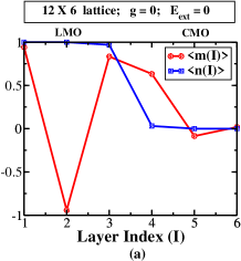
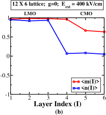
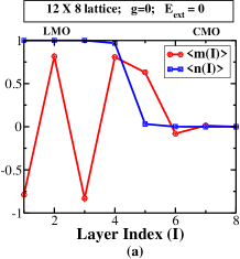
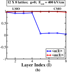
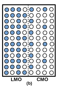
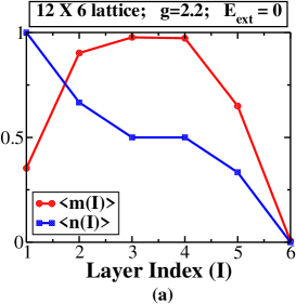
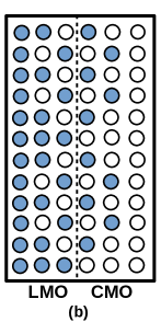
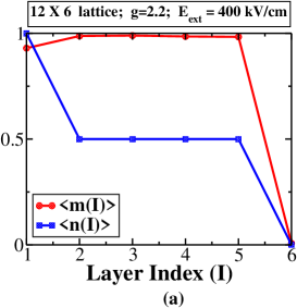
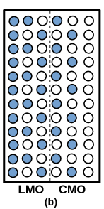
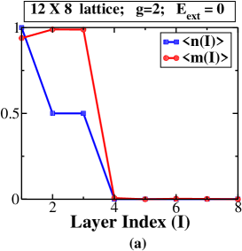
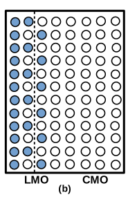
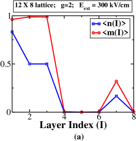
III.3.2 Symmetric lattice with and
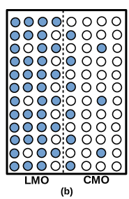
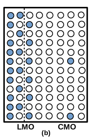
We now consider a symmetric lattice with 4 layers of LMO and another 4 layers of CMO as shown in Figs. 5 and 6. We find charge modulation in the z-direction on both the sides, with neutral layers (free of minority carriers) sandwiched between charged layers (with minority carriers). The layers at the interface have the largest number of minority carriers with electrons and holes on alternate sites as contributions from both and [given by Eqs. (1) and (18)] are minimized for this arrangement. Layers 1 and 8, being the farthest from the LMO-CMO interface, are devoid of any minority carriers and retain the expected bulk charge distribution of LMO and CMO.

We will now explain the charge modulation as follows. We compute the energy electrostatically for the one-dimensional chain in Fig. 7 using in Eq.(18), with lattice constant taken as unity and the number of the neutral layers/sites as . Then
| (20) |
If we plot as a function of , we find that it drops rapidly till and attains its minimum value gradually somewhere between and . Similarly, we expect neutral layers to be present in 2D also and conclude that the charge ordering sets in due to electrostatic Coulomb energy minimization.
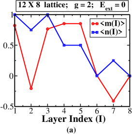
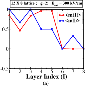
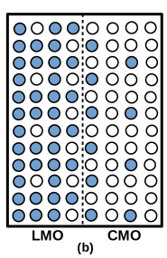
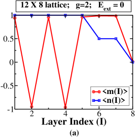
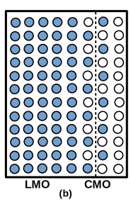
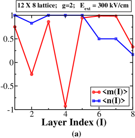
In Figs. 5 and 6, the interface is fairly polarized since the arrangement of electrons and holes on alternate sites produces a strong ferromagnetic coupling between the spins on these sites as . Furthermore, again due to ferromagnetic couplings and on the LMO side, the interfacial layer polarizes the neutral layer 3 adjacent to it. Layer 1 is polarized in the direction of layer 3 due to antiferromagnetic coupling . On the CMO side, layer 6 is antiferromagnetic based on the charge configuration; layer 8, as expected, is also fully antiferromagnetic. As regards the case of zero electric field shown in Fig. 5, since layer 3 is antiferromagnetically connected to layer 2, layer 2 shows a small negative magnetization with the magnitude diminished due to the presence of a few (i.e., 3) holes in this layer. On the application of a large electric field , number of minority carriers increases in both layer 2 and layer 7. Consequently, the magnetization increases in these layers. On the application of the external electric field, there is an overall increase in the magnetization (of normalized-to-unity spins) by 0.17/site leading to a giant magnetoelectric effect.
III.3.3 Symmetric lattice with and

Here we would like to point out that charge and magnetic profiles, when electron-phonon coupling is strong and external electric field is zero, are similar to the profiles when coupling is weak and external electric field is strong. In fact, as can be seen from Figs. 8 and 6, for and we get the same charge profile as when and ; the corresponding magnetic profiles in the two cases differ slightly because the ferromagnetic coupling values are slightly different.
III.3.4 Symmetric lattice with and
Since the electron-phonon interaction is stronger (i.e., ) compared to the situation in Sec. III.3.2, even without the application of an external electric field, the concentration of minority carriers is higher (on both LMO side and CMO side) as can be seen from Figs. 9 and 5. Again, as depicted in Fig. 9, the interfacial layers (i.e., layers 3 and 4) have electrons and holes on alternate sites resulting in full ferromagnetism. Here, we have fewer layers compared to the case in Sec. III.3.2; there is no charge modulation in the z-direction because shifting the holes from layer 2 to layer 1 increases the number of nearest-neighbor repulsions due to electron-phonon interactions. Layers 2 and 5 also have a sizeable density of minority carriers (i.e., 1/3). Consequently, layer 2 is polarized due to its proximity to layer 3 and the ferromagnetic couplings and ; contrastingly, the combination of and the antiferromagnetic coupling lead to a smaller polarization in layer 5. Layer 1, due to its proximity to layer 2 (with sizeable concentration of holes) is also partially polarized. On the application of a large electric field (), as portrayed if Fig. 10, the concentration of holes further increases in layers 2 and 5 leading to fully ferromagnetically aligning these layers with layers 3 and 4. Furthermore, layer 1 also gets more polarized. On the whole, total magnetization (of normalized-to-unity spins) increases by /site thus producing a giant magnetoelectric effect.
III.3.5 Asymmetric system of 2 LMO layers and 6 CMO layers with and
We have an asymmetry here regarding the number of layers; the LMO side has two layers whereas the CMO side has six layers. For zero external electric field, as shown in Fig. 11, the two interfacial layers 2 and 3 contain perfectly alternate arrangement of electrons and holes; hence, the layers are fully polarized. Layer 1 is also ferromagnetically aligned with layer 2 because of their proximity. Beyond layer 3, similar to the G-AFM order in bulk CMO, the CMO side is antiferromagnetic, resulting in zero magnetization. Turning on the sizeable electric field , as depicted in Fig. 12, leads to a few electrons from layer 1 ending up in a farther layer 7; resultantly, the magnetic polarons in layer 7 partially polarize it. It is interesting to note that, here too charge modulation occurs due to the Coulomb term as demonstrated through Eq. (20). There is an overall increase in the magnetization (of normalized-to-unity spins) by 0.04/site; thus, the magnetoelectric effect is not huge.
III.3.6 Asymmetric system of 6 LMO layers and 2 CMO layers with and
Here, compared to the previous stucture in Figs. 11 and 12, we have the opposite asymmetric structure of 6 LMO layers and 2 CMO layers (see Figs. 13 and 14). Due to the asymmetry connection between these two structures, we obtain a mirror image of the previous charge configuration for both with and without the external electric field. The interfacial layers 6 and 7, as expected, are totally ferromagnetic. Furthermore, layer 5 is also ferromagnetically aligned with layers 6 and 7 due to the ferromagnetic couplings and . At zero external field (as shown in Fig. 13), similar to the bulk situation, we have A-AFM on the LMO side up to layer 5; layer 8, similar to the bulk CMO, is also antiferromagnetic. The minority carriers, generated due to the external electric field (as shown in Fig. 14), produce magnetic polarons which increase the polarization. There is an overall increase in the magnetization (of normalized-to-unity spins) by about 0.1/site implying a large magnetoelectric effect.
From the various symmetric and asymmetric LMO-CMO configurations considered, we conclude that the symmetric arrangement yields the largest magnetoelectric effect.
IV CONCLUSIONS
We used the heuristic notion that, when the two Mott insulators LMO and CMO are brought together to form a heterostructure, one may realize the entire phase diagram of across the heterostructure with the phase occurring at the LMO surface at one end and evolving to the state at the oxide-oxide interface and finally to the phase at the other end of CMO. However, owing to the reduced dimensions (namely, quasi two-dimensions), we expect only A-AFM and FMI phases on the LMO side. On enhancing the minority carrier density (on both sides of the interface) by using a sizeable external electric field, we showed that the FMI region can be further expanded at the expense of the A-type AFM region on the LMO side and the G-AFM domain on the CMO side, thereby producing a giant magnetoelectric effect.
As a guide to designing magnetoelectric devices, we find that symmetric heterostructures with equal number of LMO and CMO layers yield larger magnetoelectric effect compared to asymmetric heterostructures with unequal number of LMO and CMO layers.
We also would like to mention that if a superlattice were formed from the heterostructure , then the dipoles from each repeating heterostructure unit will add up to produce a giant electric dipole moment; furthermore, this superlattice will also realize a giant magnetoelectric effect. On the other hand, if the insulator layers were not present, the superlattice formed from the repeating unit would not produce a large electric dipole as the charge from LMO can leak to CMO on both sides leading to a small net dipole moment. More importantly, the superlattice will also not generate a giant magnetoelectric effect as an applied electric field will not alter much the total amount of charge in LMO or CMO; this is because charge leaked by LMO to CMO on one side is replaced by CMO on the other side.
Based on the above arguments, it should be clear that, compared to experiments involving superlattices where alloy/bulk effect vanishes when the thinner side of the repeating unit has more than two layers, in our heterostructure bulk nature should vanish when the thinner side has more than 1 layer. Thus, in the superlattice studied in Ref. anand1, , the metallic behavior (corresponding to bulk ) diappears for and is replaced by insulating behavior; whereas, in the heterostructure we expect insulating behavior for . This observation supports our assumption that, in our quasi 2D LMO-CMO heterostructures (corresponding to LCMO that has a narrower band width compared to LSMO), only a single narrow-width polaronic band is pertinent.
Lastly, it should also be pointed out that, in a realistic situation, we have electron-electron repulsion (produced by cooperative electron-phonon interaction) and double-exchange generated ferromagnetic coupling extending to next-nearest-neighbor sites ravindra2 leading to a larger magnetic polaron and thus producing a stronger magnetoelectric effect compared to what our calculations reveal.
V acknowledgements
S. P. acknowledges useful discussions with S. Nag, R. Ghosh, S. Kadge, N. Swain, S. Mukherjee, and R. Raman. Work at Argonne National Laboratory is supported by the U.S. Department of Energy, Basic Energy Sciences Materials Science and Engineering, under contract no. DE-AC02-06CH11357.
References
- (1) C. H. Ahn, A. Bhattacharya, M. Di Ventra, J. N. Eckstein, C. Daniel Frisbie, M. E. Gershenson, A. M. Goldman, I. H. Inoue, J. Mannhart, Andrew J. Millis, Alberto F. Morpurgo, Douglas Natelson, and Jean-Marc Triscone, Rev. Mod. Phys. 78, 1185 (2006).
- (2) J. Chakhalian, J. W. Freeland, A. J. Millis, C. Panagopoulos, and J. M. Rondinelli, Rev. Mod. Phys. 86, 1189 (2014).
- (3) One striking example is the interface of system reported in A. Ohtomo and H. Hwang, Nature 427, 423 (2004); N. Reyren, S. Thiel, A. D. Caviglia, L. Fitting-Kourkoutis, G. Hammerl, C. Richter, C. W. Schneider, T. Kopp, A. S. Ruetschi, D. Jaccard, M. Gabay, D. A. Muller, J. M. Triscone, and J. Mannhart, Science 317, 1196 (2007); A. Brinkman, M. Huijben, M. van Zalk, J. Huijben, U. Zeitler, J. C. Maan, W. G. van der Wiel, G. Rijnders, D. H. A. Blank, and H. Hilgenkamp, Nat. Mater. 6, 493 (2007); D. A. Dikin, M. Mehta, C. W. Bark, C. M. Folkman, C. B. Eom, and V. Chandrasekhar, Phys. Rev. Lett. 107, 056802 (2011); N. C. Bristowe, Emilio Artacho, P. B. Littlewood, Phys. Rev. B 80, 045425 (2009); N. C. Bristowe, P. B. Littlewood, Emilio Artacho, J. Phys.: Condens. Matter 23, 081001 (2011).
- (4) J. Mannhart and D. G. Schlom, Science 327, 1607 (2010).
- (5) H. Boschker and J. Mannhart, arXiv:1607.07239v1.
- (6) H. Takagi and H. Y. Hwang, Science 327, 1601 (2010).
- (7) G. Hammerl and N. Spaldin, Science 332, 922 (2011).
- (8) H. Y. Hwang, Y. Iwasa, M. Kawasaki, B. Keimer, N. Nagaosa, and Y. Tokura, Nat. Mater. 11, 103 (2012).
- (9) E. Dagotto, Science 318, 1076 (2007).
- (10) L. W. Martin and R. Ramesh, Acta Materialia 60, 2449 (2012)
- (11) For a review see J. P. Velev, S. S. Jaswal and E. Y. Tsymbal, Phil. Trans. R. Soc. A 369, 3069 (2011).
- (12) D.I. Khomskii, J. Magn. Magn. Mater, 306, 1 (2006).
- (13) D. Khomskii, Phys. 2, 20 (2009͒).
- (14) K. F. Wang, J. M. Liu, and Z. F. Ren, Adv. Phys. 58, 321 (2009͒).
- (15) M. Fiebig and N. A. Spaldin, Eur. Phys. J. B 71, 293 (2009).
- (16) P. Yu, Y.-H. Chu, and R. Ramesh, Mater. Today 15, 320 (2012).
- (17) X. Huang and S. Dong, Mod. Phys. Lett. B 28, 1430010 (2014).
- (18) J. M. Rondinelli, M. Stengel,and N. A. Spaldin, Nat. Nanotechnol. 3, 46 (2008).
- (19) M. K. Niranjan, J. D. Burton, J. P. Velev, S. S. Jaswal, and E. Y. Tsymbal, Appl. Phys. Lett. 95, 052501 (2009͒).
- (20) J. D. Burton and E. Y. Tsymbal, Phys. Rev. B 80, 174406 (2009).
- (21) A. Bhattacharya, S. J. May, S. G. E. te Velthuis, M. Warusawithana, X. Zhai, Bin Jiang, J.-M. Zuo, M. R. Fitzsimmons, S. D. Bader, and J. N. Eckstein, Phys. Rev. Lett. 100, 257203 (2008).
- (22) S. Smadici, P. Abbamonte, A. Bhattacharya, X. Zhai, B. Jiang, A. Rusydi, J. N. Eckstein, S. D. Bader, and Jian-Min Zuo, Phys. Rev. Lett. 99, 196404 (2007).
- (23) S. J. May, A. B. Shah, S. G. E. te Velthuis, M. R. Fitzsimmons, J. M. Zuo, X. Zhai, J. N. Eckstein, S. D. Bader, and A. Bhattacharya, Phys. Rev. B 77, 174409 (2008͒).
- (24) A. Bhattacharya, X. Zhai, M. Warusawithana, J. N. Eckstein, and S. D. Bader, Appl. Phys. Lett. 90, 222503 (2007͒).
- (25) C. Adamo, X. Ke, P. Schiffer, A. Soukiassian, M. Warusawithana, L. Maritato, and D. G. Schlom Appl. Phys. Lett. 92, 112508 (2008).
- (26) T. Koida, M. Lippmaa, T. Fukumura, K. Itaka, Y. Matsumoto, M. Kawasaki, and H. Koinuma, Phys. Rev. B 66, 144418 (2002͒).
- (27) H. Yamada, M. Kawasaki, T. Lottermoser, T. Arima, and Y. Tokura, Appl. Phys. Lett. 89, 052506 (2006͒).
- (28) E. J. Monkman, C. Adamo, J. A. Mundy, D. E. Shai, J. W. Harter, D. Shen, B. Burganov, D. A. Muller, D. G. Schlom, and K. M. Shen, Nat. Mater. 11, 855 (2012).
- (29) C. Lin, S. Okamoto, and A. J. Millis, Phys. Rev. B 73, 041104(R͒) (2006).
- (30) C. Lin and A. J. Millis, Phys. Rev. B 78, 184405 (2008).
- (31) B. R. K. Nanda and S. Satpathy, Phys. Rev. B 78, 054427 (͑2008).
- (32) S. Dong, R. Yu, S. Yunoki, G. Alvarez, J.-M. Liu, and E. Dagotto, Phys. Rev. B 78, 201102(R͒) (2008).
- (33) R. Yu, S. Yunoki, S. Dong, E. Dagotto , Phys. Rev. B 80 125115 (2009).
- (34) C. Adamo, C. A. Perroni, V. Cataudella, G. De Filippis, P. Orgiani, and L. Maritato, Phys. Rev. B 79, 045125 (2009).
- (35) Y. Tokura, Rep. Prog. Phys. 69, 797 (2006).
- (36) see K.H. Kim, M. Uehara, V. Kiryukhin and S.-W. Cheong, in Colossal Magnetoresistive Manganites, edited by T. Chatterji, (Kluwer Academic, Dordrecht, 2004).
- (37) C. Martin, A. Maignan, M. Hervieu, and B. Raveau, Phys. Rev. B 60, 12191 (1999).
- (38) For representative studies of doped manganite-manganite heterostructures, see K. Pradhan and A. P. Kampf, Phys. Rev. B 88, 115136 (2013); J. Salafranca, M. J. Calderón, and L. Brey, Phys. Rev. B 77, 014441 (2008͒).
- (39) S. Datta, A. Das, and S. Yarlagadda, Phys. Rev. B 71, 235118 (2005).
- (40) S. Reja, S. Yarlagadda, and P. B. Littlewood, Phys. Rev. B 84, 085127 (2011).
- (41) R. Pankaj and S. Yarlagadda, Phys. Rev. B 86, 035453 (2012).
- (42) G. V. Pai, S. R. Hassan, H. R. Krishnamurthy, and T. V. Ramakrishnan, Europhys. Lett. 64, 696 (2003); T. V. Ramakrishnan, H. R. Krishnamurthy, S. R. Hassan, and G. V. Pai, Phys. Rev. Lett. 92, 157203 (2004).
- (43) A. Szewczyk, M. Gutowska and B. Dabrowski, Phys. Rev. B 72, 224429 (2005).
- (44) N. N. Kovaleva, Andrzej M. Oleś, A. M. Balbashov, A. Maljuk, D. N. Argyriou, G. Khaliullin, and B. Keimer, Phys. Rev. B 81, 235130 (2010).
- (45) K. Hirota, N. Kaneko, A. Nishizawa, and Y. Endoh, J. Phys. Soc. Jpn. 65, 3736 (1996͒); F. Moussa, M. Hennion, J. Rodríguez-Carvajal, H. Moudden, L. Pinsard, and A. Revcolevschi, Phys. Rev. B 54, 15149 (1996͒); G. Biotteau, M. Hennion, F. Moussa, J. Rodríguez-Carvajal, L. Pinsard, A. Revcolevschi, Y. M. Mukovskii, and D. Shulyatev, ibid. 64, 104421 (2001).
- (46) P. -G. de Gennes, Phys. Rev. 118, 141 (1960).
- (47) Y. A. Izyumov, Y. N. Skryabin, Phys.-Usp. 44, 109 (2001).
- (48) P. W. Anderson , Phys. Rev. 115, 2 (1959).
- (49) S. Okamoto, A. J. Millis, Phys. Rev. B 70, 075101 (2004).
- (50) S. Yunoki, A. Moreo, E. Dagotto, S. Okamoto, S. S. Kancharla, and A. Fujimori, Phys. Rev. B 76, 064532 (2007).
- (51) T. Wu, S. B. Ogale, J. E. Garrison, B. Nagaraj, Amlan Biswas, Z. Chen, R. L. Greene, R. Ramesh, and T. Venkatesan , Phys. Rev. Lett. 86, 5998 (2001).
- (52) R. Pankaj and S. Yarlagadda, arXiv:1608.06055.