Characterization of photoreceivers for LISA
Abstract
LISA will use quadrant photoreceivers as front-end devices for the phasemeter measuring the motion of drag-free test masses in both angular orientation and separation. We have set up a laboratory testbed for the characterization of photoreceivers. Some of the limiting noise sources have been identified and their contribution has been either measured or derived from the measured data. We have built a photoreceiver with a 0.5 mm diameter quadrant photodiode with an equivalent input current noise of better than below 20 MHz and a 3 dB bandwidth of 34 MHz.
pacs:
04.80.Nn, 07.60.-j, 07.87.+v, 85.60.-q, 85.60.Gz, 85.60.Dw, 85.60.Bt, 95.55.-nI Introduction
The Laser Interferometer Space Antenna (LISA) is a planned gravitational wave observatory in the frequency range of 0.1 mHz–100 mHz that consists of three spacecraft separated by 5 million km in a nearly equilateral triangle whose center follows the Earth in a heliocentric orbit with an orbital phase offset of 20 degrees. Gravitational waves will be detected as distance fluctuations between test masses moving along geodetic trajectories that are located in different spacecraft. LISA will require low power ultra-low noise photoreceivers for precision inter-spacecraft heterodyne laser interferometry. Quadrant photoreceivers will be used to measure the test mass motion with a sensitivity of 8 in angular orientation and 10 in displacement over the frequency range of 0.1 mHz–100 mHz jennrich-2009 . The laser beam at the transmitting spacecraft will have a diameter of approximately 40 cm and an output laser power at the telescope of the order of 1 W. Given the laser beam propagation over m and accounting for losses on the beam path, from the remote optical signal approximately 50 pW will be detected on the entire quadrant photoreceiver. LISA will use heterodyne laser interferometry (see Figure 1) for the inter-spacecraft displacement measurement. The incoming weak signal will optically interfere with a stronger local oscillator . The combined signal measured at the photoreceiver can be expressed as
| (1) |
where is the frequency difference between the interfering laser beams (heterodyne frequency), and is the interferometer phase containing the gravitational wave information. Both ports of the beamsplitter will be measured by quadrant detectors. Their combined information can also be used for common-mode rejection of laser amplitude noise. The main task of the photoreceiver development is to maintain nearly shot-noise limited performance over a measurement bandwidth from 2–20 MHz shaddock-2006 ; bykov-2009 . This frequency range is driven by the Doppler induced frequency variations of the optical beat note signal due to the LISA constellation armlength changes, given by the orbits of each spacecraft.
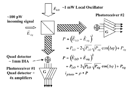
The local oscillator power can be adjusted, according to the required photoreceiver performance. To reduce power consumption, temperature gradients at the optical bench due to hot spots at the photoreceivers, and to provide additional design margin, we aim for a low-noise wide-bandwidth photoreceiver development operating at low levels. Using 0.5 mW local oscillator optical power on the entire quadrant photoreceiver (of the order of 100 W per quadrant), and assuming a responsivity of 0.7 A/W for InGaAs photodiodes at a laser wavelength of 1064 nm, the shot-noise can be computed as
| (2) |
Allocating of the shot-noise level – – to the input current noise contribution of a quadrant photoreceiver, and considering this is the quadrature sum of the current noise of the individual quadrants, we set an input current noise goal of for the single-quadrant photoreceiver transimpedance amplifier (TIA).
II Photodetector transimpedance amplifier
We have chosen a conventional DC-coupled TIA topology with a single ultra-low noise / wide-bandwidth operational amplifier (op-amp), as shown in Figure 2.
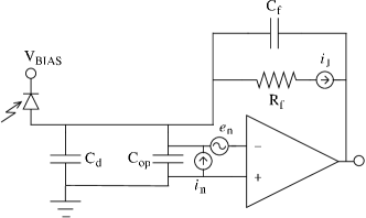
II.1 Noise model
For the TIA topology shown in Figure 2, two main input current noise sources have been identified in the electronics:
-
•
Johnson noise () from feedback resistor :
(3) where is the Boltzmann’s constant, and is the temperature (in Kelvin).
-
•
Op-amp noise properties: The current and voltage noise properties of the op-amp contribute to the total TIA input current noise.
-
–
The op-amp current noise sums directly to the TIA input.
-
–
The op-amp voltage noise translates to current noise at the TIA input over the input and feedback impedances as
(4) where is the frequency, and is the total circuit capacitance
(5) including the photodiode capacitance , feedback impedance , op-amp common-mode input capacitance , and stray capacitances from the board, components and packaging.
-
–
The bandwidth of the photoreceiver can be estimated as
| (6) |
where is the gain-bandwidth product of the operational amplifier. The total TIA input current noise model can be expressed as
| (7) |
where is the normalized TIA transfer function, is a frequency dependent component of the input current noise (see Equation 4), and is the quadrature sum of various contributors that can be approximated by neglecting their frequency dependency for modeling purposes. For example, the expected current noise in the photoreceiver shown in Figure 2, can be computed as
| (8) |
where is the op-amp current noise, is the Johnson noise of the feedback resistor (see Equation 3), and is the shot-noise from the photodiode dark current. It can be seen from Equation 5 that the photodiode capacitance and the op-amp common-mode input capacitance are crucial factors in the total noise budget. The challenge for the photodiode manufacture lays in achieving a minimum capacitance per unit area while maintaining high responsivity and low leakage if reverse-biased. For the TIA electronics, it is necessary to identify an op-amp with minimal common-mode input capacitance, current and voltage noise, and a gain-bandwidth product large enough to maintain the required sensitivity over the required measurement bandwidth of 2–20 MHz.
III Prototype photoreceivers
III.1 Collaboration with industry
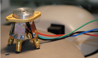
Under a Small Business Innovation Research (SBIR) grant, the company Discovery Semiconductors has developed a large-area quadrant photodiode (QPD) of 1 mm diameter and a quadrant capacitance of 2.5 pF when reverse-biased at 5 V. A first fully integrated quadrant photoreceiver (Figure 3: QPD + TIA electronics) performs with an equivalent input current noise of less than 3.2 pA/ below 20 MHz joshi-2009 . The characteristics of this prototype quadrant photoreceiver are:
-
•
Diameter of 1 mm with a 20 m inter-quadrant gap.
-
•
Individual quadrant capacitance = 2.5 pF when reverse-biased at 5 V.
-
•
Dark current: 140 nA when reverse-biased at 5 V.
-
•
Responsivity at 1064 nm: A/W (quantum efficiency of 0.8).
-
•
TIA characteristics:
-
–
feedback impedance: , .
-
–
op-amp ADA4817: , , = 1.4 pF, .
-
–
Discovery Semiconductors has been awarded a second stage grant to further develop quadrant photoreceivers. Given the successful development of a large-area low-capacitance QPD in the first step, the next stage will be focused on the noise reduction of the electronics, e.g. by integrating op-amps with better noise properties and studying alternative TIA topologies. We expect to receive additional devices with lower noise electronics at a later date.
III.2 Laboratory prototypes
Working in parallel with Discovery Semiconductors to try to understand the noise and bandwidth trade-offs in more detail, we have identified the ultra-low noise / high-bandwidth op-amp EL5135 from Intersil intersil_el5135 with the following nominal noise properties:
, , = 1 pF, .
A significant reduction in the op-amp voltage noise together with the bandwidth enhancement (given by the higher ) were the main factors considered
for selecting the EL5135 for laboratory prototype photoreceivers. Despite the higher op-amp current noise of the EL5135 compared to the
ADA4817 (mentioned above), the lower voltage noise of the EL5135 enables us
to achieve significantly better performance over the entire bandwidth from
2–20 MHz. The penalty is somewhat higher noise at low frequencies. According to Equation 7, the term
(corresponding to the quadrature sum of various current noise contributions,
including the op-amp current noise ) dominates at lower frequencies, while
the frequency dependent term (consisting of the op-amp voltage noise
swing across the total equivalent TIA impedance) becomes the dominant noise
contribution at higher frequencies.
We have designed a TIA with a feedback impedance , , and an expected bandwidth of
40 MHz (according to Equation 6). We have built two different prototype
boards to test the noise properties of a TIA with the EL5135 op-amp:
-
•
GAP500Q photoreceiver board: we have chosen the commercially available QPD GAP500Q from GPD Optoelectronics gpdopto_gap500q with a diameter of 0.5 mm and a responsivity of approximately 0.7 A/W (quantum efficiency of 0.8) at 1064 nm. When reverse-biased at 5 V, this device has a nominal quadrant capacitance = 2.0 pF and a dark current of 2.0 nA, according to the manufacturer. The purpose of this investigation is to operate the TIA electronics with a photodiode that approximates the per-quadrant capacitance and package parasitic capacitance of the larger area Discovery Semiconductors detector.
-
•
Mock-up TIA board: we have built a board for controlled noise investigations of the TIA performance, shown in Figure 4.
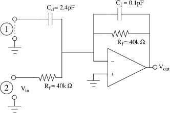
Figure 4: Schematics of TIA mock-up board for noise measurements and frequency response measurements. This board has two inputs:
-
1.
input 1: an input capacitor (2.4 pF) of similar quadrant capacitance is used to replace the photodiode. For noise measurements, this input can be grounded while maintaining input 2 open.
-
2.
input 2: this is used to measure the expected photoreceiver transfer function (TF) by injecting a signal (maintaining input 1 open), and scaling it accordingly by the feedback gain (). The equivalent input current noise can be obtained, by dividing the output voltage noise by the scaled transfer function.
-
1.
The GAP500Q photodiode was reverse-biased with a battery power supply at 5 V, and the op-amps in both circuits were driven with a power supply at 5 V.
IV Performance measurements of prototype photoreceivers
We operated the photoreceiver using only one quadrant of the GAP500Q QPD with the EL5135 op-amp for the TIA electronics. The photoreceiver output voltage noise is given by
| (9) |
where is the photocurrent shot-noise of the incident light, is the photoreceiver transfer function, and is the equivalent input current noise of the TIA electronics. Operating under dark conditions, the photoreceiver output voltage noise is given by
| (10) |
By dividing Equations 9 and 10 diekmann-2008 , we obtain that the input current noise of the TIA electronics can be computed as
| (11) |
For equivalent input current noise measurements, we used a light-emitting diode
(LED) at a center wavelength of 1050 nm (50 nm) thorlabs_led1050e as shot-noise-limited light source.
We measured the GAP500Q photoreceiver output voltage noise with () and
without () LED light, operating at two different optical power levels
of 90 W and 60 W that are representative for the expected nominal
100 W per quadrant. These measurements showed
equivalent input current noise levels that did not scale with the DC
optical power level (90 W and 60 W). This also shows that the
measured current noise upon subtraction of the shot-noise
contribution, is not dependent on the optical power, which is consistent with a shot-noise behavior of the light source.
We also measured the output voltage noise and the transfer function () of our mock-up TIA
board (see Figure 4). Analogous to Equation 10, the
input current noise can be computed by referring the output voltage noise (upon
subtraction in quadrature of the RF spectrum analyzer voltage noise floor) to the input
dividing by the transfer function. Figure 5 shows the noise measurements.
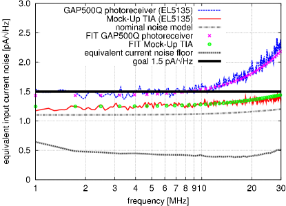
The GAP500Q photoreceiver reaches a level of about up to 10 MHz, increasing at higher frequencies. It exceeds the noise goal by approximately 20% () at 20 MHz. The mock-up TIA circuit meets our noise goal over the entire bandwidth (2-20 MHz), however, it shows noise in excess of the model. At lower frequencies the equivalent input noise is determined by excess current noise (: assumed to have no frequency dependence, Equation 8), while at higher frequencies, the increasing slope is dominated by the op-amp voltage noise swing across the total circuit capacitance (: dependent on frequency, Equation 4). We run a set of measurements in order to determine some of the involved unknowns:
-
1.
op-amp voltage noise (): we measured the op-amp voltage noise on a separate sample of the EL5135, by driving the op-amp as a voltage follower with grounded input. A low-noise 10x amplifier in series with the op-amp output was necessary for a voltage noise measurement above the spectrum analyzer noise floor. The voltage noise level measured was at 10 MHz, which is significantly higher than the specified .
-
2.
photodiode and feedback capacitances (, ): using a LCR-bridge impedance measurement instrument, we measured the photodiode quadrant capacitance on a separate sample of the GAP500Q to be 3.2 pF with a 5 V reversed bias, which is higher than the nominal 2 pF. We also measured the capacitor of the mock-up board and the feedback capacitor to be 2.2 pF (nominally 2.4 pF) and 0.1 pF, respectively.
These noise properties are higher than specified and may account for part of the excess noise. A direct measurement of the op-amp current noise , the op-amp input capacitance , and the stray capacitances of the circuit involve the development of dedicated electronic boards (currently on-going) for well-controlled measurements. These measurements will be conducted at a later stage. However, it is possible to obtain an estimate of these values by fitting them as parameters of the noise model (Equations 7 and 8) to the two measured data sets. The noise level difference (offset) in the data of the GAP500Q photoreceiver and the mock-up TIA is an indicator of a significant excess current noise contribution, , present in the photo-measurement and not in the measurement of the mock-up TIA. This can also be included into the fit by considering the following non-frequency dependent contributions (Equation 8) for each case:
| (12) | |||||
| (13) |
The capacitance values and are assumed to be known from the LCR-bridge measurements. We also assume similar op-amp and board noise properties (, , ) for the two circuits. From the fit, we obtained an op-amp current noise of (about 20% higher than nominal ) and a combined stray plus op-amp input capacitance pF (1 pF nominal ). We also fit a common op-amp voltage noise for the two data sets to be , which is comparable (within ) to the independent measurement (), but about 25% higher than nominal (). Table 1 summarizes the current best estimates (CBE) of the photoreceiver noise properties.
| parameter | nominal | CBE | method |
|---|---|---|---|
| 2.0 | 3.2 | measured | |
| 1.5 | 1.9 | fit | |
| 0.9 | 1.1 | fit | |
| 1.0 | 1.3 | fit | |
| - | 0.7 | fit |
The excess current noise contribution, , present in the GAP500Q photoreceiver data was determined to be of the order of . We have reversed-biased the photodiode with a battery power supply, therefore, noise on the bias voltage translating to excess current noise is not the cause. Additional tests are required to determine the origin of this contribution.
V Conclusions and Outlook
We have presented the results of noise measurements conducted on different photoreceiver prototypes. The measurements showed approximately 20% noise in excess of our goal between 10–20 MHz. Direct measurements of the op-amp voltage noise and the reverse-biased QPD quadrant capacitance evidenced noise levels higher than nominal, accounting for part of the excess noise at higher frequencies. By fitting the parameters of the noise model to the data, we obtained estimates for the combined stray plus op-amp input capacitance and the op-amp current noise , which was determined to be approximately 20% higher than nominal. Significant excess current noise (50% of total) was determined between photoconductive (GAP500Q photoreceiver) and electronic (mock-up TIA) noise measurements. Additional testing is required to determine its origin. The measured photoreceiver performance is of the order of below 10 MHz, increasing up to at 20 MHz with a 3 dB bandwidth of 34 MHz. However, the mock-up TIA performs at a level of below 20 MHz (10% higher than expected from the nominal model) with a measured 3 dB bandwidth of 38 MHz. This suggests a significantly better performance of a real photoreceiver with the current TIA design, depending upon clarification and, if viable, mitigation of the excess current noise . In addition, as following steps, we plan to conduct spatial scanning of the photodiode surfaces, measurement of inter-quadrant cross-talk, and differential wavefront sensing angle measurements.
VI Acknowledgements
This research was supported in part by NASA contract ATFP07-0127. F. Guzmán Cervantes is supported by an appointment to the NASA Postdoctoral Program at the Goddard Space Flight Center, administered by Oak Ridge Associated Universities (ORAU) through a contract with NASA. We thank A. Joshi, S. Datta and J. Rue for stimulating discussions.
References
- (1) Jennrich O, LISA technology and instrumentation, Class. Quantum Grav. 26 (2009).
- (2) Shaddock D, Ware B, Halverson P, Spero R, Klipstein B, Overview of the LISA phasemeter, AIP Conf Proc. 873 654-60 (2006).
- (3) Bykov I, Esteban Delgado J, García Marín A, Heinzel G, Danzmann K, LISA phasemeter development: Advanced prototyping, J. Phys.: Conf. Ser. 154 (2009).
- (4) Joshi A, Rue J, and Datta S, Low-Noise Large-Area Quad Photoreceivers Based on Low-Capacitance Quad InGaAs Photodiodes, IEEE Photonics Technology Letters, Vol.21, No.21 (2009).
- (5) Datasheet of Intersil device EL5135: http://www.intersil.com/data/fn/fn7383.pdf
- (6) Datasheet of GPD Optoelectonics device GAP500Q: http://www.gpd-ir.com/
- (7) Diekmann C, Phasenstabilisierung und -auslesung für LISA, Diploma Thesis, Leibniz Universität Hannover, Germany (2008).
- (8) Datasheet of THORLABS device LED1050E: http://www.thorlabs.com/Thorcat/16300/16388-S01.pdf