Noninvasive Embedding of Single Co Atoms in Ge(111)21 Surfaces
Abstract
We report on a combined scanning tunneling microscopy (STM) and density functional theory (DFT) based investigation of Co atoms on Ge(111)21 surfaces. When deposited on cold surfaces, individual Co atoms have a limited diffusivity on the atomically flat areas and apparently reside on top of the upper -bonded chain rows exclusively. Voltage-dependent STM imaging reveals a highly anisotropic electronic perturbation of the Ge surface surrounding these Co atoms and pronounced one-dimensional confinement along the -bonded chains. DFT calculations reveal that the individual Co atoms are in fact embedded in the Ge surface, where they occupy a quasi-stationary position within the big 7-member Ge ring in between the and atomic Ge layer. The energy needed for the Co atoms to overcome the potential barrier for penetration in the Ge surface is provided by the kinetic energy resulting from the deposition process. DFT calculations further demonstrate that the embedded Co atoms form four covalent Co–Ge bonds, resulting in a Co4+ valence state and a 3 electronic configuration. Calculated STM images are in perfect agreement with the experimental atomic resolution STM images for the broad range of applied tunneling voltages.
pacs:
68.43.Fg, 68.47.Fg, 68.37.Ef, 81.07.TaI Introduction
The continuous miniaturization of electronic circuits has resulted in the emergence of novel classes of nanometer size devices that rely on the quantum-mechanical nature of charge carriers. Bhattacharya et al. (2004); Kuo et al. (2005) Examples of state-of-the-art nanodevices can be found in molecular electronics Whalley et al. (2007); Grigoriev et al. (2006); Parks et al. (2010) and spintronics. Prinz (1995) The dimensions of the active elements, connections and separations are now being reduced to the order of a few atomic rows and, in the ultimate limit, devices may be built up using atomic size elements Haider et al. (2009); Tan et al. (2009) that are connected by atomic nanowires. However, to fulfill the demands related to the never ceasing development of electronics, novel materials with electronic properties superior to that of the currently used silicon are required. Among all candidates germanium is considered as one of the most promising alternative materials Bracht et al. (2009); Wundisch et al. (2009) because it allows higher switching speeds due to a lower effective hole mass and a higher electron and hole drift mobility. Sze and Irvin (1968) This makes germanium ideally suited for use in ultrafast complementary metal-oxide-semiconductor technology, in particular for metal-oxide-semiconductor field-effect transistors Lee et al. (2005); Leitz et al. (2002); Claeys and Simoen (2007) and band-to-band tunneling field-effect transistors. Appenzeller et al. (2004) For this purpose detailed investigations of the electronic properties of dopants/defects or metal alloys in Ge crystals are obviously required. Chui et al. (2003)
One of the major challenges for future nanoelectronic applications is the controlled preparation of low-dimensional structures on semiconductor surfaces, e.g. quantum dots Reimann and Manninen (2002) and quantum wires. Nilius et al. (2002); Wang et al. (2004); Schouteden et al. (2009) Due to their broad range of electronic and magnetic properties, such nanostructures are ideal model systems for the fundamental study of low-dimensional physics as well as for the exploration of new device concepts Kouwenhoven et al. (2001) that also exploit the spin character of the charge carriers. Prinz (1995); Wolf et al. (2001); Žutić et al. (2004)
Within this context, deposition of metal atoms on Ge surfaces has attracted considerable scientific interest during recent years, since it was found that atoms of different materials self-organize into different types of nanostructures after deposition on Ge. It has been demonstrated that deposited Mn atoms do not coagulate on Ge(111)c28 surfaces in the initial adsorption stage, yielding zero-dimensional (0D) structures on Ge(111). Zeng et al. (2004); Profeta et al. (2004) On the other hand, Pt, Oncel et al. (2005); Schäfer et al. (2006); Stekolnikov et al. (2008a, b); Vanpoucke and Brocks (2010) Au Sauer et al. (2010); van Houselt et al. (2008) and Sn atoms Tomatsu et al. (1007) spontaneously form one-dimensional (1D) atomic chains on Ge(001), whereas Pd Fischer et al. (2007, 2007); Wang et al. (2006) and Ag Lince et al. (1983); Chan and Altman (2002) atoms favor the formation of two-dimensional (2D) or three-dimensional (3D) particles on Ge(001).
The emerging field of spintronics requires (self)assembly of nanostructures with well-defined magnetic properties on semiconducting surfaces. Due to the high spin polarization of the charge carriers near the Fermi level, Co is one of the most important elements used in magnetic recording media as well as in giant magnetoresistance devices. Parkin (1993) Recently, the electronic and magnetic behavior of ultrathin ( monolayers) Co/Ge Tsay et al. (2002); Ryan et al. (2004); Tsay et al. (2004a, 2005); Chang et al. (2006) and Co/Ag/Ge Tsay et al. (2003, 2004b); Su et al. (2006) films has been investigated. The initial adsorption stage of single Co atoms on Ge surfaces has not been studied so far. Thorough knowledge of the formation process of the Co/Ge interface during the first adsorption stages is, however, of crucial technological and fundamental interest.
Here, we present a comprehensive study of the initial growth stages of Co on 21 reconstructed Ge(111) by means of low-temperature (LT) scanning tunneling microscopy (STM) and spectroscopy (STS), combined with first-principles density functional theory (DFT) calculations within the local-density approximation. STM and STS are ideal tools to investigate with high spatial and energy resolution the surface reconstruction and the local electronic properties of the Ge(111) surface after adsorption of individual Co atoms. DFT calculations on the other hand allow us to predict the electronic properties of systems of up to thousands of atoms in size. High resolution STM/STS combined with DFT hence provides a powerful tool for the investigation of atomic size systems. Here, we report on the first experimental observation of “noninvasive embedding” (i.e. without destroying the surface reconstruction) of individual Co atoms in the Ge(111)21 surface and on the formation of larger Co/Ge intermixed layers after Co deposition on the cold () Ge(111)21 surface. The location of an individual Co atom in the Ge surface, its influence on the surrounding Ge atoms and the resulting electronic properties are systematically investigated. Voltage-dependent STM imaging reveals a highly anisotropic electronic perturbation of the Ge surface surrounding the Co atom, which is accompanied by pronounced 1D confinement along the -bonded chains. Our experimental findings are well explained by the detailed DFT calculations.
II Instrumentation
STM and STS measurements were performed with a LT STM setup (Omicron Nanotechnology), operating at a base pressure in the range. All data are acquired at . Electrochemically etched W tips were cleaned in situ by repeated flashing well above to remove the surface oxide layer and any additional contamination. The tip quality was routinely checked by acquiring atomic resolution images of the “herringbone” reconstruction of the Au(111) surface. Barth et al. (1990); Schouteden et al. (2008) STM topographic imaging was performed in constant current mode. The tunneling voltages indicated in the text and figure captions are with respect to the sample (the STM tip is virtually grounded). Image processing was performed by Nanotec WSxM. Horcas et al. (2007)
Ge single crystals with a resistivity of are doped with Ga at a doping level of to , resulting in -type bulk conductivity. Ge bars, with their long axis aligned with the (111) direction, were cleaved in situ at room temperature in the sample preparation chamber at a pressure of around . The freshly cleaved samples were transferred within about 5 minutes to the STM measurement chamber. The pressure in the STM measurement chamber was about during the LT STM measurements. Under these conditions the cleaved Ge surfaces were observed to retain their cleanliness for 5 to 7 days. This way, we have investigated 7 freshly cleaved Ge(111) crystals.
After checking the freshly cleaved Ge(111)21 sample in the STM measurement chamber, monolayers of Co are deposited on the cold Ge(111)21 surface () in the sample preparation chamber. Deposition was achieved by evaporation from a high purity Co (99.9996%) rod with an e-beam evaporator, at pressures below and at a low deposition rate of around monolayers (MLs) per seconds. After Co deposition, the Ge(111)21 sample is transferred immediately to the LT STM measurement chamber. Overall transport time, including deposition time, was around . Here we focus on the results obtained on 4 different Co/Ge(111)21 samples for which atomic resolution STM topography images were recorded and analyzed.
III Experimental Results
III.1 Topography and electronic structure of the freshly cleaved Ge(111)21 surface
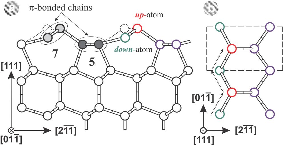
The 21 reconstruction of the Ge(111) surface consists of -bonded chains of Ge atoms running in the direction. Pandey (1981); Northrup and Cohen (1983); Feenstra and Slavin (1991) Only every other (upper chain) row can be imaged by STM. Feenstra et al. (2001) The surface unit cell contains two atoms, both having one dangling bond. This dangling bond is responsible for -bonding along the upper surface chain rows (see Fig. 1). In the original Pandey geometry, Pandey (1981) the two upper atoms of the 7-member ring have the same height and form “zigzag” chains along the direction. However, due to buckling, one of these two atoms (up-atom) is shifted upwards (out of the surface) while the other (down-atom) is shifted downwards (into the surface), as illustrated in Fig. 1. The occupied surface states are mainly localized on the up-atom, while the empty surface states are mainly localized on the down-atom. Consequently, the bonding surface states band derived from the up-atom orbital is filled, while the anti-bonding surface states band derived from the down-atom orbital is empty.
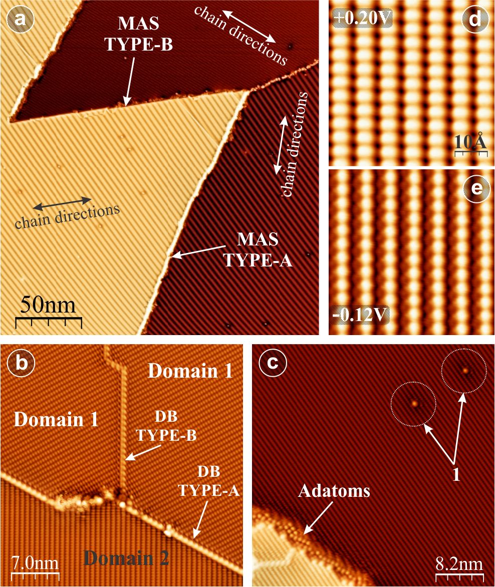
In Fig. 2 we present typical large scale [(a)-(c)] and high resolution [(d)-(e)] STM topography images of the clean Ge(111)21 surface. Large atomically flat terraces up to can be observed, which are separated from each other by monatomic steps (MASs). It can be observed in Fig. 2 (b) that the Ge(111)21 surface consists of different types of domains with slightly different atomic arrangement. Einaga et al. (1998) This is related to the threefold rotational symmetry of the surface. The domains are found to be separated by two different types of domain boundaries (DBs) [see Fig. 2 (b)]. At the first type of DB, referred to as a type-A DB following the terminology used in Ref. [Einaga et al., 1998], the atomic rows at the opposite sides of the DB are rotated by an angle . The second type DB, the so-called anti-phase DB or type-B DB, [Einaga et al., 1998] is formed due to a shift of the -bonded chain rows in the direction by half a unit cell. We found that most DBs are of type-B and that the type-A DBs often exhibit (local) disorder. Muzychenko et al. (2010)
In addition, two types of MASs can be observed [see Figs. 2 (a) and (c)]. With respect to the upper terrace one type of MASs, hereafter referred to as type-A, is oblique to the -bonded chain rows on the terrace. The second type of MASs, hereafter referred to as type-B, is parallel to the -bonded chain rows. One should note that Fig. 2 (a) exhibits pronounced Moiré fringes that run along one direction and become visible because of the large size of the image, Guo et al. (2004) while the -bonded chain rows are not visible on the STM image and their direction is specified by arrows for each of the terraces. We find that Ge adatoms are often present at the MASs, both on the upper and on the lower terrace, except on the upper terrace of type-A MASs. At these terraces the surface is either locally distorted or a 24 or c28 surface reconstruction occurs [Fig. 2 (c)]. Feenstra and Slavin (1991) The Ge surface adatoms are probably created upon cleavage at room temperature, after which the adatoms can migrate along -bonded chain rows to the MAS regions. Furthermore, (individual) Ge adatoms can be frequently observed on atomically flat Ge(111)21 terraces as well above a charged subsurface Ga impurity [see label (1) in Fig. 2 (c)]. These adatoms are well separated from each other and their number is in good agreement with the low doping level of our Ge samples.
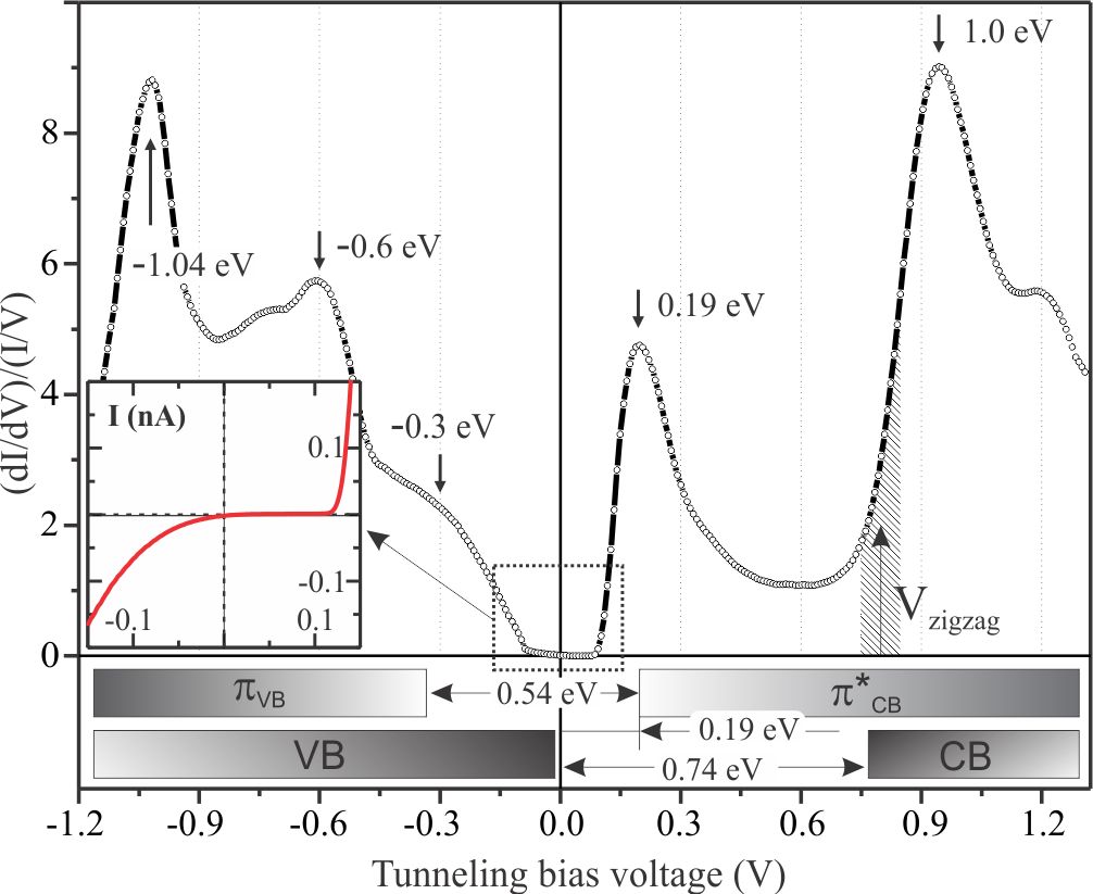
In Fig. 3 we present a typical normalized conductance spectrum recorded at the p-type Ge(111)21 surface. The main energy bands are indicated by gray rectangles at the bottom of Fig. 3. In the spectrum the large peak around can be assigned to the onset of the unoccupied surface states conduction band related to the upper -bonded chains of the Ge(111)21 surface (see Fig. 1). Bechstedt et al. (2001); Kobayashi (2003) Two energy gaps can be discerned: A narrow gap of about and a wide gap of about . The latter corresponds to the forbidden energy gap of the projected bulk band structure of the Ge(111) surface at low temperature. On the other hand, the narrow gap corresponds to the energy gap between the filled bulk valence band (VB) and the unoccupied surface states conduction band (). Using STS Feenstra et al. (2001) as well as photoemission experiments, Nicholls et al. (1983, 1984, 1985) the surface states band gap has been determined before, yielding a gap value of . From Fig. 3 it can be concluded that the high resolution STM images in Fig. 2 (e) and Fig. 2 (d) were obtained at tunneling voltages near the top of VB and the bottom of , respectively.
III.2 Adsorption of Co atoms on Ge(111)21
In Figs. 4 (a) and (b) we present two typical large scale STM topography images of the Ge(111)21 surface after Co atom deposition corresponding to a coverage of 0.032 ML. Three different kinds of structures are formed after Co deposition: (i) Co/Ge intermixing layers (ILs) [indicated by the two arrows with label 1 in Fig. 4 (a)], (ii) Co clusters consisting of multiple Co atoms [indicated by the two arrows with label 2 in Fig. 4 (b)] and (iii) well separated individual Co atoms [indicated by the two arrows with label 3 in Fig. 4 (b)].
The Co/Ge ILs are formed due to the consecutive accumulation of Co atoms at surface/subsurface defects, e.g. DBs and MASs. Muzychenko et al. (2011) As indicated by the results of our DFT calculations that are presented below, Co atoms are able to migrate along the -bonded chain rows, despite the low temperature of the sample during Co deposition (). Co/Ge ILs are found both on the upper and lower terraces at type-A MASs. At the type-B MASs, formation of a Co/Ge IL occurs only on the lower terrace. Near DBs Co/Ge ILs are observed on both sides of the type-A and type-B DBs. Co/Ge ILs can be found on atomically flat terraces as well, far away from any DBs and MASs. Since Co free atomic size defects, including in particular Ga subsurface impurities, Muzychenko et al. (2010) can no longer be observed after Co deposition, this suggest that these defects act as nucleation centers for the formation of Co/Ge ILs. The amount of Co/Ge ILs formed on atomically flat terraces roughly scales with the amount of atomic scale defects that is observed prior Co deposition. A more detailed discussion on the formation of Co/Ge ILs will be presented elsewhere. Muzychenko et al. (2011)
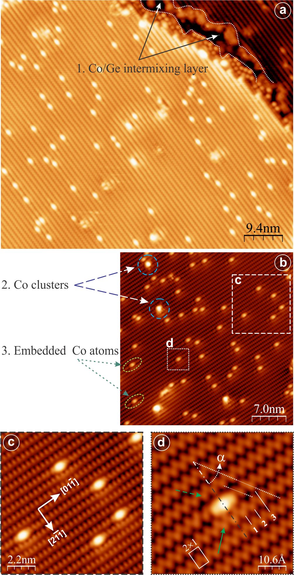
Only a small fraction of the Co atoms coagulates into small Co clusters. A larger fraction of the Co atoms remains under the form of individual atoms after deposition. At tunneling voltages above these individual atoms appear as bright protrusions located on the upper -bonded chain rows. At other tunneling voltages the Co atoms are observed differently. This voltage dependence is discussed in more detail in Section III.3 below. High resolution STM topography images of individual Co atoms are presented in Figs. 4 (c) and (d). The amount of individual Co atoms that can be inferred from Figs. 4 (a) and (b) is . % of the deposited amount of Co atoms is observed as individual Co atoms, while % contributes to the formation of Co/Ge ILs and Co clusters. It is important to already note here that the individual Co atoms are actually not on top of the Ge surface, as will be demonstrated in detail in Section IV below by comparing the experimental STM images to simulated STM images based on DFT calculations. According to the DFT calculations, individual Co atoms penetrate into the Ge surface and reside in between the and the atomic layer (AL), in a quasi-stable position (at low temperatures) inside the 7-member Ge ring of the 21 reconstruction (see Fig. 1). This “embedding” is found to influence the local electronic structure, but does not give rise to a modified surface reconstruction, as can be seen in Figs. 4 (c) and (d). We therefore refer to this embedding as “noninvasive”.
The low temperature of the Ge substrate during Co deposition appears to be crucial for obtaining individual, well separated Co atoms. As mentioned above, in spite of the low substrate temperature, the larger fraction (around %) of the Co atoms still exhibits sufficient surface mobility to migrate to defects where Co/Ge ILs are formed [see Fig. 4 (a)]. The residual fraction of deposited Co atoms (around %) remains confined to defect free atomically flat terraces of the 21 surface. Recently, we reported that these Co atoms diffuse from their quasi-stable sites to surface/subsurface defects as well after warming up the sample to room temperature. Muzychenko et al. (2011) However, as long as the sample remains at low temperatures, the embedded individual Co atoms remain immobile during the experiments in the investigated voltage range.
As illustrated in Fig. 4 (d), the “zigzag” structure of the 21 reconstruction of the low doped p-type Ge(111) surface (see Fig. 1) becomes observable for a limited range of tunneling voltages . From Fig. 3 we can conclude that both the unoccupied surface states (wave functions that are mainly localized on the down-atoms) and the unoccupied states at the bottom of conduction band (CB) (wave functions which are partially localized on the up-atoms Nie et al. (2004)) become available for tunneling within this voltage range. Although the wave functions on the up-atoms have a smaller amplitude, the higher position of these atoms implies that they appear more prominently in the STM images than the down-atoms when the applied tunneling voltage increases. Within the voltage range (this range is marked by the gray dashed area in Fig. 3), the contribution of to the tunneling current remains nearly constant, while the contribution from CB rapidly increases with increasing up to . Hence, a balance exists between tunneling into up- and down-atoms within the voltage range, which implies that both the up- and down-atoms of the -bonded chain rows are visualized in constant-current STM images [see Fig. 4 (d)]. We found that the precise value of depends on the doping level as well as on the semiconductor type. E.g., the 21 reconstruction of the (111) surface of heavily doped n-type Ge(111) (phosphorus doping level ) reveals zigzag chains around . Previously, it has been reported by Trapmann et al. that zigzag chains appear around for n-type Si(111)21 surfaces. Trappmann et al. (1999) The precise value of is therefore a characteristic feature of the semiconductor surface under investigation.
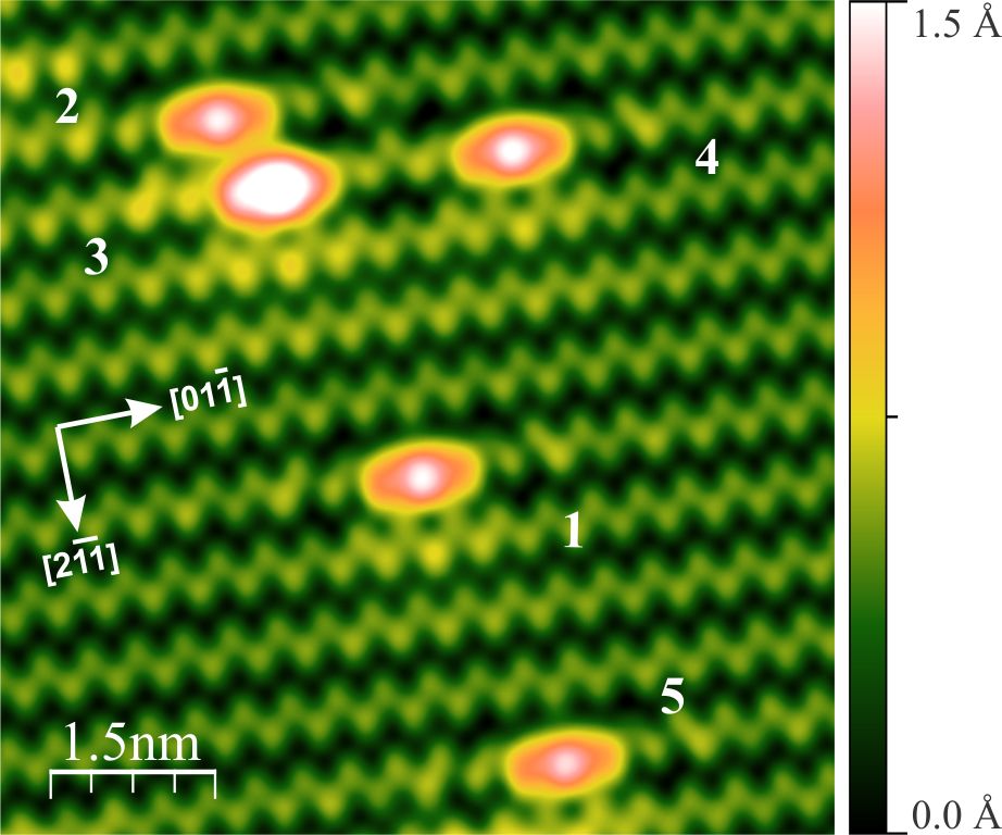
From Figs. 4 (a)-(d) it becomes clear that all individual Co atoms occupy identical positions at the Ge surface: Their appearance is symmetric with respect to the direction [the symmetry axis is drawn as a black dash-dotted line in Fig. 4 (d)], while they appear asymmetric with respect to the direction. The latter can be related to the asymmetry of the 21 surface reconstruction (due to buckling) along this direction. The relevant crystallographic directions are indicated in Fig. 4 (c) and are the same for Figs. 4 (b) and (d). The symmetry and asymmetry of the Co atoms with respect to the and directions, respectively, becomes most clearly resolved for tunneling voltages near [see Fig. 4 (d) and Fig. 5]. The bright protrusion related to an individual Co atom occupies about 2 surface unit cells along the -bonded chain rows. Moreover, in Fig. 4 (d), disturbance of the zigzag atomic structure along the direction can be observed near the Co atom over a distance unit cell periods. In Fig. 4 (d) the edge of the unperturbed zigzag -bonded chain on the right hand side of the Co atom is marked by a long dotted white line, forming an angle with the symmetry axis. Closer to the Co atom related protrusion, a brighter/higher feature [marked by the short dotted white line and indicated by the label 2 in Fig. 4 (d)] is visible, also making an angle close to with the symmetry axis. The same disturbance is observed to the left of the Co atom (mirror symmetry with respect to the direction). Identical characteristic features are observed for all investigated individual Co atoms on differently oriented Ge(111)21 domains.
In addition to the disturbance of the zigzag structure, an asymmetry of the electronic structure of the neighboring -bonded chain rows (with respect to the direction) near an embedded Co atom is observed. This asymmetry is most clearly resolved in maps of the local density of states (LDOS) (not shown here). It can be observed as well in STM topography images around : The lower -bonded chain row in Fig. 4 (d) (indicated by the green solid arrow) appears brighter when compared to subsequent rows, while the upper -bonded chain row (indicated by the green dashed arrow) does not appear to be influenced by the embedded Co atom. This asymmetric perturbation and the disturbance of the zigzag structure of the -bonded chain rows always occur simultaneously and were observed with various STM tips. Figure 5 presents an STM topography image of 5 embedded single Co atoms that all induce a similar difference between the Co neighbor chains. As we will demonstrate below when discussing the results of our DFT calculations, this additional asymmetry of the Ge(111)21 surface induced by the Co atoms allows us to determine the crystallographic direction of the different Ge(111)21 domains, leading to the conclusion that all investigated Ge(111)21 surfaces consist of domains with -bonded chain-left isomers (negative buckling) exclusively.
There appears no significant electronic interaction between two embedded single Co atoms that reside in the same -bonded chain row in close vicinity (down to a distance of 3 unit cells along the direction) in the investigated voltage range from [see Figs. 4 (a) and (b), as well as Co atoms (3) and (4) in Fig. 5]. On the other hand, an electronic interaction effect can be observed for Co atoms that reside in neighboring -bonded chain rows at a distance (in the -bonded chain row direction) smaller than 3 unit cells. This is illustrated in Fig. 5. Indeed, the lower Co atom (3), which is located on a -bonded chain row that is perturbed by the upper Co atom (2), exhibits modified electronic properties. More precisely, Co atom (3) appears more bright in Fig. 5, while Co atom (2) appears similar to the other Co atoms. Note that the modified electronic properties of Co atom (3) are caused by Co atom (2) only and are not related to presence of the neighboring Co atom (4) that is located in the same -bonded chain row.
III.3 Voltage dependent STM investigation of single Co atoms embedded in Ge(111)21
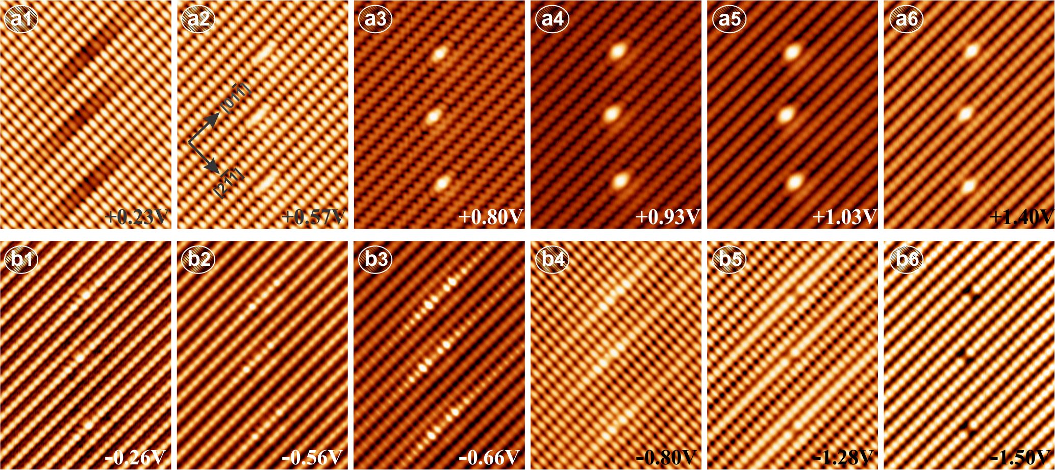
In this section we focus on the novel Co induced electronic features by careful comparison to the electronic properties of the clean Ge(111)21 surface (see Section III.1). First of all it must be noted that deposition of (a small amount of) Co atoms does not change the electronic properties of the defect free Ge(111)21 surface: The characteristic peaks in the STS spectra of the clean Ge(111) surface prior to Co deposition (Fig. 3) are still observed at the 21 reconstructed surface after Co deposition. Figure 6 presents a series of (a) empty and (b) filled states STM topography images of 3 individual, well separated Co atoms embedded in the reconstructed Ge(111)21 surface. Images are recorded at the same location and with the same tip for a broad range of tunneling voltages between and . The series of images reveals a pronounced voltage dependence for both the clean p-Ge(111)21 surface and the electronic influence of the embedded Co atoms on the -bonded chain rows.
In the empty state regime, at high voltages above [Figs. 6 (a5) and (a6)], topography is dominated by the reconstruction lines of the -bonded chain rows in the direction. Individual Co atoms appear as bright protrusions, located directly on the upper -bonded chain row and extending over 2 unit cells of the 21 reconstruction. Maximum contrast of the Co related features is observed around and above this voltage the contrast again decreases. This is because the contribution of the surface states to the tunneling current remains approximately constant, while the contribution of the bulk CB states increases with increasing tunneling voltage (see Fig. 3). At lower voltages around [Fig. 6 (a3)] the zigzag atomic structure discussed above emerges. Around contrast of the Ge atomic corrugation and the Co related protrusions become similar and Co atoms can mainly be discerned by the locally induced perturbation of the 21 surface reconstruction [Fig. 6 (a2)]. In the empty states regime below [Figs. 6 (a1) and (a2)] extra corrugation appears in the STM topography along the direction. Close to the Fermi level the strength of this extra corrugation along the direction becomes comparable to the corrugation along the direction [Fig. 6 (a1), also see Fig. 2 (d)]. Co atoms appear as centro-symmetric striped depressions along the -bonded chain rows. These depressions exhibit a local minimum directly above the embedded Co atom and gradually fade away with increasing distance (up to ) from the local minimum [Fig. 6 (a1)].
In the filled states regime, at voltages close to , topography is again dominated by corrugation of the -bonded chain rows [Fig. 6 (b1), also see Fig. 2 (e)]. Maxima of the atomic corrugation are related to the highest filled bulk VB states that are localized on the Ge up-atoms (see Fig. 1). Co atoms appear as bright protrusions located on the -bonded chain rows [Fig. 6 (b1)]. Below extra corrugation emerges along the direction [Fig. 6 (b4)] and persists down to around . Below topography becomes again completely dominated by the -bonded chain rows along the direction [Fig. 6 (b6)]. Here, Co atoms appear as atomic size vacancies in the upper -bonded chain rows of the 21 surface reconstruction [Figs. 6 (b5) and (b6)].
It is clear from Figs. 6 (a1) and (b2)-(b5) that the embedded Co atom induces a localized 1D perturbation of the LDOS along the -bonded chain rows. STM images recorded with a tunneling voltage near the edge of the surface states bands reveal highly anisotropic scattering of electrons and screening effects with 1D confinement to the -bonded chains. 1D perturbations have previously been reported for Si(111)21 Trappmann et al. (1999); Garleff et al. (2005, 2007) and Ge(111)21 Muzychenko et al. (2010) surfaces. Here, the perturbation near the atomic size defect has a pronounced 1D shape Trappmann et al. (1999) and extends up to along the -bonded chain rows, while the width of the perturbation remains limited to one period () of the 21 reconstruction in the direction. In the empty states regime, the 1D screening effects appear as depressions and become most pronounced near , corresponding to the bottom of the surface states band [Fig. 6 (a1)]. In the filled states regime, the 1D electron scattering effects are observed as protrusions and are most clearly seen near , corresponding to the top of the surface states band [Fig. 6 (b3)]. In both regimes the 1D perturbations exhibit identical mirror-like symmetry with respect to the direction, similar to our recent observations for atomic size surface impurities on Ge(111). Muzychenko et al. (2010)
In summary, we can state that individual Co atoms embedded in Ge(111)21 surfaces exhibit the following general properties:
-
•
Individual Co atoms penetrate into the cold () Ge(111)21 surface after deposition (see Section IV below for more details);
-
•
the 21 reconstruction is preserved after the noninvasive embedding of a Co atom;
-
•
the embedded Co atoms occupy identical positions in the Ge(111) surface and exhibit an identical voltage dependence of the STM topography images;
-
•
the embedded Co atoms exhibit a clear symmetry with respect to the direction, while they exhibit a clear asymmetry with respect to the direction;
-
•
the embedded Co atoms induce highly anisotropic scattering of electrons, which is accompanied by screening effects with 1D confinement along the -bonded chain rows.
IV Discussion and comparison with DFT calculations
IV.1 DFT model of the Ge(111)21 surface
The 21 reconstruction of cleaved Si and Ge (111) surfaces Himpsel et al. (1984); Tromp et al. (1984); Alerhand et al. (1985); Northrup et al. (1991); Feenstra and Slavin (1991) is well described by the commonly used Pandey -bonded chain model described above. Pandey (1981) The Pandey chain geometry leads to a strong coupling of the dangling-bond orbitals along the chain, while the coupling between the chains is much weaker. This geometry does not take into account the effects of buckling, so that the two uppermost surface Ge atoms in the 7-member rings are at the same height. Pandey (1981) Northrup et al. predicted buckling of the two uppermost atoms by about Å (see Fig. 1). Northrup and Cohen (1983) This buckling further reduces the surface energy of the system, yielding two different isomers commonly referred to as -bonded “chain-left” and “chain-right” isomers Takeuchi et al. (1991) (see Fig. 7). Relying on first principle calculations within the computational accuracy that could be achieved at that time (1991), it was found that the chain-left isomer is per surface cell lower in energy when compared to the chain-right isomer. It has been confirmed theoretically Rohlfing et al. (2000) and experimentally Hirayama et al. (2000); Nie et al. (2004) that the chain-left isomer is indeed the dominant isomer at the Ge(111)21 surface. However, because of the very small energy difference between the two different isomers, coexistence of both surface reconstructions and hence the possible existence of Ge(111)21 multi-domain surfaces cannot be totally excluded.
Our theoretical investigation of the noninvasive embedding of Co atoms in the Ge(111)21 surface was performed based on DFT Kohn and Sham (1965) within the local density approximation (LDA). Perdew and Zunger (1981) Calculations were performed with the SIESTA package, Ordejón et al. (1996); Sánchez-Portal et al. (1997); Soler et al. (2002) which relies on the expansion of the Kohn-Sham orbitals by linear combination of pseudo-atomic orbitals. In all calculations a double-zeta basis set with polarization was used. The core electrons were implicitly treated by using norm-conserving Trouiller-Martins pseudopotentials Troullier and Martins (1991) with the following electronic configuration of the elements: H , Ge (Ar ) and Co (Ar) , where the core configurations are indicated between parentheses. A cutoff energy of was introduced for the grid integration, ensuring convergence of the total energy of the system within typically .
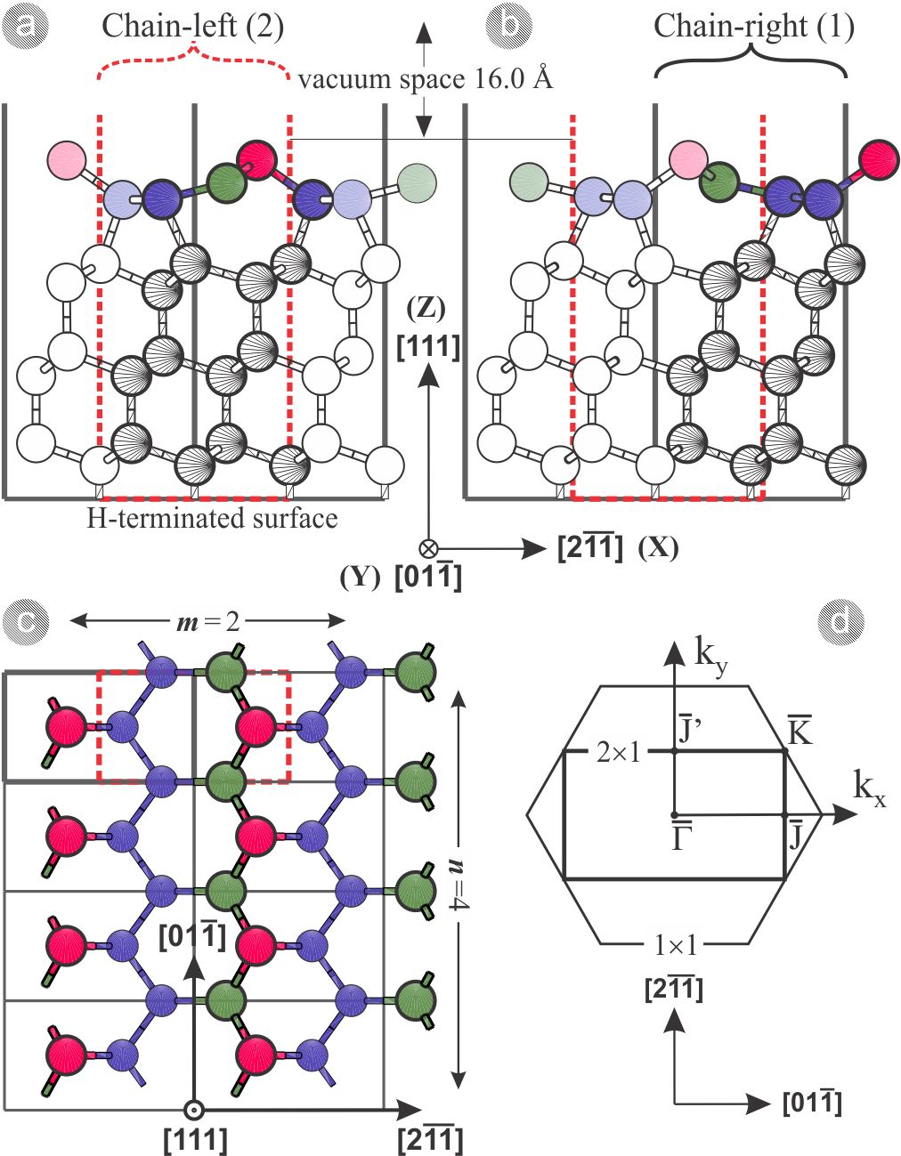
Our calculations are performed in three stages. First, we determine the surface equilibrium geometry for the chain-left and chain-right isomers within one surface unit cell (SUC) using conjugate gradient (CG) geometry optimization. Second, based on the Ge(111)21 SUC, a new supercell (SC) with one Co atom above the surface is constructed and the equilibrium configurations of Co/Ge(111)21 are determined relying on CG geometry optimization. Third, the electronic structure of a still larger SC is calculated, which is then used to perform the DFT based STM topography image simulations.
In order to model the Ge(111)21 surface, a reduced square SUC (unreconstructed) with () lattice vectors is used (Å is half the optimized bulk Ge lattice constant). This SUC consists of a slab of 26 Ge atomic layers, of which one atomic layer is saturated by hydrogen atoms (52 Ge atoms and 2 H atoms per SUC). In the CG geometry optimization the 14 topmost atomic Ge layers are allowed to move, while the 12 layers of Ge and H atoms are frozen at the ideal (bulk) positions. Using 130 k-points within the surface Brillouin zone, the atoms are relaxed until all atomic forces acting on the released atoms are smaller than Å, and the remaining numerical error in the total energy is smaller than for each optimization step.
The final positions of the 9 topmost Ge layers yielding the Ge(111)21 surface reconstruction are presented in Figs. 7 (a) and (c) (chain-left isomers) and Fig. 7 (b) (chain-right isomers). The coordinates of the Ge atoms below the atomic layer are found to change only slightly during the CG geometry optimization. For the considered SUC the two different Ge isomers are both possible for the formation of the 21 reconstruction. Depending on the initial conditions, either the 5-member or the 7-member Ge ring of the reconstruction is present in the 21 SUC. This is illustrated in Figs. 7 (a) and (c) for the chain-left isomer. The black solid bars in Figs. 7 (a) and (c) comprise the 5-member ring SUC, while the red dashed bars comprise the 7-member ring SUC. The same can be done for the chain-right isomer, as illustrated in Fig. 7 (b). For the 5-member ring the upper -bonded chain rows are formed at the joint of the SUC in the direction and are referred to as “chain-left/right (1)” hereafter [see, e.g., the solid colored atoms in Fig 7 (b)]. For the 7-member ring, the upper -bonded chain rows are formed inside the SUC and are referred to as “chain-left/right (2)” hereafter [see, e.g., the solid colored atoms in Fig 7 (a)]. We verified that the chain-left/right (1) and chain-left/right (2) selection exhibit identical electronic properties for periodical boundary conditions. Depending on the position of the adsorbed Co atom with respect to the upper -bonded chain rows in the SC, selection (1) or (2) was chosen. Buckling distances of the chain-left and chain-right isomers are Å, and - Å, respectively. The chain-right isomer has a total surface energy that is higher than the total surface energy of the chain-left isomer, implying that the chain-left isomer should be the dominant isomer for the Ge(111)21 surface. Hirayama et al. (2000); Rohlfing et al. (2000); Nie et al. (2004)
IV.2 Co adsorption sites and energy decomposition
To model the adsorption of a Co atom on the Ge(111)21 surface, we used the 9 topmost relaxed Ge layers for the chain-left and the chain-right isomer that were obtained following the procedure described above (also see Fig. 7). 6 of these 9 atomic layers are allowed to relax. The bottom side of the 3 fixed atomic layers is saturated by hydrogen atoms (16 Ge atoms and 2 H atoms per SUC; Å slab vacuum space separation).
Geometry optimization was carried out for an enlarged 42 SC for both the chain-left and the chain-right isomers. In Fig. 7 (c) we show the three topmost layers of the 42 SC (size is , consisting of 145 atoms) for the chain-left (1) isomer geometry. A Co atom was then located in front of the Ge(111)21 surface. Next, the relaxation of the Co atom was calculated by means of CG geometry optimization. CG geometry optimization for the 42 SC was carried out until all atomic forces acting on the released Co and Ge atoms were below and until the numerical error on the total energy was smaller than per SC for each optimization step. Using a variety of starting coordinates for the Co atom, multiple Co/Ge quasi-stable geometries were tested and their total energies were compared. Both chain-left and chain-right isomer geometries were used. In both cases multiple quasi-stable Co atom sites (with respect to an atomic force tolerance Å) were found, including sites on the Ge(111)21 surface as well as underneath the Ge(111)21 surface, i.e., inside the big 7-member Ge ring. The subsurface sites were identified by using a location inside the 7-member ring as the starting location for the CG geometry optimization. On the other hand, the surface sites were identified by using an initial Co location above the Ge(111)21 surface, at heights in the 3 to range and at various initial coordinates in the ()-plane. This way, 9 quasi-stable sites were identified for the chain-left isomer, of which 6 are located on the Ge surface and 3 are located inside the 7-member ring underneath the Ge surface. For the chain-right isomer 5 surface and 3 subsurface quasi-stable sites were identified.
| Co site number | 42 SC | 84 SC | 144 SC |
|---|---|---|---|
| (1) | moves to site (2) | - | |
| (2) | |||
| (3) | |||
| (4) | |||
| (5) | - | ||
| (6) | |||
| (7) | |||
| (8) | |||
| (9) |
In Table 1 we present for the chain-left isomer geometry and for all possible quasi-stable Co atom sites (labeled (1) to (9) in the first column) an overview of the calculated difference in total energy with respect to the total energy for the Co atom located at site (7). For a 42 SC size (second column) the minimum energy was found to occur for the Co atom located at site (7). Similar calculations were performed for the chain-right isomer geometry and for a 42 SC (data not shown). Again, the minimum energy was found for the case of a Co atom located inside the 7-member ring, but with somewhat lower energy gain when compared to the chain-left geometry.
In order to reduce the influence (related to the periodic boundary conditions) of the restructuring induced by the Co atom within a 42 SC, similar calculations were performed for a 84 SC (size is , consisting of 577 atoms). The obtained values for the difference in total energy for all possible quasi-stable Co atom sites after CG geometry optimization are listed in the third column of Table 1. Similar to the case of the 42 SC, the energy difference is again with respect to the total energy for the Co atom at site (7). When using this larger SC, a transition of the Co atom was found from site (1) to site (2). Also, site (9) was found to be energetically more favorable than site (2) when compared to the 42 SC. This can be explained by the occurrence of longer-range surface relaxations inside the larger SC. Remarkably, for the 84 and 144 SCs all Co sites inside the 7-member ring have a lower energy (see Table 1) with respect to the other sites, which is different from the 42 SC.
Finally, calculated energy values for a 144 SC (size is , consisting of 1009 atoms) are presented for the chain-left isomer geometry in the fourth column of Table 1. Similar calculations were performed for the chain-right isomer geometry (data not shown) and yielded nearly identical results, with again a somewhat lower energy gain with respect to the other sites when compared to the chain-left geometry.
IV.3 Prime location of the Co atom into Ge(111)21 surface
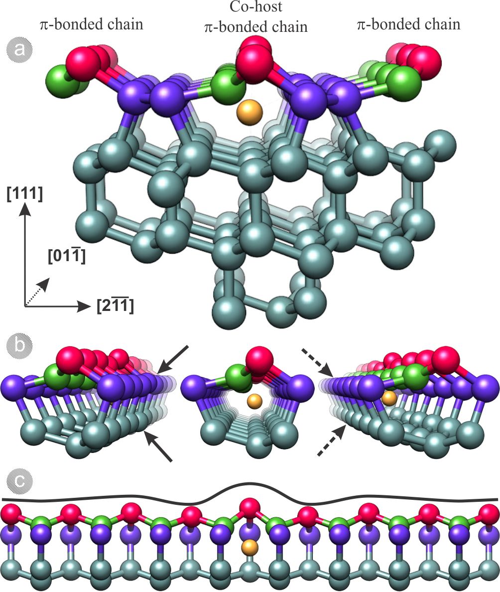
In Fig. 8 (a) we present a 3D ball-and-stick model view of the relaxed Ge(111)21 surface, obtained for the 84 SC with chain-left isomer geometry. The Co atom is located at the site of minimum energy, i.e. site (7) (see third column in Table 1). A 3D front view and a side view of the Co atom inside the 7-member ring are presented in Fig. 8 (b) and in Fig. 8 (c), respectively. Relaxation of the surface Ge up-atoms and down-atoms upon Co atom incorporation can be clearly observed. The black solid envelope line in Fig. 8 (c) reflects the variation of the z-coordinate of the center of the Ge up-atoms (magnified by a factor 2 for clarity). The upward shift of the Ge up-atom located directly above the Co atom is Å, while the downward shift of the neighboring Ge up-atoms is Å. The Co induced shift of the z-coordinate of the Ge up- and down-atoms extends as far as periods along the -bonded chain row of the 21 reconstruction, in agreement with our experimental observations [see Fig. 4 (d) and the related discussion in Section III.2].
The black solid arrows in Fig. 8 (b) (left image) indicate the bulk Ge atoms that experienced the most significant shift of their positions upon embedding of the Co atom. In Fig. 8 (b) (right image) it can be seen that the Ge atoms to the left of the Co atom (indicated by the black dashed arrows) remain unperturbed. This asymmetry of the geometry (and hence of the local electronic properties) of the Co/Ge(111)21 system along the direction is in agreement with our experimental observations: The STM topography images in Fig. 4 (d) and Fig. 5 also exhibit an asymmetry with respect to the direction around an embedded Co atom. Finally, we want to stress once more that the embedding of Co atoms does not give rise to a novel Ge surface reconstruction. Instead, the Ge atoms surrounding the Co atoms experience only small changes of their positions, which is accompanied by changes of the local electronic properties as well. Experimentally, we also found that the 21 reconstruction is maintained upon Co embedding, as becomes clear in Figs. 6 (a1), (a2), (b1) and (b2). Calculations for the other Co atom sites in Table 1 reveal that these sites lead to more drastic changes and in some cases even local destruction of the Ge(111)21 reconstruction.
IV.4 Embedding of a Co atom into the Ge(111)21 surface
In this section we will discuss the two most feasible routes for the incorporation/penetration of a Co atom, which is initially above the Ge(111)21 surface, to the site (7), i.e. inside the 7-member ring of the Ge(111)21 surface. Embedding of deposited atoms into subsurface layers has already been demonstrated before for a Si Uberuaga et al. (2000) surface and for a Ge Lin et al. (1992); Gurlu et al. (2004) surface. Ge atoms have been found both experimentally and theoretically to penetrate into the subsurface layer of Si(100) Uberuaga et al. (2000) when deposited at a substrate temperature of about . Similarly, it has been found that Si atoms deposited on Ge(100)21 are able to move below the Ge surface at room temperature. Lin et al. (1992) Finally, the formation of Co/Ge intermixing layers of up to 3 MLs thick after deposition of Co atoms on room temperature Ge(111) substrates has been demonstrated experimentally. Smith et al. (1989)
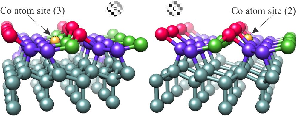
As a possible starting site for penetration into the 7-member ring, the energetically two most favorable quasi-stable Co atom sites on top of the Ge(111)21 surface are considered: Site (2) and site (3) (see Table 1). A 3D visualization of both configurations is presented in Fig. 9. The crystallographic directions of Fig. 9 are identical to those of Fig. 8 (a) (except for a rotation of the viewpoint angle with respect to the [111] direction). For the sites (2) and (3) the Co atoms are located in between two neighboring upper -bonded chain rows, at the center of the hexagonal 6-member Ge ring on the left [Fig. 9 (a)] and right hand side [Fig. 9 (b)] of the central upper -bonded chain row. A top view of these sites at the Ge(111)21 surface is presented in Fig. 10 (b). The Co atom at site (2) has one neighboring Ge down-atom and two neighboring Ge up-atoms, while the Co atom at site (3) has one neighboring Ge up-atom and two neighboring Ge down-atoms. One should note that for both sites the Co atom is already somewhat below the Ge layer, having a z-coordinate comparable to that of the down-atom for site (2) and lower than the down-atom for the site (3). As was the case for site (7), these Co atom sites do not destroy the reconstruction of the Ge(111)21 surface.
Next, both quasi-stable Co positions were taken as the starting positions for additional first principles DFT calculations with a 42 SC and using the same parameters as described above. The Co atom was forced to “move” into the bulk of the Ge by sequential decrements of its z-coordinate ( for each geometry relaxation step). After each forced sequential decrement of the z-coordinate, the position of the Co atom is kept fixed, while the Ge atoms are allowed to relax and the total energy is determined. By monitoring the total energy of the 42 SC during subsequent geometry relaxation steps, we are able to evaluate the potential barrier height that needs to be overcome by the Co atom when diffusing either from site (2) or from site (3) to site (7) without destroying the 21 surface reconstruction. First, when the Co atom is forced to move only very slightly below the Ge surface, the Co atom “bounces” back to its initial position. Second, upon a certain minimum translation along the z-direction (corresponding to a potential barrier ), the released Co atom continues to move further below the Ge surface to site (7) [see Figs. 10 (a) and (b)]. Both Co atom trajectories are visualized schematically in Fig. 10 (a).
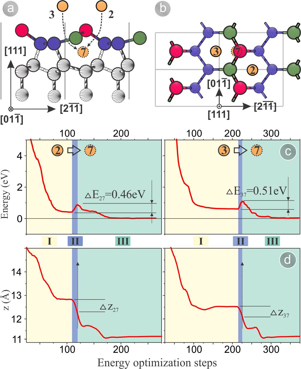
The variation of the total energy of the 42 SC (again with respect to of the 42 SC with the Co atom at site (7)) and the variation of the z-coordinate of the Co atom during the subsequent geometry relaxation steps are presented in Fig. 10 (c) and in Fig. 10 (d) for the two considered routes. Three regimes can be discerned. Regime I describes the energy gain and z-coordinate variations during movement of the Co atom from vacuum to either site (2) or site (3). Regime II corresponds to the “forced movement” of the Co atom into the bulk of the Ge up to the “point of no return” when the potential barrier has been overcome. Finally, regime III reflects the subsequent relaxation of the Co atom towards its final and stable position at site (7) in the 7-member Ge ring. The number of geometry relaxation steps for route (2)(7) and for route (3)(7) is 500 and 700, respectively. For clarity, geometry relaxation intervals where the total energy and the -value remain almost constant (at the end of the regimes I and III) are cut from Figs. 10 (c) and (d). The graphs presented in Fig. 10 (c) allow us to determine the potential barrier that the Co atom needs to overcome for route (2)(7) [(3)(7)]: [], corresponding to a change in z-coordinate [] in Fig. 10 (d).
To overcome the surface potential barrier for penetration below the Ge surface, a Co atom must have a sufficiently high (kinetic) energy upon deposition. In our experiments Co atoms are evaporated using an e-beam evaporator, where the Co material is heated to a high temperature around . Asano et al. (1992); Miller (1988) Atoms leaving an e-beam melt generally have a narrow energy distribution Chopra (1969) and the kinetic energy of the evaporated cloud of Co atoms, which is induced by the high temperature evaporation process can be roughly estimated using the equipartition theorem, yielding a mean atomic kinetic energy of about . Recently, however, Asano et al. have demonstrated experimentally that the velocity of evaporated atoms is typically even higher than the maximum velocity suggested by the ideal gas approximation. Asano et al. (1992) The increased velocity can be accounted for by a conversion of electron excitation energy to kinetic energy during the adiabatic expansion away from the heated material. If the gas flow of evaporated atoms cooled sufficiently during the adiabatic expansion, the resulting maximum velocity can be estimated as Uetake et al. (1991)
| (1) |
where is the specific heat ratio ( and are the specific heat at constant pressure and at constant volume per mole, respectively), is the gas constant and is the molar mass of the evaporated atom. is for an ideal mono-atomic gas. For , Eq. (1) yields a maximum velocity and hence the kinetic energy of the deposited Co atoms may exceed even a maximum value of . This kinetic energy allows a Co atom to overcome the surface energy barrier or that is encountered when penetrating below the Ge(111)21 surface following the route (2)(7) or the route (3)(7), respectively [see Fig. 10 (c)].
IV.5 DFT-based modeling of STM topography images
Our theoretical findings, related to the changes in surface energy and the potential barrier for penetration below the surface, support the idea of a noninvasive embedding of individual Co atoms in subsurface 7-member Ge rings. To verify the proposed “embedding model”, we investigated the electronic properties of the Co/Ge(111)21 system by simulating the corresponding STM topography images using DFT based calculations for a wide range of voltages, which allows for a direct and detailed comparison between theory and experiment. For this purpose we investigated the electronic structure of the Ge(111)21 surface for each of the possible Co atom locations described in Section IV.2, for both chain-left and chain-right isomers. The calculated quasi-stable geometries of the relaxed 84 SCs (9 and 8 possible geometries for the chain-left and chain-right isomer, respectively) were transferred to a larger 144 SC (size is ) for which we calculated the electronic properties in detail.
In order to construct STM constant current topography images based on the calculated electronic structure of the Co/Ge(111)21 system, the decay of the electron wave functions from the surface into the vacuum needs to be taken into account. Within the Tersoff-Hamann theory Tersoff and Hamann (1983, 1985) the dependence of the tunneling current on the applied tunneling voltage between an STM tip and a surface is given by
| (2) |
where is the Fermi function, is the tunneling matrix element between electronic states of the tip and electronic states of the surface, and () is the energy of the state () in the absence of tunneling. When we assume localized wave functions for the tip, will vary proportional to the amplitude of at the position , which corresponds to the center of the sphere that is used to approximate the tip apex. At low temperatures and for small tunneling voltages Eq. (2) reduces to
| (3) |
From Eq. (3) it follows that the tunneling current is proportional to the surface LDOS that is probed at position of the tip, integrated over an energy range from to . For constant tunneling current the STM tip essentially follows a contour of constant surface LDOS. However, because the surface wavefunctions decay exponentially into the vacuum region, numerical evaluation of for tip-surface distances of the order of several angstroms becomes a significant problem for DFT calculations. Paz et al. (2005) For this reason STM simulations are often restricted to (the vicinity of) the surface, which may yield incorrect results. To tackle this problem, we have used the 2D Fourier transform of the wavefunctions in combination with spatial extrapolation techniques Rohlfing et al. (2007) to evaluate the surface wave function in the vacuum region up to above the surface.
This way we calculated the STM topography images for all available Co atom sites and for both the chain-left and chain-right isomers (for a 144 SC) within an energy range between and and at distances up to above the surface. Perfect agreement between theory and experiment for the whole energy range can be achieved only for a Co atom located at site (7) for the chain-left isomer geometry. For site (7) we then calculated the electronic properties also for a 264 SC (size is , consisting of 1873 atoms) and a 235 SC (size is , consisting of 2071 atoms). CG geometry optimization for the chain-left(2) isomer with the Co atom located at site (7) within a 93 ( Å Å) SC was performed, similar to the calculations described in Section IV.2. We used the chain-left (1) and chain-left (2) isomers (see Section IV.1) for the 264 SC and 235 SC, respectively, to keep the Co atom in the center of the SC. Calculations for the 264 chain-left (1) SC and the 235 chain-left (2) SC yield identical results.
For our simulations of the STM topography images we have to rely on experimental spectra measured on the Ge(111)21 surface in order to take into account the dependence of the height z on the tunneling voltage in our calculations. The experimental dependence with an initial height addition of Shih et al. (1991) was used to determine the height above the Ge(111)21 surface at which simulated STM images are calculated. For low voltages, i.e. for energies close to , , while for high voltages above , .
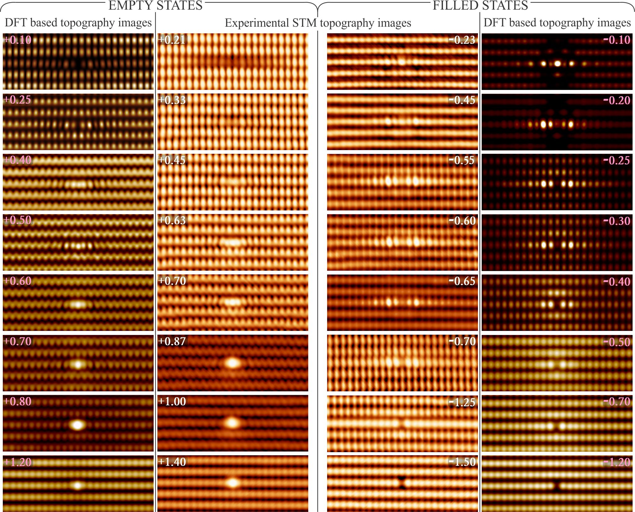
In Fig. 11 we present a series of experimental (inner columns) and calculated (outer columns) STM topography images for the filled (two right columns) and empty (two left columns) states regime within a wide range of tunneling voltages. Calculated STM topography images are obtained for a 235 SC with chain-left (2) isomer geometry with the Co atom at site (7). Experimental STM topography images are all recorded at the same location. The Co atom is well separated from other Co atoms, imlying there is no influence from neighboring Co atoms (see Section III).
As can be seen in Fig. 11, correspondence between the Co related features in the calculated and the experimental STM topography images is striking for the whole investigated voltage range. Concerning the precise tunneling voltage at which optimum correspondence is observed between theory and experiment there is a minor mismatch. This mismatch exhibits a non-linear dependence on the applied tunneling voltage for both the filled and empty states regime. At low tunneling voltages the difference in voltage is around for both the empty and filled states regime (see the first row of images in Fig. 11). For higher tunneling voltages, the difference increases to around and for the filled and empty states regime, respectively. Upon more careful comparison, it can be seen that the difference in voltage mainly affects the surrounding Ge(111)21 surface and not the Co atom itself. Indeed, maximum contrast related to the Co protrusion appears around in both the experimental [Fig. 11 and Fig. 6 (a4)] and the calculated STM topography images. Apart from the rather small difference in voltage, there is a very good agreement between the theoretically and experimentally observed electronic features for both the filled and empty states regime.
The results presented in Fig. 11 confirm that the calculated images of the Co/Ge(111) system exhibit all typical features that were observed in the voltage dependent STM investigation (Section III.3): (i) The Co induced strongly perturbed area comprises 2 SUCs on the upper -bonded chain row at moderate and high energies in the empty states regime; (ii) the perturbation has a mirror symmetry axis along the direction; (iii) the perturbation exhibits a clear asymmetry with respect to the direction; (iv) the Ge(111)21 surface exhibits a zigzag structure only at a specific tunneling voltage and this zigzag structure is perturbed near the Co atom.
In the filled states regime the calculated 1D Co induced perturbation along the -bonded chain row exhibits the highest contrast in the voltage range, whereas experimentally the highest contrast occurs around [see Fig. 6 (b3) and Fig. 11]. At these energies the Co induced perturbed atomic corrugation along the upper -bonded chain row in the calculated and experimental STM topography image match very well. At energies below the Co atom appears as an atomic size vacancy in the upper -bonded chain row for both the calculated and experimental STM topography.
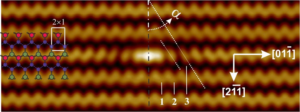
In the calculated images the zigzag structure of the Co containing upper -bonded chain rows is observed at empty state energy around (see Fig. 12). On the other hand, this zigzag structure appears around in the experimental STM images (see Section III.2). The determination of the angle in Fig. 12 allows for an easy comparison to Fig. 4 (d). It can be seen that, apart from a small energy mismatch, the Co induced perturbation of the calculated zigzag structure again perfectly matches the experimental observation.
The energy mismatch between the calculated and experimental STM results can be related to the doping of the investigated Ge crystals (p-type Ge crystals with a low dopant concentration are used in this work), which is not included in the DFT modeling. Since the surface and bulk bands shift in energy depending on the type of doping and on the doping level, it can be expected that the Co induced perturbations shift in energy as well. On the other hand, whereas deposition of ML of Co did not lead to changes of the Ge(111)21 electronic structures in the experiments, the incorporation of the Co atom in the DFT model may induce a “doping” effect of the Co/Ge(111)21 system due to the finite size of the SC. For the 235 SC, the Co/Ge ratio is 1/2071, which corresponds to a heavily doped Ge crystal. As already mentioned in Section III.2, the precise value of the tunneling voltage is found to depend on the semiconductor type and on the doping concentration. E.g., heavily doped n-Ge(111)21 surfaces (phosphor doping level , surface preparation as described in Section II) are found to have , which is in good agreement with the calculated tunneling voltage of .
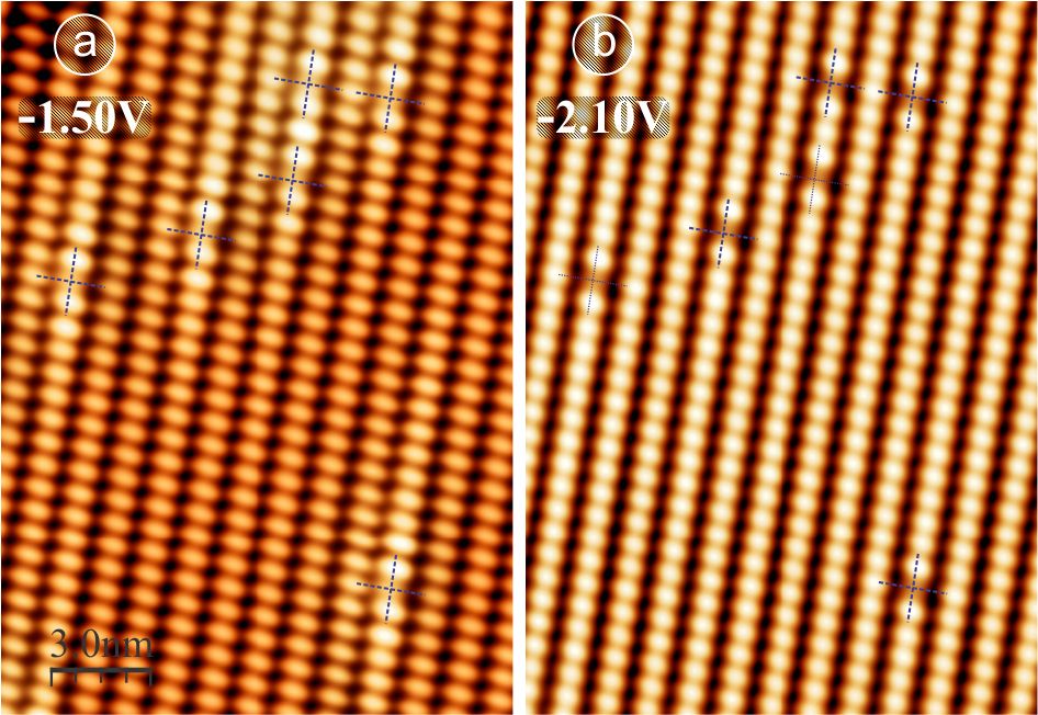
Finally, we investigated the influence of the doping level on the appearance of the clean Ge(111)21 surface and the Co/Ge(111)21 system in experimental STM topography images. As indicated above, it can be expected that the Co induced perturbations shift in energy, since the surface and bulk bands shift in energy depending on the type of doping and the doping level. In Fig. 13 we present two experimental filled states STM topography images of a low doped n-type Ge(111)21 surface. The Ge crystal was doped by P at a doping level to (). Surface preparation and Co deposition are performed as described in Section II. At low temperatures (), these samples exhibit a detectable tunneling current in the filled states regime only at tunneling voltages below . Interestingly, the above described Co induced perturbations appear at significantly different energies for this low doped sample. The features observed in Fig. 13 (a) for the n-type Ge(111)21 surface are observed around for the p-type Ge(111)21 surface (see Fig. 11), corresponding to an energy shift of about . A similar energy shift can be inferred by comparison of Fig. 13 (b) and Fig. 11. The energy shifts between the STM experiments and the DFT calculations in Fig. 11 may therefore be attributed to doping effects. Alternatively, the observed energy shifts may also be related to the intrinsic deficiency of LDA with respect to the quantitative determination of band gap values of semiconductor materials.
IV.6 Co/Ge(111)21 electronic properties and Co–Ge bonding characteristics
| Co neighboring atoms | Co–Ge distance | ||
|---|---|---|---|
| Co–Ge(1) | 2.687 | ||
| Co–Ge(2) | 2.404 | ||
| Co–Ge(3) | 2.404 | ||
| Co–Ge(4) | 2.415 | ||
| Co–Ge(5) | 2.243 |
| A. Co/Ge(111)21 | |||||
|---|---|---|---|---|---|
| Bond (atom–atom) | Ge(1) | Ge(2) | Ge(3) | Ge(4) | Ge(5) |
| Ge–Ge | 0.368 | 0.444 | 0.396 | 0.368 | 0.228 |
| Ge–Ge | 0.394 | 0.394 | 0.445 | 0.401 | 0.356 |
| Ge–Ge | 0.396 | 0.409 | 0.408 | 0.228 | 0.401 |
| Ge–Ge | 0.067 | 0.065 | 0.401 | 0.353 | |
| Co–Ge | 0.120 | 0.241 | 0.239 | 0.224 | 0.231 |
| Electron pop. | 4.205 | 3.891 | 3.889 | 3.943 | 3.884 |
| B. Ideal (21) | |||||
| Bond (atom–atom) | Ge(1′) | Ge(2′) | Ge(3′) | Ge(4′) | Ge(5′) |
| Ge–Ge | 0.412 | 0.475 | 0.475 | 0.412 | 0.395 |
| Ge–Ge | 0.476 | 0.476 | 0.456 | 0.402 | 0.406 |
| Ge–Ge | 0.475 | 0.435 | 0.435 | 0.395 | 0.405 |
| Ge–Ge | - | 0.089 | 0.089 | 0.402 | 0.406 |
| Electron pop. | 4.172 | 3.882 | 3.859 | 3.982 | 3.961 |
In this section we discuss the chemical bonds that are formed between the Co atom at site (7) and its surrounding Ge atoms [labeled in Fig. 15 (b1)] underneath the Ge(111)21 surface. The amount of possible chemical bonds can be roughly estimated by relying on a simple analysis of the Co-Ge bond lengths. For a single bond between a Co and a Ge atom the bond length can be estimated as the sum of the Co and Ge covalent radii, which is Å. The calculated distances between the Co atom and the neighboring Ge atoms for the 84 SC equilibrium geometry (see subsection IV.2) are listed in Table 2. Among the listed Ge atoms, Ge atoms (2) to (5) are most likely to form a covalent bond with the Co atom. The distances between the Co atom and these Ge atoms are, however, slightly larger (1-2%) than , which can be attributed to the employed LDA (an overestimation of the bond lengths by a few percent is typical for LDA). On the other hand, the calculated Co–Ge(1) distance is significantly larger (around 13%) than , implying that the formation of a bond between the Co atom and the Ge(1) up-atom can be excluded.
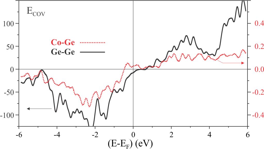
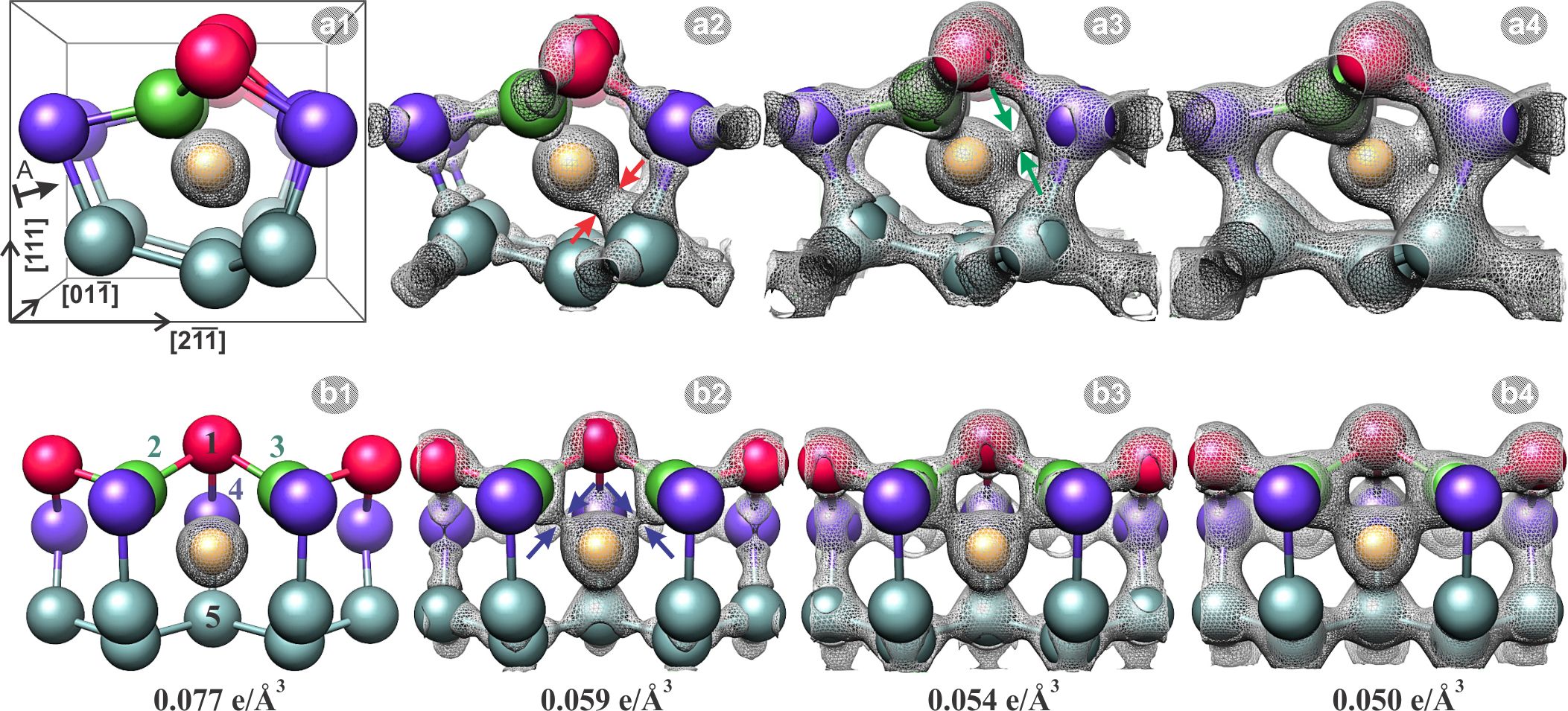
An estimate of the atomic charges, electron transfer and covalent interactions between the Co atom at site (7) and the neighboring Ge atoms [labeled in Fig. 15 (b1), also see Table 2] can be obtained more qualitatively from the calculated number of electrons inside the atomic spheres and from the Mulliken populations. Mulliken (1955) The Mulliken electron orbital overlap populations (calculated for the 235 SC) of Ge atoms (1) to (5) both with (perturbed -bonded chain row of the Co/Ge(111)21 system) and without (unperturbed -bonded chain row of the Ge(111)21 surface) the Co atom are given in Table 3 (A) and in Table 3(B), respectively. The (unperturbed) bulk atoms Ge(4′) and Ge(5′) have four Ge–Ge covalent bonds, with an electron orbital overlap population around ( hybridization). On the other hand, up-atom Ge(1′) and down-atoms Ge(2′,3′) have only three covalent bonds ( hybridization): A fourth bond is absent or at least strongly reduced (Mulliken overlap populations are less than 22% of the Ge–Ge bulk covalent bond). Co-induced changes in the Mulliken overlap population of the neighboring Ge atoms and the atom population can be traced by comparison of Table 3 (A) to Table 3 (B). The calculations reveal that no significant charge redistribution between the Co atom and the surface and bulk Ge atoms occurs, i.e. the electron population of the Co atom remains close to that of a neutral Co atom (). The Co atom exhibits four covalent bonds with Mulliken overlap populations that are 56% to 60% of the Ge–Ge bulk covalent bond. There exists a weak interaction with the Ge(1) up-atom as well (see Table 3 (A)). Because of the very low overlap population (30% of Ge–Ge bulk bond) and the very weak charge transfer between Co and Ge(1), however, the interaction between the Co and Ge(1) up-atom should not be considered as a fifth covalent bond.
The energy of the covalent Co-Ge bonds can be estimated as the total energy difference between a Co atom that is “bonded” [Co atom located at site (7)] or “not bonded” to the Ge lattice. Calculations for the “not bonded” case were performed for a 42 SC with the Co atom placed 4Å above the Ge surface. The total energy difference is found to be . Considering four Co–Ge bonds as discussed above, the (average) energy of a single Co–Ge bond is hence , which is significantly lower than the energy of the covalent Ge–Ge bond ().
The analysis of the bond lengths and the Mulliken overlap populations are indicative of rather weak Co–Ge bonds, which can also be concluded from our experimental observation that Co atoms diffuse even at lower temperatures. Muzychenko et al. (2011) More precisely, in spite of the low sample temperature () during Co deposition, the majority (around 87%) of the Co atoms diffuses along -bonded chain rows to surface/subsurface defects (including DBs, MASs, and subsurface Ga impurities), which can be related to the weak Co–Ge bonds. The remaining 13% can be retrieved as individual (subsurface) Co atoms at the cold Ge surface and they diffuse as well to surface/subsurface defects after warming the substrate up to room temperature. For a more detailed discussion we refer the reader to Ref. [Muzychenko et al. (2011)].
The chemical bonding mechanism between the Co and Ge atoms involved in the DFT electronic structure calculations can be investigated in more detail by evaluating the crystal orbital overlap population/Hamiltonian population (COOP/COHP). Hoffmann (1993); Dronskowski and Bloechl (1993) We have used an alternative COOP/COHP based approach that allows to calculate the relevant physical quantities independent of the choice of zero of the potential by relying on the so-called “covalent bond energy” (). Bester and Fähnle (2001) COOP and calculations are known to yield similar results, while the COOP method generally overestimates the magnitude of the anti-bonding states when defined within a plane-wave basis set. Paul-Boncour and Matar (2004) Figure 14 presents our calculation for the Co–Ge and Ge–Ge bulk interactions in an energy range of around the Fermi level. Note that the values (y-ordinate) are plotted without any units and can only be interpreted qualitatively. Negative, positive, and zero values of correspond to bonding, anti-bonding, and non-bonding interactions, respectively. The spectra confirm the stability of the Co/Ge system. Strong bonding interactions exist for Ge–Ge from the bottom of the VB up to the Fermi level, while for the Co–Ge a strong bonding interaction is found only up to around . Between and the Fermi level, Co–Ge anti-bonding interactions occur, which may explain the experimentally observed thermal instability of the Co/Ge system (the covalent Co–Ge bonds are weaker than the Ge–Ge bulk bonds).
Finally, we calculated charge electron density maps to visualize the Co–Ge bonds. In Fig. 15 we present isosurface maps of the spatial electron charge density for isosurface values ranging from Å3 down to Å3. High electron densities related to the Ge–Ge covalent bonds gradually appear above Å3 in Figs. 15 (a2,b2) to (a4,b4). Moreover, zones of high electron localization between the Co atom and the surrounding Ge atoms can be observed. A zone of high electron localization exists between the Co atom and the Ge(5) atom in Fig. 15 (a2) (indicated by red arrows). Two additional symmetrical zones of high electron localization can be observed between the Co atom and the Ge(2) and Ge(3) down-atoms in Fig. 15 (b2) (indicated by the blue arrows). A fourth Co–Ge bond can be related to the high electron localization zone between the Co atom and the Ge(4) atom in Fig. 15 (a3) (indicated by the green arrows). As could be expected from our above analysis, there occurs no high electron localization zone between the Co atom and the up-atom Ge(1), which additionally confirms that both atoms are not bonded. The findings related to the bond lengths, the Mulliken overlap populations and the calculations are hence in agreement with the isosurface charge density maps. We therefore conclude that the Co atom forms a bond with four neighboring Ge atoms, corresponding to a Co4+ valence state and a 3 electron configuration. It is known that Co has a wide range of valence states due to its various spin configurations, implying Co 3 ions can exist in several spin configurations. Sen and Bartolotti (1992); Ravindran et al. (1999) An extension of our DFT model for the embedding of a Co atom in the Ge lattice by including spin-dependent calculations will be a topic of future research.
V Conclusion
Noninvasive embedding of individual Co atoms into clean Ge(111)21 surfaces was systematically investigated by means of STM experiments and DFT calculations. STM experiments indicate that these Co atoms appear exclusively at upper -bonded chain rows after deposition on cold Ge(111)21 surfaces (). Analysis of the voltage dependent STM images reveals that all adsorbed Co atoms induce an identical anisotropic electronic perturbation of the surrounding Ge surface and clear 1D confinement along -bonded chains. Relying on DFT based calculations we demonstrated that the energetically most favorable position of a Co atom is attained by penetration into the Ge(111)21 surface. The Co atom occupies a quasi-stationary position within the big 7-member Ge ring of the Ge(111)21 reconstruction in between the and atomic layer beneath the surface. The embedded Co atom induces an electronic asymmetry of the -bonded chain with respect to the direction, which allows us to determine that the Ge(111)21 surface reconstruction of all investigated Ge samples consists of domains with chain-left geometry exclusively. Calculated STM images based on our DFT approach match very well the experimental STM images of the Co/Ge(111)21 system within the investigated range of tunneling voltages. Finally, DFT based calculations of the Co–Ge bond strength reveal the formation of four covalent bonds, corresponding to a Co4+ valence state and a 3 electron configuration. Our findings open interesting perspectives for investigations of subsurface 1D (nanowires) and 2D (islands) nanostructures that are expected to form at a higher coverage of Co on Ge(111).
Acknowledgements.
The research in Moscow has been supported by the Russian Foundation for Basic Research (RFBR) grants and by the computing facilities of the M.V. Lomonosov Moscow State University (MSU) Research Computing Center. The research in Leuven has been supported by the Research Foundation - Flanders (FWO, Belgium) as well as by the Belgian Interuniversity Attraction Poles (IAP) and the Flemish Concerted Action (GOA) research programs. K. S. is a postdoctoral researcher of the FWO.References
- Bhattacharya et al. (2004) P. Bhattacharya, S. Ghosh, and A. Stiff-Roberts, Annual Rev. of Mat. Res. 34, 1 (2004).
- Kuo et al. (2005) Y.-H. Kuo, Y. K. Lee, Y. Ge, S. Ren, J. E. Roth, T. I. Kamins, D. A. B. Miller, and J. S. Harris, Nature 437, 1334 (2005).
- Whalley et al. (2007) A. C. Whalley, M. L. Steigerwald, X. Guo, and C. Nuckolls, J. Am. Chem. Soc. 129, 12590 (2007).
- Grigoriev et al. (2006) A. Grigoriev, J. Sköldberg, G. Wendin, and Z. Crljen, Phys. Rev. B 74, 045401 (2006).
- Parks et al. (2010) J. J. Parks, A. R. Champagne, T. A. Costi, W. W. Shum, A. N. Pasupathy, E. Neuscamman, S. Flores-Torres, P. S. Cornaglia, A. A. Aligia, C. A. Balseiro, et al., Science 328, 1370 (2010).
- Prinz (1995) G. A. Prinz, Physics Today 48, 58 (1995).
- Haider et al. (2009) M. B. Haider, J. L. Pitters, G. A. DiLabio, L. Livadaru, J. Y. Mutus, and R. A. Wolkow, Phys. Rev. Lett. 102, 046805 (2009).
- Tan et al. (2009) K. Y. Tan, K. W. Chan, M. Mttnen, A. Morello, C. Yang, J. van Donkelaar, A. Alves, J.-M. Pirkkalainen, D. N. Jamieson, R. G. Clark, et al., Nano Lett. 10, 11 (2009).
- Bracht et al. (2009) H. Bracht, S. Schneider, J. N. Klug, C. Y. Liao, J. L. Hansen, E. E. Haller, A. N. Larsen, D. Bougeard, M. Posselt, and C. Wündisch, Phys. Rev. Lett. 103, 255501 (2009).
- Wundisch et al. (2009) C. Wundisch, M. Posselt, B. Schmidt, V. Heera, T. Schumann, A. Mucklich, R. Grotzschel, W. Skorupa, T. Clarysse, E. Simoen, et al., Appl. Phys. Lett. 95, 252107 (pages 3) (2009).
- Sze and Irvin (1968) S. M. Sze and J. C. Irvin, Solid-State Electronics 11, 599 (1968).
- Lee et al. (2005) M. L. Lee, E. A. Fitzgerald, M. T. Bulsara, M. T. Currie, and A. Lochtefeld, J. Appl. Phys. 97, 011101 (pages 28) (2005).
- Leitz et al. (2002) C. W. Leitz, M. T. Currie, M. L. Lee, Z.-Y. Cheng, D. A. Antoniadis, and E. A. Fitzgerald, J. Appl. Phys. 92, 3745 (2002).
- Claeys and Simoen (2007) C. Claeys and E. Simoen, Germanium-Based Technologies-From Materials to Devices (Elsevier, Amsterdam, 2007).
- Appenzeller et al. (2004) J. Appenzeller, Y.-M. Lin, J. Knoch, and P. Avouris, Phys. Rev. Lett. 93, 196805 (2004).
- Chui et al. (2003) C. O. Chui, K. Gopalakrishnan, P. B. Griffin, J. D. Plummer, and K. C. Saraswat, Appl. Phys. Lett. 83, 3275 (2003).
- Reimann and Manninen (2002) S. M. Reimann and M. Manninen, Rev. Mod. Phys. 74, 1283 (2002).
- Nilius et al. (2002) N. Nilius, T. M. Wallis, and W. Ho, Science 297, 1853 (2002).
- Wang et al. (2004) J. Wang, M. Li, and E. I. Altman, Phys. Rev. B 70, 233312 (2004).
- Schouteden et al. (2009) K. Schouteden, E. Lijnen, D. A. Muzychenko, A. Ceulemans, L. F. Chibotaru, P. Lievens, and C. V. Haesendonck, Nanotechnology 20, 395401 (2009).
- Kouwenhoven et al. (2001) L. P. Kouwenhoven, D. G. Austing, and S. Tarucha, Rep. Prog. Phys. 64, 701 (2001).
- Wolf et al. (2001) S. A. Wolf, D. D. Awschalom, R. A. Buhrman, J. M. Daughton, S. von Moln r, M. L. Roukes, A. Y. Chtchelkanova, and D. M. Treger, Science 294, 1488 (2001).
- Žutić et al. (2004) I. Žutić, J. Fabian, and S. Das Sarma, Rev. Mod. Phys. 76, 323 (2004).
- Zeng et al. (2004) C. Zeng, W. Zhu, S. C. Erwin, Z. Zhang, and H. H. Weitering, Phys. Rev. B 70, 205340 (2004).
- Profeta et al. (2004) G. Profeta, S. Picozzi, A. Continenza, and C. Franchini, Phys. Rev. B 70, 155307 (2004).
- Oncel et al. (2005) N. Oncel, A. van Houselt, J. Huijben, A.-S. Hallbäck, O. Gurlu, H. J. W. Zandvliet, and B. Poelsema, Phys. Rev. Lett. 95, 116801 (2005).
- Schäfer et al. (2006) J. Schäfer, D. Schrupp, M. Preisinger, and R. Claessen, Phys. Rev. B 74, 041404 (2006).
- Stekolnikov et al. (2008a) A. A. Stekolnikov, F. Bechstedt, M. Wisniewski, J. Schäfer, and R. Claessen, Phys. Rev. Lett. 100, 196101 (2008a).
- Stekolnikov et al. (2008b) A. A. Stekolnikov, J. Furthmüller, and F. Bechstedt, Phys. Rev. B 78, 155434 (2008b).
- Vanpoucke and Brocks (2010) D. E. P. Vanpoucke and G. Brocks, Phys. Rev. B 81, 085410 (2010).
- Sauer et al. (2010) S. Sauer, F. Fuchs, F. Bechstedt, C. Blumenstein, and J. Schäfer, Phys. Rev. B 81, 075412 (2010).
- van Houselt et al. (2008) A. van Houselt, M. Fischer, B. Poelsema, and H. J. W. Zandvliet, Phys. Rev. B 78, 233410 (2008).
- Tomatsu et al. (1007) K. Tomatsu, K. Nakatsuji, T. Iimori, and F. Komori, Surf. Sci. 601, 1736 (1007).
- Fischer et al. (2007) M. Fischer, A. van Houselt, D. Kockmann, B. Poelsema, and H. J. W. Zandvliet, Phys. Rev. B 76, 245429 (2007).
- Wang et al. (2006) J. Wang, M. Li, and E. I. Altman, J. Appl. Phys. 100, 113501 (pages 7) (2006).
- Lince et al. (1983) J. R. Lince, J. G. Nelson, and R. S. Williams, J. Vac. Sci. Tech. B 1, 553 (1983).
- Chan and Altman (2002) L. H. Chan and E. I. Altman, Phys. Rev. B 66, 155339 (2002).
- Parkin (1993) S. S. P. Parkin, Phys. Rev. Lett. 71, 1641 (1993).
- Tsay et al. (2002) J. S. Tsay, Y. D. Yao, K. C. Wang, W. C. Cheng, and C. S. Yang, Surf. Sci. 507-510, 498 (2002).
- Ryan et al. (2004) P. Ryan, R. P. Winarski, D. J. Keavney, J. W. Freeland, R. A. Rosenberg, S. Park, and C. M. Falco, Phys. Rev. B 69, 054416 (2004).
- Tsay et al. (2004a) J. S. Tsay, H. Y. Nieh, Y. D. Yao, Y. T. Chen, and W. C. Cheng, Surf. Sci. 566-568, 226 (2004a).
- Tsay et al. (2005) J. S. Tsay, C. W. Su, C. H. Hwang, and Y. D. Yao, J. Vac. Sci. Tech. A 23, 781 (2005).
- Chang et al. (2006) H. W. Chang, J. S. Tsay, Y. L. Chiou, K. T. Huang, W. Y. Chan, and Y. D. Yao, J. Appl. Phys. 99, 08J705 (pages 3) (2006).
- Tsay et al. (2003) J. S. Tsay, H. Y. Nieh, C. S. Yang, Y. D. Yao, and T. S. Chin, J. Appl. Phys. 93, 8728 (2003).
- Tsay et al. (2004b) J. Tsay, H. Nieh, Y. Yao, and T. Chin, J. Magn. Magn. Mat. 282, 78 (2004b).
- Su et al. (2006) C. Su, J. Tsay, and Y. Yao, J. Magn. Magn. Mat. 304, e41 (2006).
- Barth et al. (1990) J. V. Barth, H. Brune, G. Ertl, and R. J. Behm, Phys. Rev. B 42, 9307 (1990).
- Schouteden et al. (2008) K. Schouteden, E. Lijnen, E. Janssens, A. Ceulemans, L. F. Chibotaru, P. Lievens, and C. V. Haesendonck, New J. Phys. 10, 043016 (2008).
- Horcas et al. (2007) I. Horcas, R. Fernandez, J. M. Gomez-Rodriguez, J. Colchero, J. Gomez-Herrero, and A. M. Baro, Rev. Sci. Inst. 78, 013705 (2007).
- Northrup and Cohen (1983) J. E. Northrup and M. L. Cohen, Phys. Rev. B 27, 6553 (1983).
- Pandey (1981) K. C. Pandey, Phys. Rev. Lett. 47, 1913 (1981).
- Feenstra and Slavin (1991) R. M. Feenstra and A. J. Slavin, Surf. Sci. 251-252, 401 (1991).
- Feenstra et al. (2001) R. M. Feenstra, G. Meyer, F. Moresco, and K. H. Rieder, Phys. Rev. B 64, 081306 (2001).
- Einaga et al. (1998) Y. Einaga, H. Hirayama, and K. Takayanagi, Phys. Rev. B 57, 15567 (1998).
- Muzychenko et al. (2010) D. A. Muzychenko, S. V. Savinov, V. N. Mantsevich, N. S. Maslova, V. I. Panov, K. Schouteden, and C. Van Haesendonck, Phys. Rev. B 81, 035313 (2010).
- Guo et al. (2004) H. M. Guo, H. W. Liu, Y. L. Wang, H. J. Gao, H. X. Shang, Z. W. Liu, H. M. Xie, and F. L. Dai, Nanotech. 15, 991 (2004).
- Bechstedt et al. (2001) F. Bechstedt, A. A. Stekolnikov, J. Furthmüller, and P. Käckell, Phys. Rev. Lett. 87, 016103 (2001).
- Kobayashi (2003) K. Kobayashi, Phys. Rev. B 68, 075308 (2003).
- Nicholls et al. (1983) J. M. Nicholls, G. V. Hansson, R. I. G. Uhrberg, and S. A. Flodström, Phys. Rev. B 27, 2594 (1983).
- Nicholls et al. (1984) J. M. Nicholls, G. V. Hansson, U. O. Karlsson, R. I. G. Uhrberg, R. Engelhardt, K. Seki, S. A. Flodström, and E. E. Koch, Phys. Rev. Lett. 52, 1555 (1984).
- Nicholls et al. (1985) J. M. Nicholls, P. Maartensson, and G. V. Hansson, Phys. Rev. Lett. 54, 2363 (1985).
- Muzychenko et al. (2011) D. A. Muzychenko, K. Schouteden, V. I. Panov, and C. Van Haesendonck, Submitted to Nanotechnology (available online: http://arxiv.org/abs/1201.0735) (2011).
- Nie et al. (2004) S. Nie, R. M. Feenstra, J. Y. Lee, and M.-H. Kang, J. Vac. Sci. Tech. A 22, 1671 (2004).
- Trappmann et al. (1999) T. Trappmann, C. Surgers, and H. v. Lohneysen, Appl. Phys. A 68, 167 (1999), URL http://dx.doi.org/10.1007/s003390050872.
- Garleff et al. (2005) J. K. Garleff, M. Wenderoth, R. G. Ulbrich, C. Sürgers, and H. v. Löhneysen, Phys. Rev. B 72, 073406 (2005).
- Garleff et al. (2007) J. K. Garleff, M. Wenderoth, R. G. Ulbrich, C. Sürgers, H. v. Löhneysen, and M. Rohlfing, Phys. Rev. B 76, 125322 (2007).
- Himpsel et al. (1984) F. J. Himpsel, P. M. Marcus, R. Tromp, I. P. Batra, M. R. Cook, F. Jona, and H. Liu, Phys. Rev. B 30, 2257 (1984).
- Tromp et al. (1984) R. M. Tromp, L. Smit, and J. F. van der Veen, Phys. Rev. B 30, 6235 (1984).
- Alerhand et al. (1985) O. L. Alerhand, D. C. Allan, and E. J. Mele, Phys. Rev. Lett. 55, 2700 (1985).
- Northrup et al. (1991) J. E. Northrup, M. S. Hybertsen, and S. G. Louie, Phys. Rev. Lett. 66, 500 (1991).
- Takeuchi et al. (1991) N. Takeuchi, A. Selloni, A. I. Shkrebtii, and E. Tosatti, Phys. Rev. B 44, 13611 (1991).
- Rohlfing et al. (2000) M. Rohlfing, M. Palummo, G. Onida, and R. Del Sole, Phys. Rev. Lett. 85, 5440 (2000).
- Hirayama et al. (2000) H. Hirayama, N. Sugihara, and K. Takayanagi, Phys. Rev. B 62, 6900 (2000).
- Kohn and Sham (1965) W. Kohn and L. J. Sham, Phys. Rev. 140, A1133 (1965).
- Perdew and Zunger (1981) J. P. Perdew and A. Zunger, Phys. Rev. B 23, 5048 (1981).
- Ordejón et al. (1996) P. Ordejón, E. Artacho, and J. M. Soler, Phys. Rev. B 53, R10441 (1996).
- Sánchez-Portal et al. (1997) D. Sánchez-Portal, P. Ordejón, E. Artacho, and J. M. Soler, Int. J. Quant. Chem. 65, 453 (1997).
- Soler et al. (2002) J. M. Soler, E. Artacho, J. D. Gale, A. García, J. Junquera, P. Ordejón, and D. Sánchez-Portal, J. Phys.: Cond. Matt. 14, 2745 (2002), URL http://stacks.iop.org/0953-8984/14/i=11/a=302.
- Troullier and Martins (1991) N. Troullier and J. L. Martins, Phys. Rev. B 43, 1993 (1991).
- Uberuaga et al. (2000) B. P. Uberuaga, M. Leskovar, A. P. Smith, H. Jónsson, and M. Olmstead, Phys. Rev. Lett. 84, 2441 (2000).
- Lin et al. (1992) D.-S. Lin, T. Miller, and T.-C. Chiang, Phys. Rev. B 45, 11415 (1992).
- Gurlu et al. (2004) O. Gurlu, H. J. W. Zandvliet, B. Poelsema, S. Dag, and S. Ciraci, Phys. Rev. B 70, 085312 (2004).
- Smith et al. (1989) G. A. Smith, L. Luo, S. Hashimoto, W. M. Gibson, and N. Lewis, J. Vac. Sci. Tech. A 7, 1475 (1989).
- Asano et al. (1992) T. Asano, N. Uetake, and K. Suzuki, J. Nucl. Sci.Tech. 29, 1194 (1992).
- Miller (1988) P. R. Miller, Atomic and Molecular Beam Methods (Oxford University Press, Oxford, 1988).
- Chopra (1969) K. L. Chopra, Thin Film Phenomenona (McGraw-Hill, New York, 1969).
- Uetake et al. (1991) N. Uetake, T. Asano, and K. Suzuki, Rev. Sci. Inst. 62, 1942 (1991).
- Tersoff and Hamann (1983) J. Tersoff and D. R. Hamann, Phys. Rev. Lett. 50, 1998 (1983).
- Tersoff and Hamann (1985) J. Tersoff and D. R. Hamann, Phys. Rev. B 31, 805 (1985).
- Paz et al. (2005) O. Paz, I. Brihuega, J. M. Gómez-Rodríguez, and J. M. Soler, Phys. Rev. Lett. 94, 056103 (2005).
- Rohlfing et al. (2007) M. Rohlfing, R. Temirov, and F. S. Tautz, Phys. Rev. B 76, 115421 (2007).
- Shih et al. (1991) C. K. Shih, R. M. Feenstra, and G. V. Chandrashekhar, Phys. Rev. B 43, 7913 (1991).
- Mulliken (1955) R. S. Mulliken, J. Chem. Phys. 23, 1833 (1955).
- Hoffmann (1993) R. Hoffmann, J. Phys.: Cond. Matter 5, A1 (1993).
- Dronskowski and Bloechl (1993) R. Dronskowski and P. E. Bloechl, J. Phys. Chem. 97, 8617 (1993).
- Bester and Fähnle (2001) G. Bester and M. Fähnle, J. Phys.: Cond. Matt. 13, 11541 (2001), URL http://stacks.iop.org/0953-8984/13/i=50/a=313.
- Paul-Boncour and Matar (2004) V. Paul-Boncour and S. F. Matar, Phys. Rev. B 70, 184435 (2004).
- Sen and Bartolotti (1992) K. D. Sen and L. J. Bartolotti, Phys. Rev. A 45, 2076 (1992).
- Ravindran et al. (1999) P. Ravindran, P. A. Korzhavyi, H. Fjellvåg, and A. Kjekshus, Phys. Rev. B 60, 16423 (1999).