An accurate measurement of electron beam induced displacement cross sections for single-layer graphene
Abstract
We present an accurate measurement and a quantitative analysis of electron-beam induced displacements of carbon atoms in single-layer graphene. We directly measure the atomic displacement (“knock-on”) cross section by counting the lost atoms as a function of the electron beam energy and applied dose. Further, we separate knock-on damage (originating from the collision of the beam electrons with the nucleus of the target atom) from other radiation damage mechanisms (e.g. ionization damage or chemical etching) by the comparison of ordinary () and heavy () graphene. Our analysis shows that a static lattice approximation is not sufficient to describe knock-on damage in this material, while a very good agreement between calculated and experimental cross sections is obtained if lattice vibrations are taken into account.
Radiation damage is one of the key limitations of high-resolution transmission electron microscopy (HR-TEM) Egerton2004 . In particular, the continuous improvements in instrumental resolution Haider1998 ; Batson2002 inevitably entail increased doses per area that need to be applied to a sample. The need for high doses is further increased for new techniques such as single-atom or single-atomic-column spectroscopy Batson1993 ; Kaiser2002 ; Muller2008 ; Suenaga2009 , atomic resolution electron tomography BarSadan2008 , or the analysis of charge distributions from very high signal-to-noise ratio HR-TEM images Meyer2011 . For light element materials, such as carbon nanotubes Iijima1991 ; Iijima1993 , fullerenes Kroto1985 , graphene Novoselov2004 ; Geim2007 , boron nitride Pacile2008 ; Novoselov2005 , and probably many more, the dose limitation is particularly severe for three reasons: First, it is obvious, that knock-on damage cross sections will be higher for low atomic number elements Banhart1999 . Second, the light elements produce less contrast than heavier elements, so that even higher doses are needed to obtain a sufficient signal to noise ratio. And third, most of the novel materials from light elements, such as graphene or carbon nanotubes, appear in the form of low dimensional allotropes that have only one or a few atoms in a typical projection of a high-resolution image. While almost all atomic spacings can in principle be resolved by the currently available instrumentation, the question remains whether a sample is stable under the beam until an image has been acquired. In spite of a wide range of previous studies concerning irradiation damage in carbon nanostructures LUCAS1964 ; Crespi1996a ; Banhart1999 ; Smith2001 ; Krasheninnikov2005 ; Zobelli2007a ; Molhave2007 ; Warner2009a , a quantitative experimental determination of atomic displacement cross sections for this important class of materials is absent. In fact, only very few quantitative measurements of electron-beam induced displacement cross sections CHERNS1976 ; Egerton2010 (beyond damage threshold measurements Egerton1977 ; Zag1983 ) can be found in the literature. The understanding of irradiation effects is also important for targeted irradiation-induced modifications of a material: For the case of graphene, for example, a controlled introduction of vacancies and non-hexagonal rings may lead to derived hybridized carbon sheets with specific properties Crespi1996 ; Terrones2000 ; Lusk2008 ; Fischbein2008 ; Kotakoski2011 ; Krasheninnikov2007 .
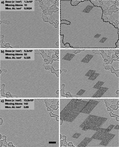
Here, we present an extensive measurement and analysis of electron-beam induced displacements. We directly count the number of ejected atoms under irradiation as functions of dose, dose rate, and electron energy. Suspended single layer graphene sheets provide the perfect test sample for this analysis: They can be prepared in a precisely defined geometry (1 atomic layer thick, hexagonal lattice, with practically no defects initially), are relatively easy to model, and the number of ejected atoms in multi-vacancy configurations can be directly obtained from HRTEM images Meyer2008a ; Kotakoski2011 . Under 80 keV electron irradiation, the defect free graphene lattice remains undisturbed up to very high doses Meyer2008a ; Meyer2011 but knock-on damage begins already a few keV above this energy LUCAS1964 ; Crespi1996a ; Banhart1999 ; Smith2001 ; Krasheninnikov2005 ; Zobelli2007a ; Molhave2007 ; Warner2009a . Importantly, for energies near the knock-on threshold, the changes in the lattice occur slowly, so that the appearance and growth of multi-vacancies can be directly observed in real time. In this way, we can count the number of lost atoms as a function of applied dose and for different acceleration voltages, hence providing a direct measurement of the knock-on cross section.
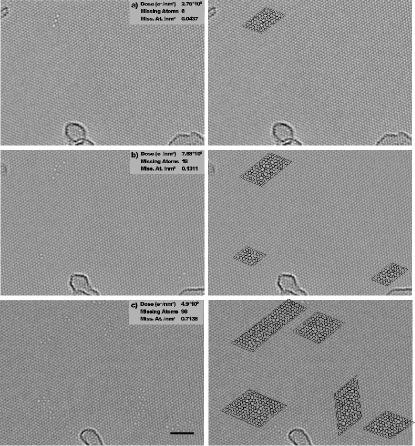
We present insights from a tremendous data set that was obtained for the purpose of quantitating the radiation damage in graphene: We have obtained and analyzed image sequences as shown in Fig. 1 for many acceleration voltages (80, 90, 95, 100 kV), and for both, the “normal” graphene sample and isotope-enriched “heavy graphene” samples. For all of this data, the defect configurations were analyzed at different doses of exposure, and the number of missing atoms was counted (see supplementary information for further examples from the data set). We also studied graphene under 20 keV electron irradiation Kaiser2011a , in order to obtain a further distinction between knock-on damage and other effects such as chemical etching or radiolysis.
Experimentally, we prepared graphene membranes by mechanical exfoliation and transfer to TEM grids as described previously Meyer2008b , and by chemical vapor deposition (CVD) followed by transfer to TEM grids, as described in Ref. Park2010 . We assume that these samples contain the natural isotope composition in carbon, which is 98.9% and 1.1% . In addition, we synthesized “heavy graphene” samples made from , by CVD. The synthesis recipe for the graphene followed the same procedure as we described in Ref. Park2010 , except that the standard methane precursor was replaced by 99% enriched methane (purchased from Sigma-Aldrich). We aligned an image side aberration-corrected FEI Titan 80-300 for HRTEM imaging at 80, 90, 95 and 100 kV, hence providing a closely spaced series around the threshold voltage Smith2001 . The spherical aberration was set to ca. and images were recorded at Scherzer defocus. Under these conditions, dark contrast can be directly interpreted in terms of the atomic structure. For 20 kV imaging, we used an image-side aberration corrected Zeiss Libra as described in Ref. Kaiser2011a . In all experiments, long image sequences of the graphene samples were recorded (see supplementary videos), typically consisting of images with 1 s exposures recorded at 2-4 s intervals and typical dose rates of . The sample is under continuous irradiation, only the beam shutter behind the sample is used. We analyze the creation and the increase in the density of vacancies and multi-vacancies in the image sequences. This approach was feasible up to ca. 100 kV, while at 120 kV the damage occured too quickly compared to the time or dose needed to acquire an HRTEM image with a sufficient signal to noise ratio.
Example images (for 100 kV, ) are shown in Fig. 1.: The left hand side shows images from an image sequence recorded at 100 kV and the right hand side shows the same images with a structure overlay of the atomic configuration. The analysis of such atomic configurations has been described in more detail previously Kotakoski2011 ; Meyer2008a : the multi-vacancies reconstruct into configurations that involve primarily carbon pentagons, heptagons and octagons as well as other non-hexagonal rings, and can be well assigned from HRTEM data. For counting the atoms, we draw a supercell around the defect clusters, such that the boundary of this cell does not intersect any defect (see Fig. 1). Moreover, the supercell must not contain unpaired dislocation cores, which can be easily verified by counting the number of unit cells on opposing sides of the parallelogram. We then calculate the number of atoms that should be within this cell for the defect free case, and compare it to the number of atoms actually present.
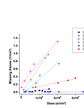
The results of this assessment are shown in Fig. 2, where the number of lost atoms vs. total dose per area is shown for all experiments. A linear fit is made for each case, and the slope directly provides the experimental knock-on cross section (since a small initial damage may be created before the first image is recorded some of the lines do not go through the origin). Two independent measurements were made for the 100kV case, but with a different dose rate ( and ). From the nearly identical result, we can exclude a dose rate effect within our experimental precision. Under 80 keV irradiation (not shown in Fig. 2), no vacancies were formed in pristine areas up to very high doses (beyond ).
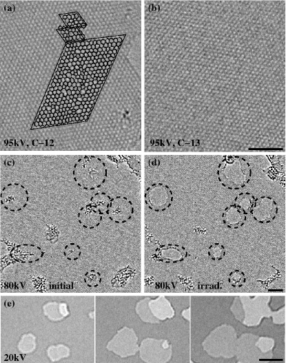
We begin our discussion by pointing out the clear difference between the and graphene membranes, and the differences between knock-on damage and a chemical etching effect. We find that the generation of vacancies within initially pristine, clean and defect free graphene membranes depends on the acceleration voltage, and also on the isotope composition ( vs. ). Fig. 3a,b shows graphene membranes of the two isotopes after exposure to 95 keV electrons, where the difference is most clearly visible. Hence, this must be a result of a direct collision between a beam electron and the carbon nucleus: Any chemical effect, or ionization damage, would not distinguish between and . As a side remark, we note that graphene membranes made from might provide an even better TEM sample support than ordinary single-layer graphene: The contrast background in HRTEM is identical, but the radiation damage rate is lower.
However, in contrast to the vacancy formation, the growth of extended holes in graphene Girit2009 is not predominantly a knock-on damage effect: We found that the growth rate of holes in graphene only weakly depends on the electron energy on a wide range of 20 keV to 100 keV: Holes still form and grow in graphene under 20 keV irradiation (Fig. 1c-e), and may even grow faster at low voltages (see supplementary information). This is in stark contrast to expectations from knock-on damage, where the threshold for displacing edge atoms is expected to be near 50 keV Kotakoski2011c . As shown in Fig. 3c-d, the extended holes always nucleate at contamination sites. We noticed that their growth rate is related to the vacuum levels, which varied in the range of to millibar, e.g. with use of the cold trap in the column, the time after insertion of the sample, or different outgassing rates of different sample holders. We conclude that this is beam-induced etching with residual water or oxygen in the system as described in Refs. Molhave2007 ; Barreiro2012 . Therefore, we count the formation of vacancies in initially clean and defect free areas as knock-on effect, but do not take into account the extended holes that nucleate at contamination sites.
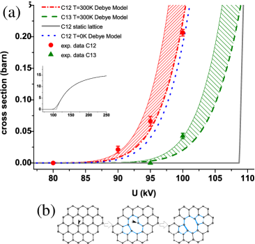
The analysis of our results culminates in the plot shown in Fig. 4. Here, each of the slopes from Fig. 2 provides one data point for a measured displacement cross section. The error bars indicate the statistical variation (standard deviation) in the data. Also shown in Fig. 4 are calculated curves from existing and new calculations that will be discussed below. For two curves, we show a shaded area between and the calculated cross section, since correlated sputtering of carbon atoms may increase the observed atom loss by up to a factor of two: After creation of a mono-vacancy by electron impact, one carbon atom is left with a dangling bond and a much lower emission threshold Krasheninnikov2005 ; Kotakoski2011c . Subsequent (and much more rapid) sputtering of this atom may effectively double the rate of atom loss (Fig. 4b). As a competing mechanism, two mono-vacancies that are created close to each other may combine and form a stable di-vacancy (since impacts of energetic electrons can rotate bonds in graphene Kotakoski2011 ; Kotakoski2011a , it is likely that exposure to the beam increases also the diffusivity of vacancies). In this case, the sputtering rate would not have to be doubled. Qualitatively, one would expect that correlated sputtering is dominant close to the threshold, while nearby mono-vacancies are more likely generated at higher electron energies (this is further discussed in the supplement). In any case, the resulting multi-vacancy configurations contain only very few undercoordinated carbon atoms, while the 3-coordinated atoms in the reconstructed configurations are expected to have an emission threshold similar to that of an atom in the pristine graphene sheet Kotakoski2011a . Another conceivable mechanism that might have an influence on the experimental results, namely the annealing of vacancies with mobile carbon adatoms, can not be dominant in our experiment as evidenced by the absence of a dose rate effect. Hence, we expect a rate of atom loss in-between and of the value calculated for pristine graphene.
The cross section for Coloumb scattering between an electron and a corresponding target nucleus was derived by Mott Mott1929 . McKinley and Feshbach have found an analytic expression for the Mott scattering cross section as a function of the maximum transferred energy W.McKinley ,
| (1) |
where is the atomic number of the target atoms, the Rydberg energy, the Bohr radius of the hydrogen atom, (electron velocity divided by the speed of light ), the mass of th electron and . represents the maximum transferred energy in the collision event and a threshold energy for atomic displacement. Without modifications, equation (2) is suitable to evaluate the total “knock-on” cross section for an atom at rest with a given ejection threshold energy. The curve from equation (2) (“static lattice” in Fig. 4), features a rather sharp onset of radiation damage with increasing acceleration voltage: The cross section is zero up to a well defined threshold (here 108 kV), and then rises to several barn (beyond all our measured values) only a few kV above this threshold. Changing the displacement threshold in the Mc-Kinley Feshbach formula predominantly shifts this curve sideways, but does not affect the sharp onset. Hence, independent of the free parameter this approximation is in clear contrast to our experiment, which shows a smooth onset of the damage cross section between 80 and 100 keV.
Remarkably, our data can be explained by considering the effect of the struck atom’s vibrations on its own displacement. While the effect has been discussed earlier Brown1959 ; Iwata ; Zag1983 , our measurement provides precise experimental evidence of this intriguing effect. In essence, it means that an atom that is struck by an electron while it happens to move parallel to the electron beam can obtain a higher maximum transferred energy than if it were static. For our calculation, we approximate the phonon distribution of the material in the framework of the Debye model. We use the Debye temperature calculated for out of plane vibrations in graphene of from Ref. Tewary2009 . Since depends on the speed of sound, it follows for the Debye temperature of that . We extract the distribution of atom velocities in the beam direction from the model, calculate the maximum transferred energy as a function of the atom velocity and electron energy , and obtain the weighted sum of the sputtering cross section numerically (see supplementary information). In other words, we still use the Mott scattering cross section, but we consider that the atom is not at rest initially. The threshold energy of was taken from first principles calculations Kotakoski2010 without any adjustments (Refs. Zobelli2007a ; Krasheninnikov2005 give similar values). With this value, the smooth onset of knock on damage between 80-100 keV is very well reproduced. For the first time, no adjustment to the calculated threshold energy is needed to explain the data, as was the case in previous studies Zobelli2007a ; Kotakoski2010 : Remarkably, the previous mismatch between theory and experiments was not due to inadequate calculations of , but because the effects of lattice vibrations on the elastic collision were not considered. Interestingly, the calculated curves are almost identical for the zero-kelvin and room-temperature case (Fig. 4, T=0 K and T=300 K curves). This implies that already the zero-point energy of the phonon modes is sufficient to explain the increased sputtering cross section as compared to the static lattice.
In summary, we have made an accurate measurement of atomic displacement cross sections for carbon atoms in single-layer graphene. The cross section smoothly rises from practically zero ( barn) at 80 keV to barn at 100 keV. In practice this means that 80 keV imaging of defect free graphene is easily possible, while already 100 keV TEM images might not represent the original configuration of a sample. A static lattice model is not sufficient to model the process, and the contribution of atomic motion adds significantly to knock-on damage cross sections near the threshold. The difference between and isotopes is detectable and further confirms the model. While the results on graphene will be important for HRTEM studies of this material and related ones (especially carbon nanotubes), the generalized insights to radiation damage mechanisms should be more generally applicable to any material where knock-on damage is important. Our results show that knock-on displacement cross sections can be modeled with high accuracy, if lattice vibrations are taken into account.
Acknowledgments: We acknowledge financial support by the German Research Foundation (DFG) and the Ministry of Science, Research and the Arts (MWK) of the state Baden-Württemberg within the Sub-Angstrom Low-Voltage Electron Microscopy project (SALVE). A.V.K. and J.K. acknowledge the support from the Academy of Finland through several projects. V.S. acknowledges EC grant No 266391 related to the project ELECTROGRAPH (FP7/2007-2013). S.R. acknowledges support by Korea WCU R32-2008-000-10082-0.
Supplementary information
I Supplementary experimental data
Figures 5-7 show additional image sequences and the analysis of defect
geometries with the number of missing atoms. Figs. 5 and 6 show the
radiation damage in graphene under 90 keV and
95 keV electron irradiation. For Fig. 6, it should be noted that
the extended hole that grows on the right-hand side of the image was
not taken into account (as discussed above, these holes nucleate at
contamination sites and grow via a beam-induced etching effect). The
sequence in Fig. 6 also shows two of the rare cases where a heavier
contamination atom is trapped in a vacancy (these are also counted
as a lost carbon atom). Fig. 7 shows the graphene
sample under 100 keV electron irradiation. The rate of atom loss
in this sample is significantly reduced compared to the
sample (compare Fig. 1 in the main article).


II Details of the displacement cross section calculation
The cross section for Coloumb scattering between an electron and a corresponding target nucleus has been derived by Mott in Mott1929 . McKinley and Feshbach have found an analytic expression for the Mott scattering cross section as a function of the maximum transferred energy W.McKinley .
| (2) |
where is the atomic number of the target atoms, the Rydberg energy, the Bohr radius of the hydrogen atom, the speed of light, ( velocity of the electron), the speed of light, the mass of the electron, and . represents the maximum transferred energy in the collision event and a threshold energy for atomic displacement. For an atom at rest, the maximum transferred energy in an elastic impact of the beam electron is given by expression
| (3) |
where is the kinetic energy of the electrons and the mass of the atomic nucleus. This expression is based on the (well justified) approximations that the atomic nucleus is much heavier than the electron (), and that its rest energy is much larger than the beam energy ().
The above expression is commonly used to calculate sputtering cross sections and thresholds. Our modified calculation now explicitly takes into account the fact that the target atom is not at rest due to the vibrations of the lattice. The importance of lattice vibrations as well as thermal effects for the displacement of atoms, irradiated with energetic particles was first suggested in 1959 by Brown and Augustyniak and subsequently mentioned in several publications Brown1959 ; Iwata ; Zag1983 . The effect is not obvious, because compared to the energy that is needed to displace an atom, its vibrational energy is very small. However, the fact that the atom is moving, significantly changes the transferred momentum and energy upon impact of the fast electron. By considering again a (relativistic) elastic collision between the beam electron and a moving target atom, the maximum transferred energy can be written as
| (4) |
with:
and
where is the initial velocity and
is the initial kinetic energy of the target atom. Here, refers
only to the component of the velocity that is normal to the graphene
plane, i.e. parallel to the electron beam.
We now consider how the cross section (eq. 2) is changed for the case of a moving target. The analytical expression for the original Mott Series Mott1929 ; Mott1932 (which is accurate up to the medium-Z elements McKinley1948 ) can be written as McKinley1948
| (5) |
with , being the scattering angle and the classical Rutherford scattering cross section:
If the target atom is at rest, the angular dependence of the transferred energy can be described as
For a moving target, the angular dependence of the transferred energy (with the atom initially moving) can be written as:
| (7) |
with and as given above. This can be rewritten and approximated as
| (8) |
with , where the approximation is valid for .
Hence, we obtain the same expression for as in equation (2), except that is replaced by the new : For the case of a moving target, we obtain
| (9) |
For our parameters (i.e. acceleration voltages, Debye temperature, atomic mass) we obtain , meaning that the approximation is well justified. The approximation can also be understood qualitatively, as that if the electron velocity is much higher than the atom velocity, the scattering angle is not significantly changed by the motion of the atom. Only for very low electron energies (on the order of 10 keV or below), one would need to consider a modification to equation 2 or 9.
The mean square velocity of an atom can be calculated within the framework of the Debye model to be Sinnemann1992
| (10) |
and it is Gaussian distributed (central limit theorem). Here, is the Boltzmann constant, the temperature, and the Debye temperature. The Debye model naturally contains a Bose-distribution for the phonon modes that also includes the quantum mechanical zero point motion for all vibration modes; meaning that the atoms are not at rest even at zero temperature. The normalized Gaussian distribution yields a probability for finding an atom with a velocity between and :
| (11) |
Now, that we have the probability distribution for the velocities (11) and using the scattering cross section (9) with the velocity-dependent expression for (4), we can integrate over all velocities weighted by their probability in order to obtain the total cross section:
| (12) |
This last integration step was done numerically. The heaviside step function ensures that only positive values for are summed up (equations 2 or 9 give non-physical, negative values if , which must be replaced by a zero scattering probability). The numerical integration was done over a range , providing the curves as shown in Fig. 4 of the main article.
III Correlated sputtering
Here, we briefly discuss the two competing mechanisms of correlated sputtering and the merging of nearby vacancies. After removing one carbon atom from the graphene lattice, in principle there are three atoms in an undercoordinated configuration. However, the configuration reconstructs to incorporate a carbon pentagon, which closes two of the open bonds and leaves only one atom undercoordinated Banhart2011 . The displacement threshold for this atom is only 14.7 eV Kotakoski2011c , compared to 22 eV for an atom in the pristine lattice. Our HRTEM observations show predominantly di-vacancies and (clustered) multi-divacancies, and exceptionally few single vacancies or other undercoordinated atoms.
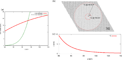
Two scenarios appear reasonable in the light of these observations. First, one might expect that the undercoordinated carbon atom is sputtered shortly after the initial vacancy is generated. In this case, the observed rate of atom loss would be twice the rate that is calculated for the pristine graphene lattice. Second, mono-vacancies that form in close proximity to each other may cluster and form di-vacancies without loosing additional atoms. As a starting point for quantifying these effects, we now compare (a) the probability (cross section) for sputtering the undercoordinated carbon atom, and (b) the probability for forming two mono-vacancies in close proximity. Fig. 8a shows the probabilites (as cross sections) for sputtering one undercoordinated atom compared to sputtering one carbon atom within a 1nm radius (120 atoms) of the original defect. From the graph it is clear that correlated sputtering will be dominant at lower electron energies and less significant at high energies, but quantification is difficult: Although clustering of defects is clearly observed, it is not clear at which rate or over which distances it occurs (the choice of 1nm as the example given above and in Fig. 8a is arbitrary). Fig 8b+c shows the analysis represented in a different way: It describes a radius over which sputtering an additional carbon atom from the pristine lattice would be equally likely as sputtering the undercoordinated atom at the vacancy. In our data (Fig. 4 of the main article), it indeed appears that the lowest energy data points ( at 90kV, at 100kV) correspond to correlated sputtering, while at 100kV does not. This is in agreement with the above discussion if we assume that mono-vacancies can cluster into divacancies over a distance of 1nm or less. In any case, we consider the range from 1x to 2x of the calculated cross section in the pristine lattice as a (material-specific) uncertainty in the model.
IV Chemical etching
In this section we expand our discussion of chemical etching in graphene under TEM imaging conditions. Although the focus of our analysis is on knock-on damage effects, it is also important to identify and separate other effects that are not knock-on damage. From a large number of experiments on graphene in the TEM, we conclude that the growth of extended holes is not predominantly an effect of knock on damage. This is particularly surprising since, under 80 keV irradiation, direct sputtering of edge atoms must also occur. However, the experiments show that it can not be the dominant mechanism.
Fig. 9a-c shows the typical formation and evolution of a hole in a graphene membrane under 80 keV electron irradiation. Initially, a contamination site is present (which may be attached to a defect site). Electron-energy loss spectroscopy and energy-dispersive x-ray spectroscopy indicated that silicon is a predominant contamination in our samples, and no other elements were detected. However, it can not be excluded that other reactive species are present in smaller quantities. In any case, we almost exclusively observe the formation of holes at sites with heavier (than carbon) contamination (Fig. 9a). The hole rapidly grows while the contamination is present and attached to the open edges (Fig. 9b), but eventually a hole with pristine (carbon-only) edges is formed (Fig. 9c). Such a hole can now be observed over extended times and up to high doses Girit2009 . It slowly grows under the beam. We have quantified the hole growth by measuring the hole perimeter as a function of dose, shown for part of our data in Fig. 9d. Hole formation and growth was observed in the same way also under 20kV HRTEM imaging Kaiser2011a .
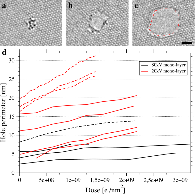
Several observations indicate that the hole growth is a chemical reaction with residual gas in the vacuum. The most significant one comes from the comparison of 20 kV and 80 kV data. Knock-on damage of graphene edge atoms should be strongly suppressed if not stopped entirely under 20kV irradiation, compared to 80kV Kotakoski2011c . However, we actually measured a slightly more rapid growth of holes under the 20kV beam. Second, we found that the growth rate of holes strongly varied in different experiments, in spite of similar irradiation conditions. Parameters that varied between these experiments were the sample holder, the pumping time after mounting the sample, or the use of the cold trap. In particular, we observed that hole growth slowed down after extended pumping (several hours after inserting the sample), compared to immediately after inserting the sample. We also noted one case of a leaking sample holder (contaminated o-ring) where hole growth was too rapid for achieving any high-resolution images. Indeed, exposure to a low-voltage electron beam under a controlled atmosphere of water or oxygen was used previously for a controlled cutting of carbon materials Yuzvinsky2005 . Etching of carbon with residual gas in the TEM column was also described by other authors Molhave2007 . Secondary displacements (e.g. displaced H atoms that, in turn, displace C atoms) also can not play a signifcant role, as again one would expect a clear dependence on acceleration voltage for this mechanism. In summary, we conclude that hole formation and growth depends on the contamination on the sample (which acts as a catalyst) and on the residual vacuum levels, and these effects dominate over the knock-on displacements under our experimental conditions.
V Description of the supplementary videos
Supplementary video S1: A side-by-side comparison of the and graphene sample under 95 keV electron irradiation, recorded under identical imaging conditions. One can clearly see the much more rapid decay of the sample in the electron beam. The total dose at the end of the image sequence is .
Supplementary video S2: A long image sequence showing a graphene membrane under 80 keV electron irradiation. No change can be detected within the pristine lattice area. The total dose at the end of the image sequence is .
Supplementary video S3: A long image sequence showing a graphene membrane under 80 keV electron irradiation (showing a larger area view as compared to video S2). No change can be detected within the pristine lattice area, but the formation of extended holes at the contamination spots is clearly evident. The total dose at the end of the image sequence is . In particular, holes start at the heavier (non-carbon) contamination, which appears to catalyze the reaction.
Supplementary video S4: Formation of defects in graphene under 100 keV electron irradiation. The total dose at the end of the image sequence is . A few seconds (less than 30s, total time of the sequence is ca. 1 hour) are missing after frames 10, 35, 91 and 132 as the focus was readjusted.
Supplementary video S5: Formation of defects in graphene under 100 keV electron irradiation (note that frames 120-177 are out of focus; frames 198-213 are recorded under inverse conditions i.e. atoms appear white). The total dose at the end of the image sequence is .
References
- (1) R. F. Egerton, P. Li, and M. Malac, “Radiation damage in the TEM and SEM.,” Micron (Oxford, England : 1993), vol. 35, pp. 399–409, Jan. 2004.
- (2) M. Haider, S. Uhlemann, E. Schwan, H. Rose, B. Kabius, and K. Urban, “Electron microscopy image enhanced,” Nature, vol. 392, no. 6678, pp. 768–769, 1998.
- (3) P. E. Batson, N. Dellby, and O. L. Krivanek, “Sub-ångstrom resolution using aberration corrected electron optics.,” Nature, vol. 418, pp. 617–20, Aug. 2002.
- (4) P. E. Batson, “Simultaneous STEM imaging and electron energy-loss spectroscopy with atomic-column sensitivity,” Nature, vol. 366, pp. 727–728, 1993.
- (5) U. Kaiser, D. A. Muller, J. L. Grazul, A. Chuvilin, and M. Kawasaki, “Direct observation of defect-mediated cluster nucleation.,” Nature materials, vol. 1, pp. 102–5, Oct. 2002.
- (6) D. A. Muller, L. F. Kourkoutis, M. Murfitt, J. H. Song, H. Y. Hwang, J. Silcox, N. Dellby, and O. L. Krivanek, “Atomic-scale chemical imaging of composition and bonding by aberration-corrected microscopy.,” Science, vol. 319, pp. 1073–6, Feb. 2008.
- (7) K. Suenaga, Y. Sato, Z. Liu, H. Kataura, T. Okazaki, K. Kimoto, H. Sawada, T. Sasaki, K. Omoto, T. Tomita, T. Kaneyama, and Y. Kondo, “Visualizing and identifying single atoms using electron energy-loss spectroscopy with low accelerating voltage,” Nature Chemistry, vol. 1, pp. 415–418, July 2009.
- (8) M. Bar Sadan, L. Houben, S. G. Wolf, A. Enyashin, G. Seifert, R. Tenne, and K. Urban, “Toward atomic-scale bright-field electron tomography for the study of fullerene-like nanostructures.,” Nano letters, vol. 8, pp. 891–6, Mar. 2008.
- (9) J. C. Meyer, S. Kurasch, H. J. Park, V. Skakalova, D. Künzel, A. Gross, A. Chuvilin, G. Algara-Siller, S. Roth, T. Iwasaki, U. Starke, J. H. Smet, and U. Kaiser, “Experimental analysis of charge redistribution due to chemical bonding by high-resolution transmission electron microscopy.,” Nature materials, vol. 10, pp. 209–15, Mar. 2011.
- (10) S. Iijima, “Helical microtubules of graphitic carbon,” Nature, vol. 354, no. 6348, pp. 56–58, 1991.
- (11) S. Iijima and T. Ichihashi, “Single-shell carbon nanotubes of 1-nm diameter,” Nature, vol. 363, pp. 603–605, June 1993.
- (12) H. W. Kroto, J. R. Heath, S. C. O’Brien, R. F. Curl, and R. E. Smalley, “C60: Buckminsterfullerene,” Nature, vol. 318, pp. 162–163, Nov. 1985.
- (13) K. S. Novoselov, A. K. Geim, S. V. Morozov, D. Jiang, Y. Zhang, S. V. Dubonos, I. V. Grigorieva, and A. A. Firsov, “Electric field effect in atomically thin carbon films.,” Science, vol. 306, pp. 666–9, Oct. 2004.
- (14) A. K. Geim and K. S. Novoselov, “The rise of graphene.,” Nature materials, vol. 6, pp. 183–91, Mar. 2007.
- (15) D. Pacile, J. C. Meyer, c. O. Girit, and A. Zettl, “The two-dimensional phase of boron nitride: Few-atomic-layer sheets and suspended membranes,” Applied Physics Letters, vol. 92, p. 133107, 2008.
- (16) K. S. Novoselov, D. Jiang, F. Schedin, T. J. Booth, V. V. Khotkevich, S. V. Morozov, and A. K. Geim, “Two-dimensional atomic crystals.,” Proceedings of the National Academy of Sciences of the United States of America, vol. 102, pp. 10451–3, July 2005.
- (17) F. Banhart, “Irradiation effects in carbon nanostructures,” Reports on Progress in Physics, vol. 62, p. 1181, 1999.
- (18) M. Lucas, “The threshold curve for the displacement of atoms in graphite: experiments on the resistivity changes produced in single crystals by fast electron irradiation at 15°K,” Carbon, vol. 1, pp. 345–352, 1964.
- (19) V. H. Crespi, N. G. Chopra, M. L. Cohen, A. Zettl, and S. Louie, “Anisotropic electron-beam damage and the collapse of carbon nanotubes.,” Physical review. B, Condensed matter, vol. 54, pp. 5927–5931, Aug. 1996.
- (20) B. W. Smith and D. E. Luzzi, “Electron irradiation effects in single wall carbon nanotubes,” Journal of Applied Physics, vol. 90, no. 7, p. 3509, 2001.
- (21) A. Krasheninnikov, F. Banhart, J. Li, A. Foster, and R. Nieminen, “Stability of carbon nanotubes under electron irradiation: Role of tube diameter and chirality,” Physical Review B, vol. 72, Sept. 2005.
- (22) A. Zobelli, A. Gloter, C. Ewels, G. Seifert, and C. Colliex, “Electron knock-on cross section of carbon and boron nitride nanotubes,” Physical Review B, vol. 75, pp. 1–9, June 2007.
- (23) K. Mø lhave, S. B. Gudnason, A. T. Pedersen, C. H. Clausen, A. Horsewell, and P. Bø ggild, “Electron irradiation-induced destruction of carbon nanotubes in electron microscopes.,” Ultramicroscopy, vol. 108, pp. 52–7, Dec. 2007.
- (24) J. H. Warner, F. Schäffel, G. Zhong, M. H. Rümmeli, B. Büchner, J. Robertson, and G. A. D. Briggs, “Investigating the diameter-dependent stability of single-walled carbon nanotubes.,” ACS nano, vol. 3, pp. 1557–63, June 2009.
- (25) D. Cherns, F. J. Minter, and R. S. Nelson, “Sputtering in the high voltage electron microscope,” Nuclear Instruments and Methods, vol. 132, pp. 369–376, 1976.
- (26) R. Egerton, R. McLeod, F. Wang, and M. Malac, “Basic questions related to electron-induced sputtering in the TEM,” Ultramicroscopy, vol. 110, pp. 991–997, July 2010.
- (27) R. F. Egerton, “The threshold energy for electron irradiation damage in single-crystal graphite,” Philosophical Magazine, vol. 35, pp. 1425–1428, May 1977.
- (28) W. Zag and K. Urban, “Temperature dependence of the threshold energy for atom displacement in irradiated molybdenum,” physica status solidi (a), vol. 76, no. 1, pp. 285–295, 1983.
- (29) V. Crespi, L. Benedict, M. Cohen, and S. Louie, “Prediction of a pure-carbon planar covalent metal.,” Physical review. B, Condensed matter, vol. 53, pp. R13303–R13305, May 1996.
- (30) H. Terrones, M. Terrones, E. Hernández, N. Grobert, J.-C. Charlier, and P. Ajayan, “New Metallic Allotropes of Planar and Tubular Carbon,” Physical Review Letters, vol. 84, pp. 1716–1719, Feb. 2000.
- (31) M. Lusk and L. Carr, “Nanoengineering Defect Structures on Graphene,” Physical Review Letters, vol. 100, Apr. 2008.
- (32) M. D. Fischbein and M. Drndic, “Electron beam nanosculpting of suspended graphene sheets,” Applied Physics Letters, vol. 93, p. 113107, Sept. 2008.
- (33) J. Kotakoski, A. Krasheninnikov, U. Kaiser, and J. Meyer, “From Point Defects in Graphene to Two-Dimensional Amorphous Carbon,” Physical Review Letters, vol. 106, p. 105505, Mar. 2011.
- (34) A. V. Krasheninnikov and F. Banhart, “Engineering of nanostructured carbon materials with electron or ion beams,” Nature Materials, vol. 6, no. 10, pp. 723–733, 2007.
- (35) J. C. Meyer, C. Kisielowski, R. Erni, M. D. Rossell, M. F. Crommie, and A. Zettl, “Direct imaging of lattice atoms and topological defects in graphene membranes,” Nano letters, vol. 8, no. 11, pp. 3582–3586, 2008.
- (36) U. Kaiser, J. Biskupek, J. C. Meyer, J. Leschner, L. Lechner, H. Rose, M. Stöger-Pollach, A. N. Khlobystov, P. Hartel, H. Müller, M. Haider, S. Eyhusen, and G. Benner, “Transmission electron microscopy at 20kV for imaging and spectroscopy.,” Ultramicroscopy, vol. 111, no. 8, pp. 1239–1246, 2011.
- (37) J. C. Meyer, C. O. Girit, M. F. Crommie, and A. Zettl, “Hydrocarbon lithography on graphene membranes,” Applied Physics Letters, vol. 92, p. 123110, 2008.
- (38) H. J. Park, J. Meyer, S. Roth, and V. Skákalová, “Growth and properties of few-layer graphene prepared by chemical vapor deposition,” Carbon, vol. 48, pp. 1088–1094, Apr. 2010.
- (39) C. O. Girit, J. C. Meyer, R. Erni, M. D. Rossell, C. Kisielowski, L. Yang, C.-H. Park, M. F. Crommie, M. L. Cohen, S. G. Louie, and A. Zettl, “Graphene at the edge: stability and dynamics.,” Science, vol. 323, pp. 1705–8, Mar. 2009.
- (40) J. Kotakoski, D. Santos-Cottin, and A. V. Krasheninnikov, “Stability of Graphene Edges under Electron Beam: Equilibrium Energetics vs. Dynamic Effects,” ACS Nano, p. 111222003752008, Dec. 2011.
- (41) A. Barreiro, F. Boerrnert, S. M. Avdoshenko, B. Rellinghaus, G. Cuniberti, M. H. Ruemmeli, and L. M. K. Vandersypen, “Transforming amorphous carbon into graphene by current-induced annealing,” Arxiv, p. 1201.3131, Jan. 2012.
- (42) J. Kotakoski, J. Meyer, S. Kurasch, D. Santos-Cottin, U. Kaiser, and A. Krasheninnikov, “Stone-Wales-type transformations in carbon nanostructures driven by electron irradiation,” Physical Review B, vol. 83, p. 245420, June 2011.
- (43) N. F. Mott, “The scattering of fast electrons by atomic nuclei,” Proceedings of the Royal Society of London Series A, vol. 124, no. 794, pp. 425–442, 1929.
- (44) W. McKinley and H. Feshbach, “The Coulob Scattering of Relativistic Electrons by Nuclei,” Phys. Rev., vol. 74, no. 12, pp. 1759–1763, 1948.
- (45) W. L. Brown and W. M. Augustyniak, “Energy, Orientation, and Temperature Dependence of Defect Formation in Electron Irradiation of n-Type Germanium,” J. Appl. Phys., vol. 30, no. 8, p. 1300, 1959.
- (46) T. Iwata and T. Nihira, “Atomic Displacement by Electron Irradiation in Pyrolytic Graphite,” J. Phys. Soc. Jpn, vol. 31, no. 6, 1971.
- (47) V. Tewary and B. Yang, “Singular behavior of the Debye-Waller factor of graphene,” Phys. Rev. B, vol. 79, pp. 1–5, Mar. 2009.
- (48) J. Kotakoski, C. Jin, O. Lehtinen, K. Suenaga, and A. Krasheninnikov, “Electron knock-on damage in hexagonal boron nitride monolayers,” Physical Review B, vol. 82, Sept. 2010.
- (49) N. F. Mott, “The polarisation of electrons by double scattering,” Proceedings of the Royal Society of London Series A, vol. 135, no. 827, pp. 429–458, 1932.
- (50) W. McKinley and H. Feshbach, “The Coulomb Scattering of Relativistic Electrons by Nuclei,” Physical Review, vol. 74, pp. 1759–1763, Dec. 1948.
- (51) T. Sinnemann, R. Job, and M. Rosenberg, “Reduction of the zero-phonon 57Fe Mössbauer fraction just above Tc in the (Bi,Pb)2Sr2Ca2Cu3O10 superconductor,” Phys. Rev. B, vol. 45, no. 9, pp. 1–4, 1992.
- (52) F. Banhart, J. Kotakoski, and A. V. Krasheninnikov, “Structural defects in graphene.,” ACS nano, vol. 5, pp. 26–41, Jan. 2011.
- (53) T. D. Yuzvinsky, A. M. Fennimore, W. Mickelson, C. Esquivias, and A. Zettl, “Precision cutting of nanotubes with a low-energy electron beam,” Applied Physics Letters, vol. 86, no. 5, p. 053109, 2005.