Huge local field enhancement in perfect plasmonic absorbers
Abstract
In this Letter we theoretically study the possibility of total power absorption of light in a planar grid modelled as an effective sheet with zero optical thickness. The key prerequisite of this effect is the simultaneous presence of both resonant electric and magnetic modes in the structure. We show that the needed level of the magnetic mode is achievable using the effect of substrate-induced bianisotropy which also allows the huge local field enhancement at the same wavelength where the maximal absorption holds.
pacs:
81.05.Xj, 78.67.Pt, 73.20.Mf, 42.25.Bs, 78.47.je, 78.30.-j, 42.50.StTotal absorption (TA) of light at a certain wavelength in a lossy layer located on a substrate implies simultaneous suppression of both reflection of the incident wave and transmission of this wave into the substrate. This effect has been applied in optical sensing and energy harvesting devices Luo1 ; Yu1 ; Sch1 ; Der1 ; Eme1 ; Polman . However, in the majority known optical absorbers the TA regime is not achievable and can be only more or less approached Azzam . In the microwave and mm wave ranges the TA was engineered exactly in the so-called Dallenbach absorber (see e.g. in Vin ) which comprises a metal substrate. In the optical range the TA was obtained in the so-called coherent perfect absorber using two incident waves Sci . In both these cases the absorber was a bulk lossy layer and the destructive wave interference in presence of two reflecting boundaries was used. Recently, the TA has been predicted for so-called perfect plasmonic absorbers (PPA) PPA1 ; PPA2 ; PPA3 . PPA is a very thin and optically dense planar grid of plasmonic nanoparticles (nanodisks or nanopatches) separated by an optically thin dielectric gap from a metal substrate. Planar grids of resonant particles can be homogenized using the surface averaging of their microscopic responses (see e.g. Hol2 ; Sim1 ). Such homogenized resonant grids presented as infinitesimally thin sheets of surface polarization were called metasurfaces or metafilms. The mechanism of the TA in known PPAs is still the destructive wave interference. The wave reflected from the metal substrate cancels out with that reflected from the metafilm PPA2 ; PPA3 . This cancellation becomes possible due to the resonant properties of the plasmonic grid.
In the present Letter we suggest a novel type of PPA with another mechanism of the TA and with an additional functionality. In our PPA the transmittance into the substrate is prevented even if the substrate is transparent and the reflectance is prevented in the absence of the second reflecting boundary. The TA is achieved due to the combination of the electric and magnetic modes in the structure. Additionally, our PPAs possess huge local field enhancement (LFE) in strongly subwavelength volumes. The effect of LFE is very important in numerous applications and has been recently widely studied (see e.g. Kim1 ; Tam1 ; Wat1 ; Mic1 ; Led1 ; Gri1 ; Rot1 ; Chall1 ). The combination of TA and LFE is very advantageous, e.g. for the surface enhanced Raman scattering (SERS). In many of SERS schemes the LFE holds in a targeted spatial region (e.g. at the nanopatterned surface of silver or gold) and results in the giant enhancement of the Raman radiation from this region Raman ; Raman1 . Both reflected and transmitted waves are parasitic signals whose presence hinders the detection of the Raman radiation from the targeted spatial region Raman ; Raman1 . Thus, for prospective SERS schemes it is advantageous to use PPAs (if they possess the LFE effect).
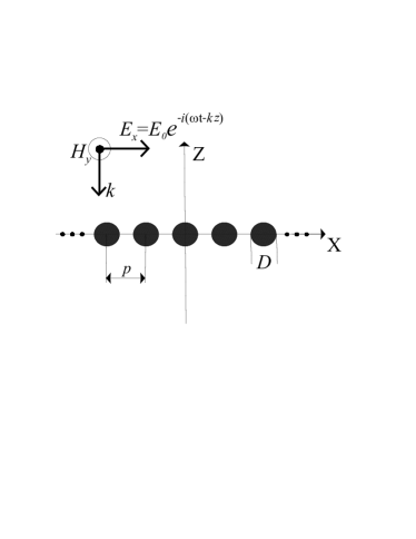
First, let us show that it is possible to achieve the TA in a metafilm without any substrate. Consider an optically dense planar array of particles possessing both electric and magnetic polarizabilities and located in free space. Alternatively, we can have in mind one electric dipole and one magnetic dipole per unit cell located in the grid plane. This planar array can be modelled as a metafim with both electric and magnetic surface polarizations Hol2 ; Sim1 . Let us show that the TA in the metafilm is achievable with realizable parameters describing its electromagnetic response. For simplicity the array is assumed to be isotropic in the -plane and a plane wave impinging normally to the array plane, see Fig. 1 (a). Then according to Hol2 ; Mo1 one can describe the response of the effective sheet by two surface susceptibilities and . The relationship between the electric and magnetic surface polarizations and the mean values of the electric and magnetic fields at the grid plane can be written as Hol2 ; Mo1 :
| (1) |
Here and are defined as the averaged values of electric and magnetic fields taken on two sides of the effective sheet, and are the electric and magnetic surface polarizations, respectively. Using the boundary conditions for such metafilms derived in Hol2 ; Mo1 , we obtain from (1):
| (2) |
Here and are complex reflection and transmission coefficients, respectively, and it is denoted: , , where is the free space wave number ( and are free space permeability and permittivity, respectively). From (2) it is easy to see that if electric and magnetic susceptibilities are, respectively, equal to:
| (3) |
Both required electric and magnetic polarizabilities are purely imaginary that is achievable if the electric and magnetic resonances of our particles coincide. This is definitely a realizable requirement i.e. the regime when the absorption coefficient equals to unity is possible. The key prerequisite is the resonant magnetic susceptibility (3-b) created in addition to the electric one (3-a). This is not problematic at microwaves, however for the visible frequency range becomes challenging. Therefore further we show how to engineer the surface magnetic polarization for a metafilm without any magnetic susceptibility in this range. Moreover we show how to combine the TA together with the LFE obtaining this way a new functionality of PPA layers.
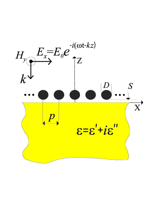
The proposed PPA depicted in Fig. 1 (b) comprises an optically dense planar grid (e.g. a square array with the period ) of plasmonic nanospheres with the optically small diameter located over the surface of a strongly refracting half-space at a very small distance from it. In previously known PPAs plasmonic nanoparticles were thin tablets and the plasmonic grid formed the effective plane of reflection clearly distinct from a metal interface. Thus, the reflection in previously known PPAs was prevented due to the wave interference PPA2 whereas the transmittance was prevented due to the total reflectance of the metal substrate. In the present case the distance between the lower edges of nanospheres and the semiconductor surface is much smaller than and the geometry does not contain two effective reflection planes. The only reflection plane is the interface to which we refer our metafilm. The resonant magnetic polarization in our metafilm arises due to the so-called substrate-induced bianisotropy which was theoretically revealed and studied in Mo1 for arrays of resonant electric dipoles located on top of a half-space with high refractive index. For the visible range this implies a semiconductor substrate. In our case both reflection and transmission are prevented to the balance of the effective electric and magnetic polarizations of a metafilm. However, the most important effect is the regime of LFE i.e. the new suggested functionality of our PPA.
| (nm) | (nm) | (nm) | |
|---|---|---|---|
| (a-Si substrate) | |||
| (Silver spheres) |
In this paper we consider the normally incident plane wave and a free space gap . This is done for simplicity and to stress that the wave interference does not play any role. The same functionality can be shown for obliquely incident waves and for nanospheres located on a 1-3 nanometer thick intermediate layer with low refractive index. Although small plasmonic nanospheres possess only the electric dipole response, the presence of the high-contrast substrate leads to the excitation of the magnetic mode Mo1 . This fact is illustrated by Fig. 2 which also shows the LFE in the proposed scheme of the PPA. Fig. 2 is the color map of the electric field amplitude in the central cross section of a unit cell. This field distribution was simulated at the wavelength of maximal power absorption (MPA) achievable for this structure (). Dimensions of the structure and parameters of the used materials at are summarized in Table 1, see also Fig. 1 (b). The complex permittivities of Ag and a-Si were taken from El-K and Si , respectively. Since is within the range of the plasmon resonance of the nanosphere it acquires a large dipole moment. In accordance with the quasi-static image principle calculating the near field one can replace the substrate by an image of the nanosphere. The local field is enhanced mainly in the gap between the nanosphere and the substrate (see Fig. 2). This is similar to the operation of a nanoantenna Tam1 . This is not a usual situation since the hot spot in the gap arises for the horizontal polarization of the incident field. However a similar mode has been known for non-symmetric dimers of plasmonic spheres Klimov . In this dimer the mode analogous to our one is characterized by a strong local polarization of both spheres near their internal edges. In our case the role of the second sphere is played by the image of the first one created by the substrate. To obtain this regime we need a strong optical contrast between two half-spaces and a sufficient curvature of the nanoparticle.
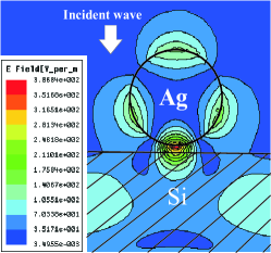
Fig. 2 also illustrates the substrate-induced bianisotropy. Since the gap is very small a noticeable part of the hot spot turns out to be located inside the semiconductor. This local polarization of the substrate is concentrated in a nanovolume at a noticeable distance from the effective dipole of the nanosphere. One can check that at these two effective dipoles (they are both horizontally directed) have opposite phases. The unit cell of the proposed PPA is then equivalent to a pair of electric and magnetic dipoles. Due to the optical smallness of the cell both these dipoles can be referred to the interface. After the homogenization the structure becomes an effective sheet of resonant electric and magnetic surface polarizations. Whereas the LFE in the PPA results from the curvature of the nanoparticle, the TA can be explained as we have done above – using the homogenization model.
Using the same model as in Mo1 three effective tangential susceptibilities per unit area of the metafilm can be introduced by relations:
| (4) |
Here and are the electro-magnetic and magneto-electric surface susceptibilities, respectively. Due to the reciprocity we have , and only two susceptibilities remain in (4). Using boundary conditions derived in Mo1 we relate the complex reflection and transmission coefficients and with these susceptibilities and obtain the retrieval formulas:
| (5) |
The solution corresponding to the total absorption when and is evident:
| (6) |
Imaginary electric susceptibility in (6) is achievable exactly and corresponds to the maximum of electric losses in the metafilm. Imaginary magneto-electric susceptibility, on the contrary, corresponds to the absence of magneto-electric losses Serd . Strictly speaking the TA regime corresponding conditions (6) is an idealization: one can hardly create a metafilm with lossless electro-magnetic (magneto-electric) response. However, one can approach the target conditions (6) very closely. We refer to this regime as to that of maximal power absorption.
| susceptibility | ||
|---|---|---|
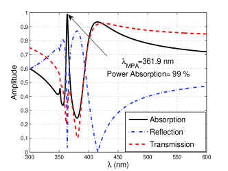
In our simulations we used both options of the HFSS package (the incident plane wave and the wave port) thoroughly checking the convergence. Moreover, we have reproduced the same results using the CST Studio software. Reflection, transmission, and absorption coefficients of this PPA versus frequency are plotted in Fig. 3. Using simulated and coefficients (amplitudes and phases) and substituting these data into (5) we have retrieved the corresponding electric and electro-magnetic susceptibilities. The target susceptibilities (6) and those retrieved for the proposed PPA at the wavelength are presented for comparison in Table 2. For spheres with nm over the a-Si substrate this disagreement between ideal and retrieved susceptibilities is minimal over all possible and . Further optimization is possible varying and .
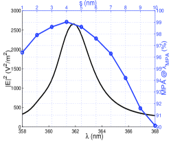
In Fig. 4 the line with circles shows the dependency calculated for every at the corresponding (for increasing from 1 to 10 nm the wavelength of MPA decreases from 381 to 358 nm). The resonance of the local field intensity normalized to that of the incident wave calculated at the brightest point of the hot spot is illustrated by the black line without circles in Fig. 4 for the optimal height nm. The effect of the maximal LFE holds exactly at the same wavelength as that of MPA nm. The same observation refers to other values of .
In this Letter we have theoretically demonstrated a possibility of almost total absorption in an optically dense planar grid of plasmonic nanoparticles over a transparent substrate. We have shown that this absorption does not result from the destructive wave interference as in previously known PPAs. The effect holds due to the balance of the electric and magnetic polarizations whereas the last one results from the substrate-induced bianisotropy. Moreover, this absorption is accompanied by a huge local field enhancement. This new functionality is granted by an effect similar to the LFE in plasmonic nanoantennas. We have checked by numerous simulations that this huge LFE does not hold for arrays of nanotablets, semi-spheres and other particles without curvature of the lower part. We have found that the larger is this curvature the stronger is the LFE. Though in the present paper the gap between the Ag nanospheres and the a-Si substrate is assumed to be filled with free space, this is not critical. Similar results can be obtained for spheres located in a dielectric medium over another semiconductor substrate. Alternatively, nanoparticles can be located in free space on a very thin dielectric layer. Local field intensity enhancement that we have revealed above (which is typical for many SERS schemes with nanoantennas) can be once more increased in arrays of touching nanopspheres due to collective effects Pendry ; Shalaev . This modification of the PPA can be probably done without the damage for the MPA regime.
Finally, we want to thank Prof. Sergei Tretyakov and Dr. Pavel Belov for clarifying and fruitful discussions.
References
- (1) C. Luo, A. Narayanaswamy, G. Chen, and J. D. Joannopoulos, Phys. Rev. Lett. 93, 213905 (2004).
- (2) Z. Yu, G. Veronis, S. Fan, and M. L. Brongersma, Appl. Phys. Lett. 89, 151116 (2006).
- (3) D. M. Schaadt, B. Feng, and E. T. Yu, Appl. Phys. Lett. 86, 063106 (2005).
- (4) D. Derkacs, S. H. Lim, P. Matheu, W. Mar, and E. T. Yu, Appl. Phys. Lett. 89, 093103 (2006).
- (5) K. Emery, Semicond. Sci. Technol. 18, 228 (2003).
- (6) H. A. Atwater and A. Polman, Nature Mat. 9, 205 (2010).
- (7) R. M. A. Azzam, E. Bu-Habib, J. Casset, G. Chassaing, and P. Gravier, Appl. Optics 26, 719 (1987).
- (8) K. J. Vinoy, R. M. Jha, Radar Absorbing Materials: From Theory to Design and Characterization, Kluwer: Boston, USA, 1999.
- (9) W. J. Wan, Y. D. Chong, L. Ge, H. Noh, A. D. Stone, and H. Cao, Science 331, 889 (2011).
- (10) N. Liu, M. Mesch, T.s Weiss, M. Hentschel, and H. Giessen, Nano Lett. 10, 2342 (2010).
- (11) M. Pu, C. Hu, M. Wang, C. Huang, Z. Zhao, C. Wang, Q. Feng, and X. Luo, Opt. Expr. 19, 17413 (2011).
- (12) M. K. Hedayati et al. Adv. Mat. 23, 5410 (2011).
- (13) C.L. Holloway, M.A. Mohamed, E.F. Kuester, and A. Dienstfrey, IEEE Trans. Electromagn. Compat. 47, 853 (2005).
- (14) C. R. Simovski, J. Opt. 13, 013001 (2011).
- (15) S. Kim et al., Nature (London) 453, 757 (2008).
- (16) T. H. Taminiau et al., Nat. Photon. 2, 234 (2008).
- (17) K. Watanabe et al., Chem. Rev. 106, 4301 (2006).
- (18) X. Michalet et al., Science 307, 538 (2005).
- (19) K.W. D. Ledingham, P. McKenna, and R. P. Singhal, Science 300, 1107 (2003).
- (20) D. G. Grier, Nature (London) 424, 810 (2003).
- (21) B. Rothenhausler and W. Knoll, Nature (London) 332, 615 (1988).
- (22) W. A. Challenger et al., Nat. Photon. 3, 220 (2009).
- (23) E. C. Le Ru and P. G. Etchegoin, Principles of Surface-Enhanced Raman Spectroscopy and Related Plasmonic Effects, Elsevier: Oxford, UK, 2009.
- (24) Surface-Enhanced Raman Scattering, Physics and Applications, K. Kneipp, M. Moskovits, and H. Kneipp, Eds., Springer: Berlin– Heidelberg–New York, 2006.
- (25) M. Albooyeh and C. Simovski, J. Opt. 13, 105102 (2011).
- (26) I. El-Kady, M. M. Sigalas, R. Biswas, K. M. Ho, and C. M. Soukoulis, Phys. Rev. B 62, 15299 (2000).
- (27) A. S. Ferlauto, G. M. Ferreira, J. M. Pearce, C. R. Wronski, R. W. Collins, X. Deng, and G. Ganguly, J. Applied Phys. 92, 2424 (2002).
- (28) V. V. Klimov and D. V. Guzatov, Phys.Rev. B 75,024303 (2007).
- (29) A. Serdyukov, I. Semchenko, S. Tretyakov, and A. Sihvola, Electromagnetics of Bi-anisotropic Materials: Theory and Applications, Gordon and Breach Science: Amsterdam, The Netherlands, 2001.
- (30) F.J. Garcia-Vidal and J.B. Pendry, Phys. Rev. Lett. 77, 1163 (1996).
- (31) D. A. Genov, A. K. Sarychev, V. M. Shalaev, and A. Wei, Nano Lett. 4, 153 (2004).