Ambipolar transport in bulk crystals of a topological insulator by gating with ionic liquid
Abstract
We report that the ionic-liquid gating of bulk single crystals of a topological insulator can control the type of the surface carriers and even results in ambipolar transport. This was made possible by the use of a highly bulk-insulating BiSbTeSe2 system where the chemical potential is located close to both the surface Dirac point and the middle of the bulk band gap. Thanks to the use of ionic liquid, the control of the surface chemical potential by gating was possible on the whole surface of a bulk three-dimensional sample, opening new experimental opportunities for topological insulators. In addition, our data suggest the existence of a nearly reversible electrochemical reaction that causes bulk carrier doping into the crystal during the ionic-liquid gating process.
pacs:
73.25.+i, 73.20.At, 72.20.My, 73.30.+yI Introduction
Three-dimensional (3D) topological insulators (TIs) are characterized by a novel topological order Moore ; Fu-Kane ; Roy ; QHZ which dictates the appearance of spin-filtered massless Dirac fermions on the surface.RMP_TI_10 ; Moore_Nature10 ; Qi_RMP11 To experimentally address the peculiar physics of 3D TIs, it is desirable to access the Dirac point of the surface state (SS).RMP_TI_10 ; Moore_Nature10 ; Qi_RMP11 This is relatively easy with the surface-sensitive spectroscopies such as the angle-resolved photoemission Hsieh_Nature08 ; NishidePRB10 ; Xia_Nphys09 ; SatoPRL10 ; Hiroshima_TBE_PRL10 ; ChenPRL10 ; Xue-NatCom ; Arakane_NComm12 and the scanning tunneling microscope,HanaguriPRB10 ; PCheng_PRL10 but it is more challenging for the bulk-sensitive transport experiments because the chemical potential is always pinned to the bulk bands (including the impurity band) in real materials. To tune the chemical potential to a desirable position for transport experiments, two approaches have been employed: one is the tuning of the chemical compositions upon synthesizing crystals,HorPRB09 ; RenPRB10 ; Taskin_BSTS_PRL11 ; Ren_BSTS_PRB11 ; Ren_Cd_PRB11 ; Jia_PRB11 and the other is the gating to control the surface carriers.ChenJ_PRL10 ; Steinberg_NL10 ; CheckelskyPRL11 ; Kong_NNano11 ; Yuan_NL11 Among the latter approach, the electric-double-layer gating (EDLG) method is a promising new technique Yuan_NL11 to allow application of a large electric field.Dhoot
In the EDLG configuration, either cations or anions in a liquid electrolyte are accumulated near the surface of a sample by application of an electric field, and they form an electric double layer which generates a very strong electric field locally on the surface. This leads to the induced surface carrier density of as high as 1015 cm-2.Dhoot Such a large tunability of the surface carrier density is the merit of the EDLG method. In the context of TIs, Yuan et al. showed Yuan_NL11 that the EDLG method allows an ambipolar doping control in ultrathin films of Bi2Te3; however, the surface state was obviously gapped in the ultrathin films used in Ref. Yuan_NL11, , and consequently the transport properties were likely to be dominated by the bulk state. In the present paper, we show that the EDLG method can achieve ambipolar transport even in bulk single crystals, if one uses the highly bulk-insulating Bi2-xSbxTe3-ySey (BSTS) system.Taskin_BSTS_PRL11 ; Ren_BSTS_PRB11 In our experiment, the control of the chemical potential was possible on the whole surface of a bulk 3D sample, opening new experimental opportunities for TIs. In addition, our data suggest that the chemical potential is moving not only at the surface but also in the bulk, possibly due to a nearly reversible electrochemical reaction to cause apparent bulk doping during the EDLG process.
II Sample Preparations and measurements
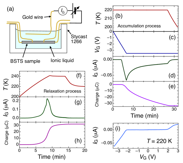
A series of BSTS single crystals were grown by a modified Bridgman method.Taskin_BSTS_PRL11 ; Ren_BSTS_PRB11 Six gold wires were attached to each sample by a spot welding technique, and magnetotransport measurements were performed by a conventional ac six-probe method by sweeping the magnetic field between 9 T. An electrically insulating cup made of Stycast 1266 was used as a sample container, in which the sample with gold wires was submerged into an ionic liquid (IL) electrolyte, as schematically shown in Fig. 1(a). We used a specially purified ionic liquid [EtMeIm][BF4] as the electrolyte.IL As the gate electrode, an additional piece of gold wire was dipped into the IL without touching the sample. In this paper, we adopt the convention of defining the gate voltage by taking the sample as the reference point, as was done in most of the previous works. In this convention, -type carriers are supposed to be doped to the surface when a positive gate voltage is applied.
The gate voltage was applied in the following procedure: first, the temperature of the sample was stabilized at 220 K; then, the gate voltage was swept slowly, and the temperature was kept at 220 K for at least 10 min after the voltage reached the set value; finally, the sample was cooled down slowly. When changing the gate voltage, we cycled the above procedure. Figures 1(b)-1(e) show an example of the history of , , gate current , and the accumulated charge, during the procedure for the target of V. With the IL used in the present experiment, gate current was never detected at temperatures below 200 K, even when the gate voltage was changed. This is because when the IL solidifies, ions are not mobile at all.
The accumulated ions can be released when the gate voltage is set to zero and the system is warmed up to 220 K. Such a relaxation process from = V is shown in Figs. 1(f)-1(h). One can see that the amount of released charge [32 C in Fig. 1(h)] is comparable to that of the accumulated charge [34 C in Fig. 1(e)]. The small difference between the released and accumulated charge is probably an indication of an irreversible electrochemical reaction during the gating processes at a high gate voltage. In the above example, the total surface area of the sample was 13.4 mm2, so that the 32 C of charge accumulated on the surface corresponds to the accumulated ion density of 1.6 cm-2 and the capacitance of the unit area 80 F cm-2, which is comparable to that previously reported for EDLG.YuanZnO Figure 1(i) shows vs curve at 220 K, which indicates that there is a threshold of 2 V below which little current flows, suggesting that the ions are not mobile below this threshold voltage; similar behavior was previously reported for a different IL.Ueno The origin of this behavior is currently not clear, but it may well be a characteristic of the ionic liquid used here. Also, it was difficult to obtain reproducible results of the transport properties for between 2 and 3 V, probably because the formation of the electric double layer is unstable in this gate-voltage region. Therefore, we closely measured the transport properties only in the range of V and = 0 V.
III EDLG experiment on single crystals
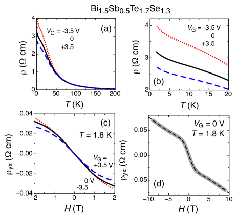
First, we show the results of the EDLG experiments on Bi1.5Sb0.5Te1.7Se1.3, which is currently one of the most bulk-insulating TI materials. Taskin_BSTS_PRL11 ; Ren_BSTS_PRB11 Figure 2(a) shows the temperature dependences of the resistivity with the gate voltage () of , 0, and +3.5 V. Even though this is a bulk single crystal, at low temperatures presents a clear change upon application of ; namely, below 50 K, changes with changing , and it tends to decrease (increase) for positive (negative) . Figure 2(b) magnifies this change for 20 K. Figure 2(c) shows the magnetic-field dependences of the Hall resistivity, . The sign of the charge carriers remains negative in this sample, although a significant non-linearity suggests the coexistence of surface and bulk conduction channels. Note that the surface conduction in TIs can involve both the topological surface states and topologically-trivial two-dimensional electron-gas (2DEG) states that appear as a result of band bending. Bianchi In the present experiment, when the gate voltage is applied, the 2DEG states are most likely contributing to the conduction alongside of the topological surface states. Unfortunately, we have not been able to elucidate the contributions of the topological and non-topological surface states because no Shubnikov-de Haas (SdH) oscillation has been observed in our gated samples. (To successfully separate the contributions of the two, detailed information obtained from SdH oscillations is necessary.Taskin_BSTS_PRL11 ; Taskin_MBE ) We therefore make no claim of the composition of the surface carriers in the present paper.
In Fig. 2(c), one can see a clear tendency that both the absolute value of and the slope of decrease upon increasing from to +3.5 V; this means that the apparent electron concentration increases with increasing . Since -type carriers are expected to be doped when a positive is applied, the present observation can be understood as a natural consequence of the EDLG. The nonlinear -dependence observed in is useful for gaining insights into the respective roles of bulk and surface transport channels, because its analysis based on a simple two-band model RenPRB10 gives a crude idea about the relevant transport parameters. For example, the data at = 0 V give the following estimate based on the fitting shown in Fig. 2(d): For the bulk channel, the bulk resistivity 3 , the bulk carrier density 9 1016 cm-3, and the bulk mobility 30 cm2/V s; for the surface channel, the sheet resistance 8 , the surface carrier density 2 1012 , and the surface mobility 5 103 cm2/V s. In this fitting, the constraint imposed by the presence of sharp kinks at 1 T helps reduce the ambiguity in the fitting parameters, and in fact, the three parameters, , , and , are in reasonable agreement with our previous transport studies of BSTS involving SdH oscillations.Taskin_BSTS_PRL11 ; Ren_BSTS_PRB11 The large value of would imply that the SdH oscillations be observed, but we did not observe any SdH oscillations in this sample; this is possibly because the surface chemical potential (and hence ) is not very uniform throughout the sample and the SdH oscillations with various different frequencies add up to smear visible oscillations.
The above result of the two-band analysis suggests that the surface contribution in the total conductance was only 1%, which is reasonable because the measured sample had a considerable thickness of 332 m. Nevertheless, if one looks at the EDLG effect in resistivity [Figs. 2(a) and 2(b)], one notices a very puzzling fact: for the negative of V, the number of surface electrons are expected to be reduced and indeed, the slope of gets larger; however, the resistivity increase is as much as 25%. Since the surface contribution in the total conductance is only 1%, even when the surface conduction is completely suppressed by EDLG, one can expect an increase in of 1% at most, as long as the bulk channel is not affected by EDLG. Therefore, the observed large increase in strongly suggests that the bulk channel must also be affected by EDLG. Indeed, the data shown in Fig. 2(c) presents a clear change in the slope at high fields for different , which implies that not only but also is changing. To corroborate this inference, the two-band analyses of the data at finite suggests that the bulk carriers decreases (increases) by 5% (10%) for of V ( V).
It is very surprising that the EDLG affects the density of bulk carriers by a noticeable amount in a sample as thick as 332 m, but our transport data can hardly be understood if one does not accept this possibility. Given that the electric field generated by 1 1015 cm-2 of ions on the surface is shielded in less than 100 nm,penetration the only possibility is that some bulk doping into the BSTS sample is taking place during the EDLG process. In this respect, the slow time scale of the change in the measured current during the EDLG process seems to support the idea that some electrochemical reaction is taking place.
In passing, we note that we have not successfully measured SdH oscillations in any of the gated samples. This is likely to be due to an inhomogeneous distribution of the local electric field (which is conceivable because our samples have a lot of macroscopic terraces on the surface) or some chemical degradation of the surface caused by the ionic-liquid gating. Hence a more definitive analysis of the transport data beyond the simple two-band analysis is currently unavailable. Nevertheless, the bulk doping due to the EDLG seems to be an inevitable conclusion of our result.
IV Ambipolar transport in single crystals
It was recently found Arakane_NComm12 that the position of the chemical potential with respect to the Dirac point of the SS is tunable within the bulk band gap in BSTS when one follows a particular series of and that were identified in Ref. Ren_BSTS_PRB11, . In particular, the chemical potential was found to be close to both the Dirac point of the SS and the middle of the bulk band gap in BiSbTeSe2. Therefore, for our EDLG experiment, to maximize the possibility of achieving ambipolar transport, we mainly measured the BiSbTeSe2 system. (The gating data shown in Fig. 1 were taken during the experiment on the BiSbTeSe2 sample reported below.)
| Experiment | ( cm) | (cm3/C) | |
|---|---|---|---|
| order | (V) | at 1.8 K | at 1.8 K |
| 1 | 0 | 13.8 | |
| 2 | 15.7 | ||
| 3 | 14.9 | 699 | |
| 4 | 15.2 | 165 | |
| 5 | 0 | 12.4 | |
| 6 | 10.9 | ||
| 7 | 14.2 | 289 |
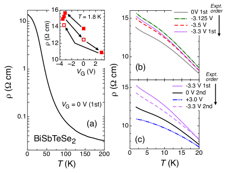
Figure 3(a) shows the temperature dependence of the resistivity of a BiSbTeSe2 single crystal before applying the gate voltage. One can see that exceeds 10 cm at low temperature, testifying to a high quality of this sample. As was the case with Bi1.5Sb0.5Te1.7Se1.3, at low temperatures we observed clear change in upon application of [Figs. 3(b) and 3(c)] even though this is a bulk single crystal. However, it also turned out that the transport properties do not completely recover after cycling . To illustrate the situation, we show in Table I the measured transport properties at 1.8 K for various values of in the order of the measurements. As one can see in this table, the transport properties for = 0 were measured twice, before and after applying = V; also, there are two different data for = V, which were taken before and after = V was applied. In both cases, the resistivity decreased after a high voltage was applied. Such a decrease in resistivity after application of a high voltage was also observed in other samples, so it appears to be an unavoidable effect in BSTS crystals; this is probably due to some irreversible electrochemical reaction taking place in the bulk, which gradually spoils the bulk-insulating property. However, as one can see in the inset of Fig. 3(a), a large part of the change in resistivity in response to is reversible. This reversible part of the change is consistent with the picture that the number of -type carriers increases with positive and decreases with negative due to the EDLG effect.
An interesting feature in our resistivity data is that the resistivity value presents a maximum around V [see inset of Fig. 3(a) and also Fig. 3(b)]; namely, the resistivity is smaller at of V compared to that at V, despite the overall trend that negative voltage increases . In fact, when the system is in the -type regime, a more negative value would lead to a smaller number of -type carriers, and one would expect the resistivity to increase; the opposite behavior observed for V suggests that the system is changing from -type to -type. To confirm this possibility, one must look at the Hall data.
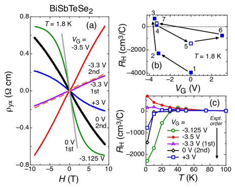
Figure 4(a) shows how the behavior of changes with . Initially, at = 0 V (first) and at V, the charge carriers are clearly -type, but the carriers become -type at large negative values of and V. This is a signature of an ambipolar transport in a bulk crystal, and confirms the idea that the sign change of charge carriers takes place between = and V. As noted above, the apparent maximum in the resistivity near V is consistent with this interpretation. The -type doping is recovered when was set to 0 V again, and the slope of was found to decrease with increasing up to V, suggesting an increase in the -type carriers, as expected.
It should be noted that we observed the sign change in this sample again after setting to V and then bringing it back to V, as shown by a broken line in Fig. 4(a). Thus, the sign change of the carriers is obviously reproducible. By defining the Hall coefficient as the slope of at low field, we summarize the gate-voltage dependences of in Fig. 4(b). One can see that the sign change in is reproducibly observed, although the exact value of at a given shows a history dependence.
The temperature dependences of for various measured in the successive five experiments [Fig. 4(c)] indicate that the ambipolar transport is observed only below 30 K where thermal activations of bulk carriers are negligible. Since the experiment on Bi1.5Sb0.5Te1.7Se1.3 discussed in the previous section indicated that the carrier densities in both the bulk and surface transport channels are changing with EDLG, it is important to elucidate whether the sign change of the carriers observed in BiSbTeSe2 is occurring in the bulk or on the surface, or both. To infer the origin of the sign change, we have analyzed the data for various values of with the simple two-band model.
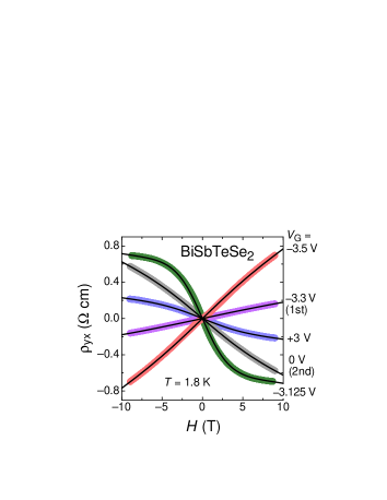
The results of the two-band fitting are summarized in Fig. 5 and Table II. For example, the fitting to the data at = 0 V shown in Fig. 5 gives the following crude estimate for the transport parameters: For the bulk channel, 13 cm, 1 cm-3, and 40 cm2/V s; for the surface channel, = 30 k, 2 cm-2, and 1 cm2/V s. Here, (= 181 m) is the thickness of the sample and the sign of charge carriers is negative for both the bulk and surface channels. Given that the chemical potential is very close to the Dirac point in BiSbTeSe2, it seems that the estimate of the surface carrier density indicated in this analysis is reasonable, in spite of the weakness of the non-linearity in . With the above parameters, the contribution of the surface channel to the total conductance is calculated to be 2%.
| Bulk carrier | Surface carrier | |||
|---|---|---|---|---|
| (V) | density (cm-3) | (cm2/Vs) | density (cm-2) | (cm2/Vs) |
| 1016 | 12 | 1011 | 1.2 103 | |
| 0 | 1016 | 38 | 1011 | 1.0 103 |
| 1016 | 21 | 1011 | 2.0 103 | |
| 5.0 1016 | 8 | 1.6 1011 | 4.6 102 | |
| 9.8 1015 | 42 | 1.8 1011 | 8.4 102 |
Looking at the results of the two-band analyses of the data at finite , one can see that the Hall data strongly suggests that both the bulk and surface carriers change sign simultaneously at V. Indeed, we found that it is impossible to fit the data for V by assuming that only one of the two channels changes sign. Therefore, it appears that in the present EDLG experiment the chemical potential is swung from the -type regime to the -type regime not only on the surface but also in the bulk. Most likely, what is happening in the bulk at negative is compensation due to electrochemical -type doping, which eventually overwhelms the preexisting -type bulk carriers.
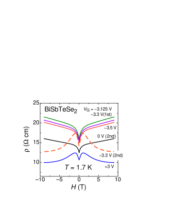
Finally, we show in Fig. 6 the magnetoresistance (MR) data for various values. Obviously, the data present the weak antilocalization (WAL) effect at low fields;WAL1 ; WAL2 ; Taskin_MBE since the WAL effect is a signature of two-dimensional transport and is not usually observed in bulk TI crystals dominated three-dimensional transport, the MR data give additional evidence for a sizable contribution of the surface transport to the total conductance. At the same time, this WAL effect makes it difficult to examine the consistency of the parameters obtained from the two-band analysis of in the MR data. Also, the behavior of MR qualitatively changed after the application of = V, the origin of which is not clear at the moment. Since the MR is too complicated and not very reproducible, we did not try to make a detailed analysis.
V Discussion
It is important to mention that there are missing charges in our EDLG experiment; namely, the total amount of charge induced by gating in the sample is much smaller than the total amount of ions accumulated on the surface. For example, in the case of BiSbTeSe2, the total amount of accumulated charges measured by the current is 34 C, which corresponds to the ion density on the surface of 1.6 1015 cm-2. On the other hand, the change in the surface carrier density in BiSbTeSe2 was 4 1011 cm-2 and its bulk carrier density changed by less than 1 1017 cm-3, which amounts to the total charge of less than 20 C. Therefore, obviously the gating is not very efficiently performed. In this regard, the doping control of the surface carriers in the present experiment is similar to another EDLG experiment on Bi2Te3 thin film,Yuan_NL11 where 7 1011 cm-2 of surface carriers were doped with V. For other materials, the amount of surface carrier doping by EDLG is of the order of 1013–1015 cm-2, Dhoot ; YuanZnO ; Ye_PNAS11 ; EndoAPL10 and thus the electric-field effect on Bi-based topological insulators appears to be exceptionally ineffective.note
The mechanism to cause these missing charges is not clear at the moment, but we speculate that some electrochemical redox reaction involving adsorbed molecules on the surface causes a layer of immobile charges that shields some fraction of the electric field created by the ions, leading to a weakening of the electric field for inducing mobile carriers in the sample.
Also, the bulk doping that accompanies the EDLG in our BSTS samples is surprising. Remarkably, the data for BiSbTeSe2 suggests that the bulk doping process is nearly reversible and it takes place in the time scale of the order of 10 min. The chemical mechanism of this bulk doping is not clear at the moment, but the possible cause might be intercalation of ions into the van-der-Waals gap in the BSTS crystal. Obviously, there is a lot to understand about the electrochemistry accompanying the EDLG on Bi-based tetradymite TI materials.
VI conclusion
In conclusion, the electric-double-layer gating (EDLG) using ionic liquid was applied to bulk single crystals of BSTS to control the chemical potential, and ambipolar transport was observed in a sample of BiSbTeSe2 as thick as 181 m. The gating was successfully applied to tune the chemical potential on the whole surface of a three-dimensional sample, and surprisingly, it appears that the EDLG on BSTS crystals is accompanied by a nearly reversible electrochemical reaction that caused bulk carrier doping. It turned out that the EDLG is exceptionally inefficient for the BSTS system, with the maximum change in the surface carrier density of 4 1011 cm-2 despite the ion density on the surface of 1.6 1015 cm-2. The key to the successful ambipolar carrier control in the present experiment was the use of BiSbTeSe2 crystals in which the chemical potential is located close to the middle of the bulk band gap Arakane_NComm12 and the residual bulk carrier density was only 1 1016 cm-3. In combination with a technique to open a gap on the surface,Nomura ; Sato the present experiment paves the way for topological magnetoelectric-effect experiments QHZ that require the chemical-potential control on the whole surface of a bulk topological insulator, although the mechanism of the bulk doping associated with EDLG needs to be understood before this technique is comfortably applied.
VII acknowledgment
This work was supported by JSPS (NEXT Program), MEXT (Innovative Area “Topological Quantum Phenomena” KAKENHI 22103004 and KAKENHI 20371297), and AFOSR (AOARD 104103 and 124038).
References
- (1) J.E. Moore and L. Balents, Phys. Rev. B 75, 121306(R) (2007).
- (2) L. Fu and C.L. Kane, Phys. Rev. B 76, 045302 (2007).
- (3) R. Roy, Phys. Rev. B 79, 195322 (2009).
- (4) X.-L. Qi, T. L. Hughes, and S.-C. Zhang, Phys. Rev. B 78, 195424 (2008).
- (5) M.Z. Hasan and C.L. Kane, Rev. Mod. Phys. 82, 3045 (2010).
- (6) J.E. Moore, Nature 464, 194 (2010).
- (7) X.-L. Qi and S.-C. Zhang, Rev. Mod. Phys. 83, 1057 (2011).
- (8) D. Hsieh, D. Qian, L. Wray, Y. Xia, Y.S. Hor, R.J. Cava, and M.Z. Hasan, Nature 452, 970 (2008).
- (9) Y. Xia, D. Qian, D. Hsieh, L. Wray, A. Pal, H. Lin, A. Bansil, D. Grauer, Y.S. Hor, R.J. Cava, and M.Z. Hasan, Nature Physics 5, 398 (2009).
- (10) A. Nishide, A.A. Taskin, Y. Takeichi, T. Okuda, A. Kakizaki, T. Hirahara, K. Nakatsuji, F. Komori, Y. Ando, and I. Matsuda, Phys. Rev. B 81, 041309(R) (2010).
- (11) T. Sato, K. Segawa, H. Guo, K. Sugawara, S. Souma, T. Takahashi, and Y. Ando, Phys. Rev. Lett. 105, 136802 (2010).
- (12) K. Kuroda, M. Ye, A. Kimura, S.V. Eremeev, E.E. Krasovskii, E.V. Chulkov, Y. Ueda, K. Miyamoto, T. Okuda, K. Shimada, H. Namatame, and M. Taniguchi, Phys. Rev. Lett. 105, 146801 (2010).
- (13) Y.L. Chen, Z.K. Liu, J.G. Analytis, J.-H. Chu, H.J. Zhang, B.H. Yan, S.-K. Mo, R.G. Moore, D.H. Lu, I.R. Fisher, S.C. Zhang, Z. Hussain, and Z.-X. Shen, Phys. Rev. Lett. 105, 266401 (2010).
- (14) J. Zhang, C.-Z. Chang, Z. Zhang, J. Wen, X. Feng, K. Li, M. Liu, K. He, L. Wang, X. Chen, Q.-K. Xue, X. Ma, and Y. Wang, Nat. Commun. 2, 574 (2011).
- (15) T. Arakane, T. Sato, S. Souma, K. Kosaka, K. Nakayama, M. Komatsu, T. Takahashi, Z. Ren, K. Segawa, and Y. Ando, Nat. Commun. 3, 636 (2012).
- (16) T. Hanaguri, K. Igarashi, M. Kawamura, H. Takagi, and T. Sasagawa, Phys. Rev. B 82, 081305(R) (2010).
- (17) P. Cheng, C. Song, T. Zhang, Y. Zhang, Y. Wang, J.-F. Jia, J. Wang, Y. Wang, B.-F. Zhu, X. Chen, X. Ma, K. He, L. Wang, X. Dai, Z. Fang, X. Xie, X.-L. Qi, C.-X. Liu, S.-C. Zhang, and Q.-K. Xue, Phys. Rev. Lett. 105, 076801 (2010).
- (18) Y.S. Hor, A. Richardella, P. Roushan, Y. Xia, J.G. Checkelsky, A. Yazdani, M.Z. Hasan, N.P. Ong, and R.J. Cava, Phys. Rev. B 79, 195208 (2009).
- (19) Z. Ren, A.A. Taskin, S. Sasaki, K. Segawa, and Y. Ando, Phys. Rev. B 82, 241306 (2010).
- (20) A.A. Taskin, Z. Ren, S. Sasaki, K. Segawa, and Y. Ando, Phys. Rev. Lett. 107, 016801 (2011).
- (21) Z. Ren, A.A. Taskin, S. Sasaki, K. Segawa, and Y. Ando, Phys. Rev. B 84, 165311 (2011).
- (22) Z. Ren, A.A. Taskin, S. Sasaki, K. Segawa, and Y. Ando, Phys. Rev. B 84, 075316 (2011).
- (23) S. Jia, H. Ji, E. Climent-Pascual, M.K. Fuccillo, M.E. Charles, J. Xiong, N.P. Ong, and R.J. Cava, Phys. Rev. B 84, 235206 (2011).
- (24) H. Steinberg, D.R. Gardner, Y.S. Lee, and P. Jarillo-Herrero, Nano Lett. 10, 5032 (2010).
- (25) J. Chen, H.J. Qin, F. Yang, J. Liu, T. Guan, F.M. Qu, G.H. Zhang, J.R. Shi, X.C. Xie, C.L. Yang, K.H. Wu, Y.Q. Li, and L. Lu, Phys. Rev. Lett. 105, 176602 (2010).
- (26) J.G. Checkelsky, Y.S. Hor, R.J. Cava, and N.P. Ong, Phys. Rev. Lett. 106, 196801 (2011).
- (27) D. Kong, Y. Chen, J.J. Cha, Q. Zhang, J.G. Analytis, K. Lai, Z. Liu, S.S. Hong, K.J. Koski, S.-K. Mo, Z. Hussain, I.R. Fisher, Z.-X. Shen, and Y. Cui, Nat. Nanotechnol. 6, 705 (2011).
- (28) H. Yuan, H. Liu, H. Shimotani, H. Guo, M. Chen, Q. Xue, and Y. Iwasa, Nano Lett. 11, 2601 (2011).
- (29) A. S. Dhoot, J. D. Yuen, M. Heeney, I. McCulloch, D. Moses and A. J. Heeger, Proc. Natl. Acad. Sci. 103, 11834 (2006); M. J. Panzer, and C. D. Frisbie, Adv. Func. Mat. 16, 1051 (2006).
- (30) T. Tsuda, K. Kondo, T. Tomioka, Y. Takahashi, H. Matsumoto, S. Kuwabata, and C. L. Hussey, Angew. Chem. Int. Ed. 50, 1310 (2011).
- (31) H. Yuan, H. Shimotani, A. Tsukazaki, A. Ohtomo, M. Kawasaki and Y. Iwasa, Adv. Funct. Mater. 19, 1046 (2009).
- (32) K. Ueno, S. Nakamura, H. Shimotani, H. T. Yuan, N. Kimura, T. Nojima, H. Aoki, Y. Iwasa, and M. Kawasaki, Nat. Nanotechnol. 6, 408 (2011).
- (33) M. Bianchi, D. Guan, S. Bao, J. Mi, B. Brummerstedt Iversen, P. D. C. King, P. Hofmann, Nat. Commun. 1, 128 (2010).
- (34) A.A. Taskin, S. Sasaki, K. Segawa, and Y. Ando, Phys. Rev. Lett. 109, 066803 (2012).
- (35) K. Ueno, S. Nakamura, H. Shimotani, A. Ohtomo, N. Kimura, T. Nojima, H. Aoki, Y. Iwasa and M. Kawasaki, Nature Materials 7, 855 (2008).
- (36) J. Ye, M.F. Craciun, M. Koshino, S. Russo, S. Inoue, H. Yuan, H. Shimotani, A.F. Morpurgo and Y. Iwasa, Proc. Natl. Acad. Sci. U.S.A. 108, 13005 (2011).
- (37) M. Endo, D. Chiba, H. Shimotani, F. Matsukura, Y. Iwasa and H. Ohno, Appl. Phys. Lett. 96, 022515 (2010).
- (38) There is a report that 1.3 1014 cm-2 of carriers were doped to Bi2Se3 films by EDLG [Y. Onose et al., Appl. Phys. Express 4, 083001 (2011)], but the 6-nm films studied in that work were heavily Se deficient and contained as much as 2.2 1020 cm-3 of electrons. Hence, the efficiency of the EDLG on TI samples may be improved in more metallic samples.
- (39) J. Chen, X. Y. He, K. H. Wu, Z. Q. Ji, L. Lu, J. R. Shi, J. H. Smet, and Y. Q. Li, Phys. Rev. B 83, 241304(R) (2011).
- (40) H. Steinberg, J. B. Lalöe, V. Fatemi, J. S. Moodera, and P. Jarillo-Herrero, Phys. Rev. B 84, 233101 (2011).
- (41) K. Nomura and N. Nagaosa, Phys. Rev. Lett. 106, 166802 (2011).
- (42) T. Sato, K. Segawa, K. Kosaka, S. Souma, K. Nakayama, K. Eto, T. Minami, Y. Ando, and T. Takahashi, Nature Phys. 7, 840 (2011).