Magnonic band gap design by the edge modulation of micro-sized waveguides
Abstract
The potential to control the number of the spin-wave band gaps of a magnonic crystal (MC) by variation of its geometry is investigated by numerical simulations. The magnonic crystal is represented by a micro-sized planar ferromagnetic waveguide with periodically variable width. By choosing a step-like or sinusoidal variation of the width, the magnonic crystal reveals multiple or single band gaps, respectively. This allows for additional degrees of freedom in the design of MC-based microwave filters and phase shifters with desired characteristics. The MCs band gaps have been studied in the space and frequency domains exploring the spin-wave spectrum dependence on the probing position inside the magnonic crystal.
pacs:
75.30.Ds, 75.78.Cd, 75.75.-cThe linear and nonlinear magnetization dynamics in magnonic crystals (MCs) [1, 2, 3, 4, 5, 6, 7, 8, 9, 10, 11, 12] attracts increasing attention due to the potential application of these devices for signal processing in the microwave frequency range [10, 13, 14, 15, 16]. Significant progress has recently been made in the development of magnonic crystals based on yttrium-iron-garnet (YIG) ferrite films [1, 2, 5, 6, 7, 11, 17] having extremely small spin-wave damping [18, 19]. The attention has been focused on two types of YIG based magnonic crystals: (1) crystals designed as spin-wave waveguides of periodically variable thickness [2, 3] and (2) crystals formed by placing of a plane spin-wave waveguide in a bias magnetic field spatially modulated by electrical currents [7]. Grooved structures represent probably the simplest design of an one-dimensional magnonic crystal, while the current controlled MCs propose such unique features as gradual tuning and fast manipulation of crystal properties [11, 20].
The transmission characteristics of these two types of MCs are markedly different: whereas a current-controlled MC has only one rejection-band (i.e. the frequency region where spin waves are not allowed to propagate), a grooved MC possesses multiple rejection-bands in its transmission band. This difference is clarified if one takes into account that the reflection coefficient of a wave with wavenumber is proportional to the Fourier component of the magnetic periodic structure [7]. The spatial variations of the magnetic properties of the grooved crystals can be described by a step-like function expressing the change of the YIG film thickness with a quasi-rectangular profile [2]. The current-controlled crystal is designed in such a way that variations of the bias magnetic field are practically sinusoidal [7]. Since the spectrum of the latter crystal contains only one space component, the single rejection-band appears solely.
Thus, by choosing a profile of a magnetic non-uniformity in the YIG film one can control not only the width and depth of the rejection bands [3] but also their number. It allows, for example, creating of single- and multiple-band microwave filters. However, YIG-based structures do not satisfy the demands of modern microwave technology mainly due to their comparatively large sizes. Therefore, it opens up the necessity to design planar MCs of micron and sub-micron size with desired band gaps characteristics.
Here we propose a method to control the transmission band gap characteristics of a microstructured magnonic crystal. Using micromagnetic simulations [21] we analyze and compare two magnonic crystals designed as Permalloy (Ni80Fe20, Py) spin-wave waveguides of periodically variable width. The structures are planar and can easily be integrated on a chip within a CMOS process. The width of one waveguide is according to a step function (that forms rectangular notches), while the width of another structure follows a sinusoidal function. We show that by substituting the sharp notches with a harmonic edge profile one can change the MC operational transmission characteristics from a multiple rejection band state to a single band state. The role of spin-wave channeling, spin-wave wavelength transformation, and geometrical scattering in the formation of the crystal characteristics is discussed.
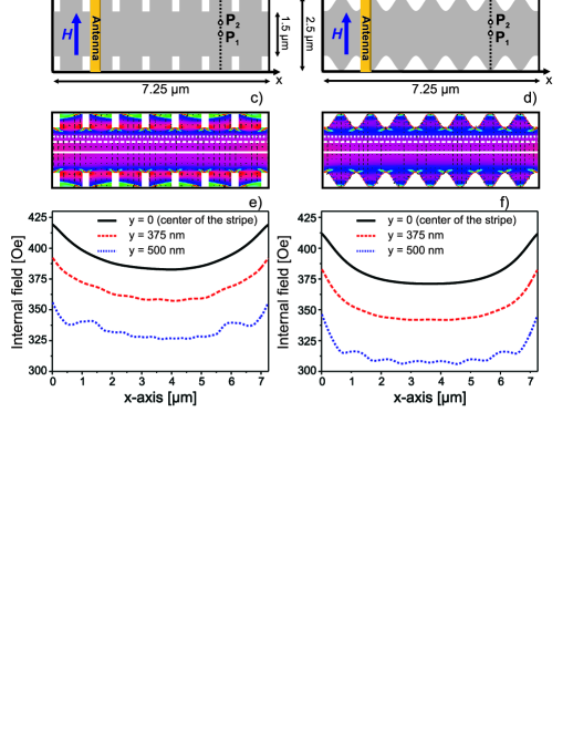
The two types of magnonic crystals under investigation are presented in Fig. 1a and Fig. 1b. They consist of 7.25 m-long Permalloy waveguides of 40 nm thickness. The width of both MCs varies between m and m with a period m. The geometry was chosen in such a way that the structure with rectangular notches is similar to the MC studied experimentally in Ref. [16]. The standard material parameters of Py used to simulate the dynamics of the magnetization are: saturation magnetization T, exchange stiffness constant J/m, and the magnetocrystalline anisotropy is assumed to be zero. The damping constant in the Landau-Lifshitz-Gilbert equation is considered to be . In order to avoid spin-wave reflection at the ends of the structure ( and m) the damping boundary conditions were used: In the boundary areas (m on each side) the parameter gradually increases more than fifty times resulting in a strong decay of the spin-wave intensity towards the boundaries.
In order to excite spin waves within a wide frequency range we apply a 70 ps-long video pulse to a 300 nm wide microstrip antenna (see Fig. 1). In this case the upper frequency limit given by the pulse duration is 13.5 GHz while the antenna can excite spin-waves with wavenumbers up to rad/m. The static biasing magnetic field of 500 Oe is applied in the film plane transverse to its long axis in order to satisfy the conditions for the excitation and propagation of the magnetostatic surface spin waves (MSSWs). These waves are known to have the highest values of the group velocity in magnetic microstructures and ensure spin-wave free paths of the order of several microns in Py.
For the understanding of the spin-wave excitation spectra in the magnonic crystals one need to take into account the distribution of the internal field shown in Fig. 1c and Fig. 1d for both MCs configurations. One can see that the magnetic field is non-uniform along both the long and short axis of the crystals. The field variation along the waveguides is not of crucial importance since it changes mostly near the ends of the waveguides (see the longitudinal field profiles along shown in Fig. 1e and Fig. 1f) where the spin-wave damping is artificially increased and no spin-wave propagation occurs. In contrast, the transverse field variation is of high importance: Even a small deviation from the longitudinal axis of m results in a shift in the field of about 30 Oe. This means that the internal field creates a spin-wave propagation channel in the middle of the waveguide [22]. As is visible in the figure the magnetic field is practically not modulated along this channel and the spin wave propagates in a non-periodic potential. Nevertheless, one can see that the bias field oscillates closer to the lateral edges of the waveguide (see dotted curves in Fig. 1e-f). This can be considered as a periodic variation of the effective width of the spin-wave channel.
In Fig. 2a the solid line represents the spin-wave transmission characteristics extracted from the simulated data for the notched MC. It was obtained by integrating the spin-wave intensity along the line drawn across the crystal at m away from the antenna (see dotted line in Fig. 1a). As it is expected no spin-wave transmission is allowed below the ferromagnetic resonance (FMR) frequency GHz as well as above the excitation cut-off frequency GHz.
The spin-wave band gap corresponding to the first Bragg wavenumber rad/m is visible at GHz. The second band gap ( rad/m) and the third one ( rad/m) are not as pronounced but are also clearly visible around 10.2 GHz and 11.9 GHz, respectively. The experimentally measured transmission characteristics [16] for the same magnonic crystal is shown in Fig. 2a with a dashed line. One can see that the first band gap is pronounced and has practically the same frequency as in the simulated data [23]. The higher-order rejection bands are not visible in the experiment due to limitation of the wavenumbers that can be excited by the m-wide antenna: rad/cm (note that in the simulations we use a 300 nm-wide antenna). Nevertheless, the results of the simulations are in good agreement with the experimental ones. Thus, our approach is trustworthy and can be used for further studies of MCs properties and characteristics.
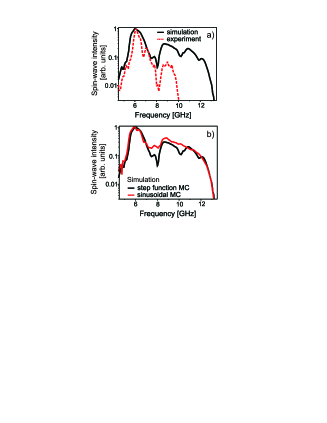
The comparison of the simulated transmission characteristics extracted from both notched and sinusoidal magnonic crystals is shown in Fig. 2b. One sees that the first band gap is visible for both structures and has exactly the same frequency. However, the second and the third band gaps do not exist for the sinusoidal magnonic crystal in contrast to the notched structure. This brings us to an important conclusion: The MCs transmission characteristics can be changed qualitatively by designing the MCs geometry. In addition, one can see that the first band gap is not so pronounced for the sinusoidal structure. This is in a good agreement with the results obtained in Ref. [16], where it has been shown that approximately half of the incident wave energy is reflected back from the notches due to the geometrical mismatch between the waveguide sections. In the case of a sinusoidal magnonic crystal this reflection vanishes which results in a smaller reflection parameter and a weaker rejection efficiency, respectively.
In general, several scattering mechanisms can contribute to the formation of the band gaps in the in-plane shaped magnonic crystals: (1) the reflection caused by the variation of the transverse spin-wave wavenumber (this wavenumber is inverse to the effective width of the spin-wave waveguide determined by the parameters of the spin-wave propagation channel) [16], (2) the scattering connected with the transformation of the spin-wave wavevector in the non-uniform internal magnetic field [24], and (3) the spin-wave reflection from the notches due to the geometrical mismatch (this mechanism is pronounced only for the notched MC).
Since in our case there is a relatively smooth internal field distribution inside of the spin-wave channel, the first mechanism appears to be dominant. We have estimated its role in the formation of the multiple rejection bands. In the approach of the uniform internal field, we can express the variation of the width in terms of wavenumbers as follows: The total wavevector of the propagating wave is given by: , in which represents the longitudinal wavevector, and are the transverse quantized wavenumbers due to the finite width () and finite thickness (), respectively. The integer parameters and represent the width and the thickness mode numbers. In our case is due to the small Py thickness and the uniform distribution of the dynamic magnetization on the film thickness. Moreover, becomes a function of the coordinate along the structure, and for sinusoidal and step function modulation we will have the corresponding relations:
| (1) |
| (2) |
where is the modulation amplitude, is the spatial coordinate along the structure, is the period of the modulation, and is the number of space harmonics in the Fourier series. The term represents the higher space harmonics of the parameter with amplitudes orders smaller than the first term. One can observe that both equations predict multiple rejection bands. However, the amplitudes given by the higher order terms are negligible in comparison with the ones given by the first term. This analytical prediction has been successfully proved by performing an additional simulation in which we considered a sinusoidally shaped waveguide with the maximal width variation of 0.75 m ( increase in the modulation depth in comparison with the previously shown data). The simulation has shown a single band gap in the spin-wave transmission characteristics.
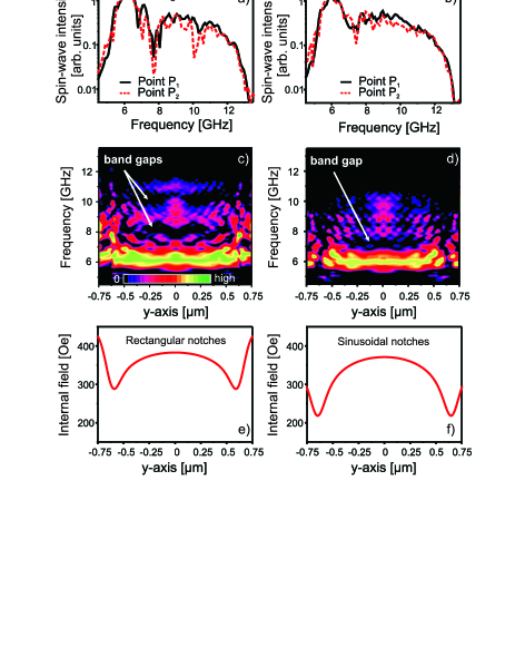
A deeper analysis reveals the dependence of the frequency and the depth of the rejection bands on the distance from the excitation antenna. It has been found that the band gaps appear already after the spin wave has passed two structural periods of the magnonic crystal. Furthermore, the simulation data shows that the rejection band depth depends also on the probing position across the MCs width. Figures 3a and 3b present the transmission characteristics extracted in two points: in the center of the structure (see Fig. 1a), and at half the distance between the center and the edge of the spin-wave propagation channel ( nm). One may note that the depth of the rejection bands is increased for both simulated structures. The dependence of the magnitude of the precessing magnetization component (or spin-wave amplitude) as a function of the position across the MC structures are shown in Fig. 3c and Fig. 3d. Several features are clearly visible: (1) the band gaps are more pronounced in the regions close to the edges of the waveguide rather than in the center, (2) the band gap frequency is slightly varied with the position, and (3) the absence of the rejection bands just near the waveguide edges. To understand the first feature one should consider that besides the modulation of the transversal wavevector, there is still a variation of the internal field. This variation is more pronounced closer to the notches than in the center of the magnonic crystal. Therefore, the spin wave which propagates close to the MCs edge is more sensitive to the modulation of the internal field which results in an increase of the rejection efficiency and a more pronounced band gap. The second feature is related to the decrease of the internal field towards the notches (see Fig. 3e and 3f). The change of the internal field produces a shift of the spin-wave dispersion characteristics triggering the shift of the band gap frequency. Moreover, the temporal evolution of the spatial distribution of the magnetization shows a complicated behavior at the edge of the structure. Standing waves formed inside the anti-notches are mixed with secondary higher-order width modes generated due to the scattering of the originally excited one at the edges [14]. As a consequence, the band gaps are vanishing at the edges of the spin-wave propagation channel (the third feature).
In conclusion, we performed a micromagnetic study of the spin-wave transmission in in-plane shaped microstructured magnonic crystals. Two kinds of spin-wave Permalloy waveguides magnetized across their longitudinal axes were investigated: with notched and sinusoidal edge profiles. In both cases spin waves propagate through a magnetically induced channel of varying effective width. It has been found that the waveguide width variation leads to the modulation of the spin-wave wavevectors, and consequently to the formation of frequency rejection bands in the spin-wave transmission characteristics. Both the band gap frequency and its depth depend strongly on the probing position inside the magnonic crystal due the non-uniform distribution of the internal magnetic field. The band gap properties including their number can be predefined by a proper choice of the magnonic crystal geometry.
Financial support by the DFG SE-1771/1-2 is gratefully acknowledged.
References
References
- [1] Vysotskii S L, Nikitov S A and Filimonov Yu A 2005 J. Exp. Theor. Phys. 101 636
- [2] Chumak A V, Serga A A, Hillebrands B and Kostylev M P 2008 Appl. Phys. Lett. 93 022508
- [3] Chumak A V, Serga A A, Wolff S, Hillebrands B and Kostylev M P 2009 J. Appl. Phys. 105 083906
- [4] Krawczyk M and Puszkarski H 2008 Phys. Rev. B 77 054437
- [5] Chumak A V, Serga A A, Wolff S, Hillebrands B and Kostylev M P 2009 Appl. Phys. Lett. 94 172511
- [6] Ustinov A B, Grigoreva N Yu and Kalinikos B A 2009 JETP Lett. textbf88 31
- [7] Chumak A V, Neumann T, Serga A A, Hillebrands B and Kostylev M P 2009 J. Phys. D: Appl. Phys. 42 205005
- [8] Gubbiotti G, Tacchi S, Carlotti G, Singh N, Goolaup S, Adeyeye A O and Kostylev M P 2007 Appl. Phys. Lett. 90 092503
- [9] Kostylev M P, Schrader P, Stamps R L, Gubbiotti G, Carlotti G, Adeyeye A O, Goolaup S and Singh N 2008 Appl. Phys. Lett. 92 132504
- [10] Wang Z K, Zhang V L, Lim H S, Ng S C, Kuok M H, Jain S and Adeyeye A O 2009 Appl. Phys. Lett. 94 083112
- [11] Chumak A V, Tiberkevich V S, Karenowska A D, Serga A A, Gregg J F, Slavin A N and Hillebrands B 2010 Nat. Commun. 94 141
- [12] Dvornik M and Kruglyak V V 2011 Phys. Rev. B 84 140405
- [13] Lee K S, Han D S and Kim S K 2009 Phys. Rev. Lett. 102 127202
- [14] Kim S K, Lee K S and Han D S 2009 Appl. Phys. Lett. 95 082507
- [15] Kruglyak V V, Hicken R J, Kuchko A B and Gorobets V Y 2005 J. Appl. Phys. 98 014304
- [16] Chumak A V, Pirro P, Serga A A, Kostylev M P, Stamps R L, Schultheiss H, Vogt K, Hermsdoerfer S J, Laegel B, Beck P A and Hillebrands B 2009 Appl. Phys. Lett. 95 262508
- [17] Chi K H, Zhu Y, Mao R W, Nikitov S A, Gulyaev Y V and Tsai C S 2011 IEEE Trans. Magn. 47 3708
- [18] Gurevich A G and Melkov G A 1996 Magnetization Oscillations and Waves (New York: CRC Press)
- [19] Serga A A, Chumak A V and Hillebrands B 2010 J. Phys. D: Appl. Phys. 43 264002
- [20] Karenowska A D, Gregg J F, Tiberkevich V S, Slavin A N, Chumak A V, Serga A A and Hillebrands B 2012 Phys. Rev. Lett. 108 015505
- [21] The simulations were performed using the OOMMF open code: Donahue M J and Porter D G 1999 Report NISTIR 6376, National Institute of Standards and Technology, Gaithersburg MD
- [22] Demidov V E, Demokritov S O, Rott K, Krzysteczko P and Reiss G 2008 Appl. Phys. Lett. 92 232503
- [23] To note that the spin-wave intensity was recorded in the experiment after 8 structure periods while in the simulation after 4 periods. Hence, one may observe a difference in the depth and the width of the first rejection band between the experimental data and simulation, and also a slight shift in frequency.
- [24] Kostylev M P, Serga A A, Schneider T, Neumann T, Leven B, Hillebrands B and Stamps R L 2007 Phys. Rev. B 76 184419