Device modeling of superconductor transition edge sensors based on the two-fluid theory
Abstract
In order to support the design and study of sophisticated large scale transition edge sensor (TES) circuits, we use basic SPICE elements to develop device models for TESs based on the superfluid-normal fluid theory. In contrast to previous studies, our device model is not limited to small signal simulation, and it relies only on device parameters that have clear physical meaning and can be easily measured. We integrate the device models in design kits based on powerful EDA tools such as CADENCE and OrCAD, and use them for versatile simulations of TES circuits. Comparing our simulation results with published experimental data, we find good agreement which suggests that device models based on the two-fluid theory can be used to predict the behavior of TES circuits reliably and hence they are valuable for assisting the design of sophisticated TES circuits.
Index Terms:
transition edge sensor, device model, superfluid-normal fluid, SPICEI Introduction
The past two decades have witnessed the rapid development of the superconductor transition edge sensor technology [1, 2] and its successful application in a wide range of scientific and instrumental fields [3, 5, 6, 4, 7]. Most impressively, mid scale TES detector arrays with tens to hundreds of pixels have been fabricated and deployed in Astronomy telescopes [8, 9]. In the near future, it is expected that much larger scale TES detector arrays, potentially with thousands to tens of thousands of pixels, will become available [10].
A fully functional TES detector array is a complex superconductor circuit system because all TES sensors at the pixel level need auxiliary supporting circuits for device biasing and signal readout. As the scale of the detector array grows, more system level circuits such as multiplexers [13, 12, 11] become indispensable too. It quickly becomes overwhelming to design and integrate all the necessary devices and circuits when the system size becomes large, and this challenge can only be met by elaborate electronic design automation (EDA) tools specifically developed for TES circuits.
Unfortunately, sophisticated tools that can support the simulation and design of large scale TES circuits are unavailable presently. An important reason for this deficiency is the lack of reliable TES device models that can be integrated in existing EDA tools to predict the behavior of TES circuits accurately. Since TESs are highly nonlinear electrothermal devices, their behavior is complicated and their modeling is difficult. Most previous research is limited to small signal models [2] which cannot be used for important tasks such as determining the required dc biases and deriving the temperature sensitivity from easily measurable device parameters. Some studies try to model the temperature dependence of TES resistance using fitting functions such as the hyperbolic function [14], the error function [15], the Fermi function [16] and other expressions [17, 18]. Though convenient in producing resistance-temperature (R-T) curves matching experimental data measured under certain conditions that are often very different than the actual working conditions for the TES devices (see Section IV-A), these models are not based on sound physical considerations and their applicability is difficult to justify. More seriously, since TESs are highly nonlinear devices, their R-T dependence and electrical and thermal behavior are very sensitive to how the circuits are designed and biased, as well as how the system is operated and how the R-T curves are measured (see Section IV-A). The fitting function approach that models the TES resistance as a sole function of the device temperature cannot capture this critical dependence on TES device’s working conditions and hence it is fundamentally flawed.
With the long term goal of making highly capable and integrated EDA tools that can support the design and simulation of large scale TES circuits, in this work we develop device models for TESs based on the superfluid-normal fluid theory. We choose SPICE as the modeling tool and use only the most basic SPICE circuit elements in order to be able to integrate our device model in the widest possible variety of circuit simulators. With the two-fluid theory as the underlying physical mechanism, the device model has the advantage that it only relies on device parameters that have clear physical meaning and can be measured easily. After integrating the device models in design kits based on powerful EDA tools such as CADENCE [19] and OrCAD [20], we then use them to perform a variety of simulations of TES circuits and compare the results to published experimental data to test the validity and accuracy of the device models.
II Device physics
In this section, we elaborate on the device physics that our TES model is based on. Since the TES sensor is an electrothermal device, we divide our discussion into the electric and thermal properties of the TES device.
II-A Electric behavior
The functioning of a TES sensor relies on the sharp transition between the device’s superconducting and normal states which is a very complex process. There are two well known theories to describe the transition physics, the Skocpol-Beasley-Tinkham (SBT) model [21] based on the phase-slip events in type I superconductors and the Kosterlitz-Thouless-Berezinsky (KTB) model [22, 23] based on flux vortex creation and interaction in type II superconductors. Though all superconductors used to fabricate TES devices are of type I, some authors argue that in two-dimensional thin films the vortex model is applicable [24]. The question which theory should be used to build electronic models that can describe TES device’s behavior accurately, or whether either model is suitable for this purpose at all, can only be answered by comparing the predicted behavior with experimentally measured data.
In our work, we are interested in building a simple model that captures the most important elements of the device physics and thus can be easily used to simulate the behavior of the TES device with reasonably good accuracy. For this purpose, we consider a simplified two-fluid model [25] which has its root in the SBT theory. In this model, the sensor current is separated into a supercurrent and a normal current . The total current is then
| (1) |
and a voltage can appear across the TES device because of the normal current. According to the SBT theory, the supercurrent , where is the temperature-dependent critical current of the TES film, and is the ratio of the time averaged critical current in the phase slip lines to . The normal current can be associated with the voltage across the device by , where is the normal state resistance of the TES device, and (usually approximately equal to 1) is the ratio of the total resistance of the phase slip lines in the TES film to .
In the two-fluid theory, the temperature dependence of the device’s critical current plays an essential role. In our simplified device model, it is the underlying mechanism for the temperature dependence of the TES resistance. For simple BCS superconductors that behave in accordance with Ginzburg-Landau theory, we have
| (2) |
where is the supercurrent of the TES device at 0 temperature and is the temperature normalized to the device’s critical temperature. For a single layer uniform film, the critical current can be expressed as a function of the sample’s other parameters such as the heat capacity and normal resistance [25]. Since most TES devices consist of multi-layer films made of different metals and rely on the proximity effect arising from such a structure, we do not expect this relation to hold and the supercurrent is an independent parameter in our device model. Nonetheless, the supercurrent and its temperature dependence can be easily measured.
Summarizing the main elements in the simplified two-fluid model, we can express the TES device’s equivalent resistance as
| (3) |
where is the voltage across the device. The nonlinear resistance described in Eq. (3) is implemented in our device model with the critical temperature , supercurrent and normal resistance being independent device parameters. Though highly simplified, it focuses on the most important mechanism underlying the TES device and simulation results based on it are consistent with many conclusions derived from experimental data. Notice that we have assumed 0 applied magnetic field. The effect of magnetic fields, as well as other factors that can affect TES device’s behavior, will be considered in improved versions of the device model.
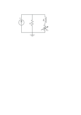
II-B Thermodynamics
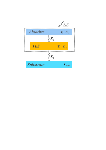
The thermal behavior of the TES device is dictated by the interplay of the Joule heating due to the device current and the heat conduction to the substrate. To describe the involved physics, we use a thermal model as shown in Fig. 1 which consists of an absorber, the TES device, and the substrate. This model is more comprehensive than most previous models which include only the TES and substrate. Notice that, if we assign a very large value to the absorber-TES heat conduction coefficient , the heat conduction between them is very efficient and they will remain at the same temperature. Therefore, the thermal model in Fig. 1 applies to devices without a dedicated absorber too.
We assume that heat conduction between the absorber, TES and substrate are governed by the power law
| (4) |
where is the power flow between two elements and , and are their temperatures, is the conduction coefficient, and is the exponent. Assuming the substrate temperature is fixed at , we can then write the thermal equation for the TES
| (5) |
where and are the temperatures of the TES and absorber, is the heat capacity of the TES, is the current through the TES, is the voltage across the TES, and , , and characterize the TES-substrate and absorber-TES heat conduction. In Eq. (5), the terms on the right hand side correspond to Joule heating and heat conduction to the substrate and from the absorber. Similar consideration leads to the thermal equation for the absorber
| (6) |
where is the heat capacity of the absorber and is the signal power.
Eqs. (5) and (6) are the basis of the thermal part of our device model which has , , , , and as its independent parameters. These device parameters have clear physical meaning. Their values depend on the materials and geometries of the device and can be measured by established experimental techniques. For simplicity, we have neglected the temperature dependence of these device parameters which should be weak in the temperature ranges that we are interested in.
III Modeling techniques
The two options available for TES device modeling are SPICE and analog HDL (hardware description language). In simulating and debugging TES circuits, we often need to examine signals on the internal nodes of the TES device. Behavior models built with analog HDL are less convenient for this purpose. Also, these models tend to be less efficient in circuit simulation, and their integration in SPICE and SPICE-like circuit simulators requires some effort. Because of these considerations, we choose SPICE as our modeling tool.
Though we have simplified the device physics as much as possible in section II, building SPICE models for the TES device is still quite involved. The main challenge lies in constructing equivalent electric circuit for the thermal part of the device model and modeling the nonlinear elements and processes in the device. Many latest circuit simulators have built-in nonlinear dependent source support. However, the syntax is simulator specific and the implementation details also vary. In order to be able to integrate our device model in the widest possible variety of circuit simulators, we choose to model the TES device using the polynomial controlled source which is supported in almost all circuit simulators.
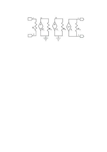
The polynomial controlled source [26] is a circuit element between two nodes whose voltage or current is dependent on one or more controlling signals. In the element description, the number of controlled signals, the nodes for the control signals, the polynomial coefficients, and the initial conditions for the controlling signals can be specified. For instance, a voltage-controlled voltage source Exx between the positive node N+ and negative node N- can be described as Exx N+ N- POLY(ND) (NC1+ NC1-) ... P0 P1 ... IC=..., where ND is the number of dimensions (i.e. the number of controlling signals), NC1+, NC1- ... are the positive and negative nodes of the controlling signals, P0, P1 ... are the polynomial coefficients, and the optional values following IC= specify the initial conditions for the controlling signals. Take as an example a two dimensional voltage source with controlling signals and , the controlled voltage is
| (7) |
Seemingly simplistic, the polynomial controlled source is extremely
powerful and can be used to realize many operations on multiple
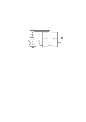
electric signals [27]. For example, the circuit
in Fig. 2(a) realizes the addition between two
voltages and with a polynomial controlled
source
E1 5 6 POLY(2) (1 2) (3 4) 0 1 1
To realize the multiplication between them,
use the polynomial controlled source
E1 5 6 POLY(2) (1 2) (3 4) 0 0 0 0 1
instead, as shown in Fig. 2(b) .
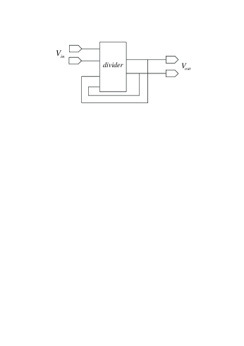
For division
between two voltages and , we use the circuit in
Fig. 2(c) where the two voltage controlled
current
sources
G1 0 10 POLY(1) (1 2) 0 1
and
G2 10 0 POLY(2) (3 4) (10 0) 0 0 0 0 1
play the central role. Since the currents in the two sources are
and in value, we
have . From this we can solve for the voltage across
nodes 10 and 0 which is
| (8) |
as long as the resistance is large. The voltage controlled voltage
source
E1 5 6 POLY(1) (10 0) 0 1
in parallel with the large resistance simply mirrors the
voltage so that the output voltage is the division
between the input voltages and .


In the following, we explain how the electric and thermal part of the TES physics and the coupling and feedback between them are modeled. We also describe relevant circuit diagrams.
III-A Electric behavior modeling
In order to model the voltage and temperature dependent TES resistance in Eq. (3),
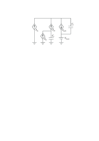
we use the circuits shown in Fig. 3. At the heart of
the circuit is the effective voltage controlled resistance in Fig.
3(a) realized by the following polynomial
voltage controlled current source
FIN 2 10 POLY(2) VIN VI 0 0 0 0 1
The current in this controlled current source FIN is
| (9) |
where and are
currents in the auxiliary 0 voltage sources VIN and VI. can
be calculated from the voltage of the voltage controlled voltage source
E1 20 0 POLY(1) (3 4) -1 1
and its value is ()
| (10) |
where is the voltage across nodes 3 and 4. Since the total current through the resistor Rx is
| (11) |
the voltage across nodes 1 and 2 is . The effective resistance between nodes 1 and 2 can then be calculated to be ()
| (12) |
Notice that the effective resistance across terminals 1 and 2 is
controlled by the voltage . If we design the circuit
appropriately so that is related to the voltage across
nodes 1 and 2 by the expression on the right hand side of Eq.
(3), we can then effectively realize a TES resistance
across these two nodes. This can be done by using the circuit in Fig.
3(b). This circuit has two inputs, the TES voltage
and another voltage equal to the TES supercurrent in value. The
TES voltage is scaled by the voltage controlled voltage source
E1 10 0 POLY(1) (1 2) 0 1/
and fed into the adder circuit which has as its other input.
The input signals to the divider circuit are the TES voltage and the
output from the adder circuit. The effective resistance across nodes
1 and 2 in Fig. 3(a) is then
| (13) |
where is the supercurrent and is the normal resistance of the TES device. The two-fluid theory based electric behavior of the TES device is then successfully modeled by our circuit.

III-B Thermodynamics modeling
SPICE is not designed to simulate thermodynamics. Though users can specify a temperature in circuit simulation, it is a constant ambient temperature used by device models to determine the electric characteristics of circuit elements (e.g. the diode current depends on not only its voltage bias but also the operation temperature). In order to study how the temperature of the TES device depends on its working condition, as well as how it changes in time, we must build equivalent electric circuit to simulate its thermodynamics.
As shown in Fig. 4(a) , the thermal equation (5) for the TES film can be mapped to the electric equation of a capacitor being charged by current sources whose values are given by the terms on the right hand side of the equation. The voltage across the capacitor corresponds to the temperature of the TES device, and the value of the capacitance is the heat capacity of the device. The current terms are dependent on the electric signals and temperature of the TES, thus they can be modeled by controlled polynomial sources.
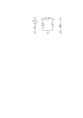

The circuit to model the Joule heating in equation
(5) is shown in Fig.
4(b) . In this circuit,
The voltage controlled voltage source
E1 20 0 POLY(1) (10 2) 0 1
simply duplicates the voltage across the resistor
Rx so that . The resistor
converts to a current
that is equal to in value:
| (14) |
Current in the current controlled polynomial current source
F1 3 4 POLY(2) V0 V1 0 0 0 0 1
is then
| (15) |
which is equal to the Joule heat in the resistor Rx. Using the TES device in place of Rx, we can then wire the controlled current source F1 in Fig. 4(a) to model the Joule heat dissipated by the TES device.
The heat conduction terms on the right hand side of Eq.
(5) can be directly modeled by controlled
polynomial sources. In Fig. 4(c),
the voltage controlled polynomial voltage sources
E1 10 0 POLY(1) (1 2) 0 0 0 0 0 1
and
E1 20 0 POLY(1) (3 4) 0 0 0 0 0 1
produce two voltages and , where
and represent temperatures of structures in the TES. The
polynomial controlled current source
G1 5 6 POLY(2) (10 0) (20 0) 0 K -K
then realizes a heat flow of . The heat
conduction exponent and in Eq. (5)
are material dependent and a value of 4 or 5 are often used. If
happens to be a non-integer (but rational) number, it can be written
as a fraction. From the numerator and denominator of the fraction,
we can construct appropriate power and root circuits using
polynomial controlled sources and realize the corresponding heat
flow.
Once we mapped the temperature of the TES to the voltage of a capacitor, and modeled the Joule heat of the TES and its heat flow to other parts of the system using polynomial controlled sources, we can then use the circuit in Fig. 4(a) to describe the thermal processes in the TES. The thermodynamics of the absorber in Eq. (6) can be modeled using the same techniques.
III-C Electrothermal coupling and feedback
The key to the operation of the TES device is the negative electrothermal feedback. When the temperature of the TES rises due to the absorption of signal power, the resistance of the device changes. This has the effect of changing the current and Joule power of the device and its heat flow to the substrate which in turn regulates the temperature of the device.
The effect of the TES resistance on the Joule power is already modeled in the thermal circuit in Fig. 4(b) where the equivalent current source for the Joule heat is realized by a polynomial current source controlled by the voltage and current of the TES. When the nonlinear resistance of the TES device changes, so does its Joule power.
The effect of the TES temperature on the device’s electric behavior
is manifested in the TES resistance in Eq. (3) where
the supercurrent changes with temperature. In order to model this
dependence, we use the circuit in Fig.
5(a). In this circuit, the input
voltage corresponds to the device
temperature , and the voltage controlled voltage sources
E1 10 0 POLY(1) (1 2) 1 -1/
and
E2 20 0 POLY(1) (10 0) 0 0 0
in combination with the square root circuit
X1 20 0 3 4 sqrt
produce an output signal
| (16) |
This is the temperature dependent supercurrent of the TES device, and it is fed into the circuit in Fig. 3(b) to model the TES resistance. The square root circuit is based on the divider circuit as shown in Fig. 5(b) where one of the input voltages to the divider circuit is set to the output. Since , we have .
Once we have designed circuits to model the electric and thermal behavior and the electrothermal feedback, we can construct a complete device model for the TES based on them. Notice that our TES device model is general purpose and can be used for important studies not supported by the small signal models developed in previous work.
IV Simulation based on the device model
Now that we have built the TES device model, we are interested in using it for simulation of TES circuits to test its validity. Considering the simplicity of the model and the large number of poorly understood and controlled factors in TES device fabrication, it is unrealistic to expect that simulation results based on our model will numerically agree with experimental data to exceedingly high precision for every fabricated TES device. However, a correct device model should give results that are consistent with important qualitative conclusions drawn from experimental data. By doing circuit simulation, we can also perform critical research on TES circuit design and operation. This includes important studies not possible before when only small signal models were available, such as determining the optimal bath temperature and electrical bias points for TES circuit operation and finding the allowed parameter margin space for TES device fabrication.
For the purpose of circuit simulation, we integrate the device model in popular EDA tools and leverage the power of these tools to carry out our studies. We use CADENCE and OrCAD which are based on UNIX and WINDOWS platforms respectively. The integration process mainly involves constructing subcircuits used in the device model, creating symbol views for them, and building a component library which contains the necessary subcircuits and the TES device model circuit itself. Once all subcircuits and components are created and tested, we can then use the graphic user interface (GUI) provided by the EDA tools to draw TES circuits, specify device parameters and run simulations. TES devices can be dragged into a circuit schematic and wired up to the rest of the circuit just like any other circuit elements such as resistors and inductors, and the EDA tools will automatically generate the circuit netlists, add the stimulus and device models and run the simulation using a simulator specified by the user. This greatly improves the efficiency of our research and reduces human error.
In the following, we describe some interesting TES circuit simulations we performed. We also analyze the results and check them against published experimental observations when possible.
IV-A Resistance-temperature (R-T) dependence
The width of the superconducting to normal transition is an important characteristic of the TES because the sharpness of the transition determines its temperature sensitivity. Some authors have tried to model the TES resistance using fitting functions that give the measured transition width and normal state resistance . Examples include the hyperbolic function (with the empirical parameter ) [14]
| (17) |
the error function [15]
| (18) |
as well as other mathematical expressions [16, 17, 18]. One notable problem with the fitting function approach is that the temperature sensitivity calculated from the derivative of the measured R-T curve is often much larger than that inferred from the device’s temporary response to a signal pulse. This is because the fitting function approach completely ignores the dependence of the R-T curve on the device’s working conditions which is often critical. We can study this issue using our device model.
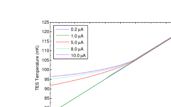
The circuit for a voltage biased TES device is shown in Fig. 6. The R-T curves are usually measured by biasing the TES sample with a constant near 0 current and sweeping the sample temperature. The reason to use a very small bias current is to minimize the Joule heat so that the TES sample remains at the same temperature with the substrate and environment. This temperature can be set and changed by the temperature controller of the refrigerator system, thus making it possible to measure the sample resistance at different temperatures. We can simulate this measurement process by a DC analysis based on our device model in which the environment temperature is the sweeping parameter. For this simulation, we need an exhaustive set of TES device parameters which is unfortunately not given in most published works. We use the data from reference [17] which is relatively complete. The result of the simulation is shown in Fig. 7(a). In order to check that the TES sample remains at the same temperature with the environment, the TES temperature is plotted against the environment temperature in Fig. 7(b). As can be seen from the figures, even though in the transition region the current biases are small enough to produce negligible Joule heat so that the TES sample remains at the same temperature with the environment, the transition width under each bias current can be quite different. Generally speaking, the smaller the bias current, the sharper the transition. This result clearly indicates that it is fundamentally flawed to model the TES resistance using fitting functions like those in Eqs. (17) and (18) without specifying the bias current under which the R-T curve is measured.
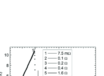
The working condition of the TES device is different than that for R-T curve measurement. The environment temperature is set below the device’s critical temperature, and a nonzero bias current is applied to bring the device’s temperature to within the transition region. To determine the device’s R-T dependence under this working condition, we perform a dc analysis in which is fixed and the circuit’s bias current in Fig. 6 is swept. The TES resistance is plotted against the device temperature in Fig. 8.
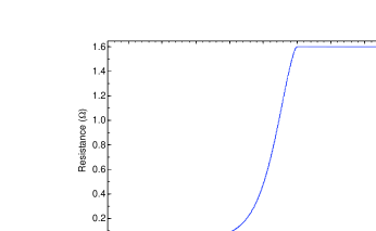
Comparing the results in Fig. 7 and Fig. 8, we notice that the transition width of a working TES device is much wider than that measured with near 0 bias current. While the transition width measured with near 0 current can be as low as sub mili Kelvin, the value for a working TES device is a few mili Kelvins. This explains why the TES device’s temperature sensitivity
| (19) |
( is the operation temperature of the TES and the resistance at ) calculated from the derivative of the measured R-T curve is usually much greater than that inferred from the device’s transient response to an input signal. The R-T dependence in Fig. 8 cannot be easily verified experimentally since the temperature of a working TES device cannot be measured directly, and our simulation allows to study it in detail. In setting the working condition for the TES device, it is nontrivial to determine values for the substrate temperature and bias current to optimize the device’s temperature sensitivity and other critical characteristics. Circuit simulations can help greatly in finding appropriate bias points and working conditions for the TES device. Otherwise, large number of measurements of the circuit’s IV characteristics must be performed.
IV-B Hysteresis in the temperature-bias current curve
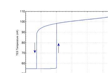
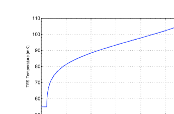
Another interesting phenomenon of the TES device is that it can display hysteresis when its temperature is adjusted with a bias current. In Fig. 6, when the bias current is increased, the temperature of the TES devices rises above the substrate temperature (i.e. the environment temperature) because of the Joule heating of the TES. Though the temperature - bias current curve cannot be directly measured (due to the difficulty in measuring the temperature of the TES), the characteristics of this curve have profound impact on the operation of the TES device and are therefore worth careful investigation. A DC analysis based on our device model can be used for this study.
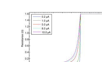
In Fig. 9, the simulated temperature - bias current curve of voltage biased TES device with different parameters are plotted. It can be seen that when the bias current is increased, the temperature of the TES does not increase with the bias current linearly. Instead, at some bias point it makes a sharp transition from a value close to the substrate temperature to a value close to the critical temperature of the device. More interestingly, for many device parameters, this sudden transition between near substrate temperature and near critical temperature can exhibit a hysteresis. After the TES temperature has made a sudden transition to close to the critical temperature at some bias current , if we subsequently decrease the bias current we can bring the device temperature back to close to the substrate temperature. This later temperature transition occurs suddenly too at some bias current , and can be different than giving rise to the hysteresis shown in Fig. 9(a).
The hysteresis in Fig. 9(a) is a consequence of the nonlinear nature of the TES device. Simulations show that for certain device parameter ranges the sudden temperature transition points can be very close to the critical temperature of the device and this can disrupt the normal operation of the TES and reduce its saturation input energy. In order to avoid such a scenario, care must be taken in the design phase to choose the device parameters correctly before it is fabricated. Such design work relies on large number of simulations of the circuit behavior and appropriate TES device models are indispensable.
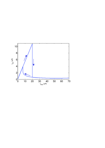
Though the temperature-bias current curve cannot be measured directly to observe the hysteresis in the device temperature, indirect experimental evidence is available. Some authors have measured the current in the TES branch against the total bias current in Fig. 6. The data can consist of a superconducting branch and a resistive branch as shown in Fig. 10(a) . When the bias current is decreased from the resistive branch, the TES eventually returns to the superconducting state, however the bias current at the transition point is different than that for the superconducting to resistive transition which leads to a hysteresis structure in Fig. 10(a). This is a manifestation of the hysteresis in the TES resistance, which in turn is due to the temperature hysteresis in Fig. 9(a). The current curve in Fig. 10(a) can be simulated using our device model and the result is plotted in Fig. 10(b) . The result agrees well with experimental data indicating the effectiveness of the device model.
IV-C Transient response to signal pulses
Our device model can be used directly in transient and AC analysis to simulate
temporal and frequency responses of the TES circuits to input signals. The
simulator will automatically linearize the circuit when necessary, saving the
trouble of manually deriving small signal models.
As an example, we simulate the transient response of the TES circuit in Fig. 6 to an input signal pulse under different circuit parameters. The TES temperature as a function of time is plotted in Fig. 11. Using the EDA tool’s parametric analysis functions, we can perform the same simulation for a range of circuit parameters in just one run and plot the results in the same figure. This makes it convenient to compare the results and observe how the response of the circuit changes with circuit parameters. In Fig. 11, we see that the circuit response becomes unstable when the inductance increases. This simple parametric simulation then allows us to determine the range of acceptable values of the inductance to ensure the stability of the response (when other circuit parameters are fixed). Such search for appropriate circuit parameter values is an important task in circuit design, and it is much more challenging when multiple parameters need to be considered simultaneously to maximize the circuit’s tolerance to fabrication errors. By developing sophisticated software that intelligently uses parametric simulations based on our device model in a multi-dimensional parameter space, it is possible to automate the critical task of optimizing circuit parameters [28].
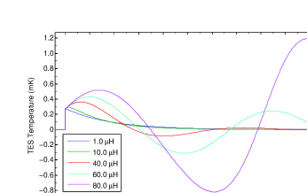
A direct comparison of the simulation results in Fig. 11 to experimental data is hindered by the incompleteness of the device parameters in reference [17]. However, the device’s temperature sensitivity suggested by the simulation appears to be smaller than the values given in the original reference for the same bias current. This indicates that our TES model based on idealized device physics might not give completely accurate numerical results for all TES devices considering the many uncertain and poorly controlled factors in the fabrication process that can impact the characteristics of the fabricated device. Of particular importance is the temperature dependence of the supercurrent in the superconducting to normal transition region since it determines the sharpness of the transition and hence the device’s temperature sensitivity. It is conjecturable that the exponent in the supercurrent - temperature relation can deviate from the BCS result in the transition region for practical devices, and simulation shows that the device’s temperature sensitivity is very sensitive to the value of . It is up to further theoretical and experimental studies to determine whether careful consideration of this issue can explain the discrepancy between the simulation and experimental data and lead to more accurate device models.
Though the example simulations we described in this paper are all based on the simple voltage biased TES circuit in Fig. 6, more sophisticated circuits can be simulated and more complex analysis can be performed using our device model. If we integrate the device model in a circuit simulator which supports Josephson devices such as WRspice [29], we will be able to simulate complete superconducting circuit systems that contain both TES devices and supporting Josephson circuits (e.g. SQUID amplifiers and multiplexers). Such powerful tool will make it possible to design and study large scale TES circuit systems for future scientific applications.
V Conclusion
In summary, we have developed a simple TES device model based on the superfluid - normal fluid theory. The device model is not limited to small signal simulations and can be used to study important characteristics of TES circuits and assist their design. Simulation results based on our device model are consistent with important observations and conclusions derived from experimental data, and they can be used to study phenomena not directly measurable in experiments. The device model can be improved by refining the device physics and considering neglected factors such as magnetic fields and noises. It is hoped that future improved device models will give better accuracy and reliability, so that they can be used to develop sophisticated EDA tools that can eventually support the design and simulation of large scale TES circuits.
References
- [1] A. J. Walton, W. Parkes, J. G. Terry, C. Dunare, J. T. M. Stevenson, A. M. Gundlach, G. C. Hilton, K. D. Irwin, J. N. Ullom, W. S. Holland, W. D. Duncan, M. D. Audley, P. A. R. Ade, R. V. Sudiwala, and E. Schulte, “Design and fabrication of the detector technology for SCUBA-2,” IEE Proc.-Sci. Meas. Technol., vol. 151(2), pp. 110 C120, 2004.
- [2] K. D. Irwin and G. C. Hilton, “Transition-edge sensors,” Topics Appl. Phys., vol. 99, pp. 63–152, 2005.
- [3] K. Irwin, G. Hilton, D. Wollman, and J. Martinis, “X-ray detection using a superconducting transition-edge sensor microcalorimeter with electrothermal feedback,” Appl. Phys. Lett., vol. 69, no. 13, pp. 1945–1947, 1996.
- [4] D. A. Wollman, S. W. Nam, D. E Newbury, G. C. Hilton, K. D. Irwin, N. F. Bergren, S. Deiker, D. A. Rudman, and J. M. Martinis, “Superconducting transition-edge-microcalorimeter x-ray spectrometer with 2eV energy resolution at 1.5 keV,” Nucl. Instr. Meth. A., vol. 444, pp. 145–150, 2000.
- [5] B. Cabrera, R. Clarke, A. Miller, S. W. Nam, R. Romani, T. Saab, and B. Young, “Cryogenic detectors based on superconducting transition-edge sensors for time-energy-resolved single-photon counters and for dark matter searches,” Physica B., vol. 280, pp. 509–514, 2000.
- [6] M. Krauss, and F. Wilczek, “Bolometric detection of neutrinos,” Phys. Rev. Lett., vol. 55, pp. 25–28, 1985.
- [7] K. Tanakaa, A. Odawara, S. Bandou, A. Nagata, S. Nakayama, K. Chinone, A. Yasaka, Y. Koike, S. Iijima, “Transition edge sensor system for material analysis using transmission electron microscope,” Physica C., vol. 469, pp. 881-885, 2009.
- [8] M. Ellis, “SCUBA-2 CCD-style imaging for the JCMT,” Exp. Astron., vol. 19, 169-174, 2005.
- [9] E. Shirokoff, B. A. Benson, L. E. Bleem, C. L. Chang, H-M. Cho, A-T. Crites, M. A. Dobbs, W. L. Holzapfel, T. Lanting, A. T. Lee, M. Lueker, J. Mehl, T. Plagge, H. G. Spieler, and J. D. Vieira, “The south pole telescope SZ-receiver detectors,” IEEE Trans. Appl. Supercond., vol. 19, no. 3, pp. 517–519, 2009.
- [10] W. Holland, “SCUBA-2: A 10 000 pixel submillimeter camera for the james clerk maxwell telescope,” Proc. SPIE., vol. 6275, pp. 62751E, 2006.
- [11] J. Chervenak, K. Irwin, E. Grossman, J. Martinis, C. Reintsema, and M. Huber, “Superconducting multiplexer for arrays of transition edge sensors,” Appl. Phys. Lett., vol. 74, no. 26, pp. 4043–4045 , 1999.
- [12] K. D. Irwin, “SQUID multiplexers for transition-edge sensors,” Physica C., vol. 368, pp. 203–210, 2002.
- [13] D. J. Benford, G. M. Voellmer, J. A. Chervenak, K. D. Irwin, S. H. Moseley, R. A. Shafer, G. J. Stacey, and J. G. Staguhn, J. Wolf, J. Farhoomand, and C. R. McCreight, “Thousand-element multiplexed superconducting bolometer arrays,” Proc. Far-IR, Sub-MM, and MM Detector Workshop., vol. NASA/CP-2003-211 408, pp. 272–275, 2003.
- [14] J. A. Burney, Transition-edge sensor imaging arrays for astrophysics applications, PhD thesis, Stanford University, 2007.
- [15] A. J. Miller, Development of a Broadband Optical Spectrophotometer Using Superconducting Transition-Edge Sensors, PhD thesis, Stanford University, 2001.
- [16] M. Ukibe, M. Koyanagi, M. Ohkubo, H. Pressler and N. Kobayashi, “Characteristics of Ti flims for transition edge sensor microcalorimeters,” Nucl. Instr. and Meth. A, vol. 436 pp. 256–261, 1999.
- [17] E. Taralli, C. Portesi, R. Rocci, M. Rajteri and E. Monticone, “Investigation of Ti/Pd bilayer for single photon detection,” IEEE Trans. Appl. Supercond., vol. 19, no. 3, pp.493–495, 2009.
- [18] P. Roth, G. W. Fraser, A. D. Holland, and S. Trowell, “Modelling the electro-thermal response of superconducting transition-edge x-ray sensors,” Nucl. Instrum. Meth. A., vol. 443, pp. 351–363, 2000.
- [19] http://www.cadence.com/products/cic/Pages/default.aspx
- [20] http://www.cadence.com/products/orcad/pages/default.aspx
- [21] W. J. Skocpol, M. R. Beasley, and M. Tinkham, “Phase-slip centers and nonequilibrium processes in superconducting tin microbridges,” J. Low Temp. Phys., vol. 16, pp. 145–167, 1974.
- [22] V. L. Berezinskii, “Destruction of Long-range Order in One-dimensional and Two-dimensional Systems Possessing a Continuous Symmetry Group. II. Quantum Systems,” Sov.Phys. JETP., vol. 34, pp. 610–616, 1972.
- [23] J. M. Kosterlitz and D. J. Thouless, “Ordering, metastability and phase transitions in two-dimensional systems,” J. Physics. C: Solid State Physics., vol. 6, pp. 1181–1203, 1973.
- [24] G. W. Fraser, “On the nature of the superconducting-to-normal transition in transition edge sensors,” Nucl. Instrum. Meth. A., vol. 523, pp. 234–245, 2004.
- [25] K. D. Irwin, G. C. Hilton, D. A. Wollman, and J. M. Martinis, “Thermal-response time of superconducting transition-edge microcalorimeters,” J. Appl. Phys., vol. 83, pp. 3978–3985, 1998.
- [26] http://newton.ex.ac.uk/teaching/cdhw/Electronics2/userguide/secC.html
- [27] Ron M. Kielkowski, SPICE: Practical Device Modeling, McGraw-Hill,1995.
- [28] C. J. Fourie and W. J. Perold, “Comparison of genetic algorithms to other optimization techniques for raising circuit yield in superconducting digital circuits,” IEEE Trans. Appl. Supercond., vol. 13, no. 2, pp. 511–514, 2003. Q. P. Herr and M. J. Feldman, “Multiparameter optimization of RSFQ circuits using the method of inscribed hyperspheres,” IEEE Trans. Appl. Supercond., vol. 5, no. 2, pp. 3337–3340, 1995.
- [29] http://www.wrcad.com/wrspice.html