Crossover from Coulomb blockade to quantum Hall effect in suspended graphene nanoribbons
Abstract
Suspended graphene nano-ribbons formed during current annealing of suspended graphene flakes have been investigated experimentally. Transport measurements show the opening of a transport gap around charge neutrality due to the formation of ”Coulomb islands”, coexisting with quantum Hall conductance plateaus appearing at moderate values of magnetic field . Upon increasing , the transport gap is rapidly suppressed, and is taken over by a much larger energy gap due to electronic correlations. Our observations show that suspended nano-ribbons allow the investigation of phenomena that could not so far be accessed in ribbons on SiO2 substrates.
pacs:
72.80.Vp,73.43.Qt,73.23.Hk,85.35.-pTheoretical studies indicate that in graphene nano-ribbons (GNRs) –long and narrow graphene channels– Dirac electrons should give origin to a number of unique phenomena, accessible in transport experiments. Examples include the controlled opening of a band gap Nakada96 , the realization of gate-tunable magnetic states Son06 , or the interplay between Landau and size quantization Peres06 . Theories, however, usually consider disorder-free GNRs with idealized edge structure Nakada96 ; Son06 ; Peres06 , whereas disorder is invariably present in experimental systems, which leads to the formation of localized states in a wide energy range Han07 ; Moliter09 ; Oostinga10 . In the presence of strong disorder, transport through GNRs near charge neutrality is mediated by hopping, and GNRs behave as an ensemble of randomly assembled quantum dots, resulting in the opening of a so-called transport gap Han07 ; Moliter09 ; Oostinga10 . In this regime, even the most basic manifestations of the Dirac character of electrons, such as the half-integer conductance quantization in a magnetic field Novoselov05 , are washed out Moliter09 ; Oostinga10 .
A complete elimination of disorder would require control of the edge structure Poumirol10 ; Jiao11 , and the fabrication of suspended GNR devices to avoid the influence of substrate-induced disorder Du08 . The high electronic quality of suspended graphene devices has indeed been demonstrated –among others– by the observation of ballistic transport Du08 ; Tombros11 and of the fractional quantum Hall effect in monolayers Du09 ; Bolotin09 , and of small interaction induced gaps in bilayers Weitz10 . Crucial to achieve high-quality is a current annealing step, i.e., forcing a large current to heat graphene, in order to desorb adsorbates from the surface Du08 ; Moser07 . The large current required can lead to cleavage of graphene, which usually results in device failure. We have found that in several cases a partial graphene cleavage can occur Tombros11 ; Moser09 , leading to the formation of narrow suspended nano-ribbons.
Here, we report on magneto-transport measurements through a device produced in this way. We find that, while a disorder-induced transport gap still opens around charge neutrality (as observed in lithographically defined GNRs on SiO2 substrates Han07 ; Moliter09 ; Oostinga10 ), Coulomb blockade is strongly suppressed by the application of only a moderate magnetic field ( T) Oostinga10 ; Poumirol10 . This leads to quantum Hall conductance plateaus at finite carrier density, and the occurrence of a strongly insulating state (with a gap increasing with magnetic field) around charge neutrality Checkelsky08 . These phenomena, normally observed only in sufficiently clean graphene Du08 ; Tombros11 ; Du09 ; Bolotin09 , indicate that suspension of GNRs result in a significant improvement of their electronic quality, enabling the observation of phenomena not accessible in GNRs on SiO2 substrates Han07 ; Moliter09 ; Oostinga10 ; Poumirol10 .
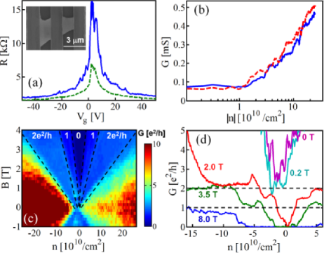
Wide suspended graphene devices are fabricated using polydimethylglutarimide (PMGI) resist (LOR, MicroChem) as a sacrificial supporting layer, as described by Tombros et al. (see Ref. 18 for details). Measurements are performed in a two-terminal configuration with Ti/Au contacts (10/70 nm) separated by a distance of approximately 0.5-1 m (depending on the device), using the highly doped Si substrate as gate electrode (approximately 1 m away from graphene). The inset in Fig. 1(a) shows a scanning electron microscope (SEM) image of a successfully annealed device.
Current annealing was performed by slowly ramping up the bias voltage to -2 V (depending on the specific sample) in vacuum at 4.2 K, and maintaining the applied bias for extended periods of time. For most devices, this procedure had to be repeated several times before a sharp resistance peak at approximately zero gate voltage ( V) could be observed (see Figs. 1(a),(b)). In successfully annealed devices, low-field integer quantum Hall effect with a complete lifting of spin and valley degeneracy was observed, together with a strongly insulating state appearing at charge neutrality upon the application of a magnetic field (see Figs. 1(c),(d)). These observations and the narrow width of the resistance peak around charge neutrality ( cm-2) indicate the high device quality Du08 ; Tombros11 ; Du09 ; Bolotin09 .
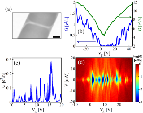
In several different devices, we observed sudden, large increases in resistance during annealing, originating from partial breaking of the graphene layer (see, e.g., Fig. 2(a)). In these cases, the measured dependence of the conductance exhibits features that are characteristically observed in nano-ribbons Han07 ; Moliter09 ; Oostinga10 . Figs. 2(b)-(d) show data from a device in which the phenomenon was seen more clearly. Specifically Fig. 2(b) shows the dependence of the conductance before (green curve) and after (blue curve) a final annealing step, which resulted in the opening of a transport gap in the range between 0 and 20 V. In this range, a random sequence of conductance peaks is observed (Fig. 2(c)), and measurements of the differential conductance versus and show ”Coulomb diamonds” characteristic of a disordered array of quantum dots (Fig. 2(d)). This is the same behavior observed in GNRs on SiO2 substrates Han07 ; Moliter09 ; Oostinga10 .
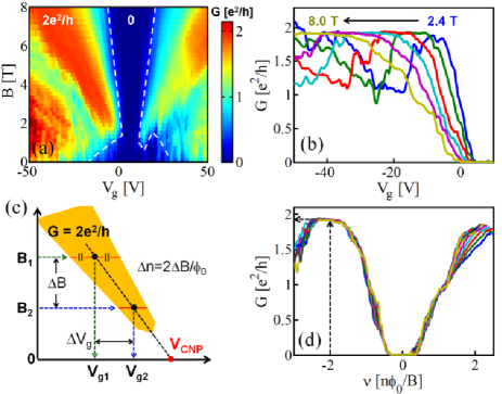
Measurements as a function of illustrate the difference between suspended GNRs and GNRs on SiO2 Moliter09 ; Oostinga10 ; Poumirol10 . Fig. 3(a) shows the and dependence of the conductance, where quantum Hall states with are observed for holes and for electrons. The quantization of the conductance is better seen in Fig. 3(b), which shows cuts at fixed of the color plot in Fig. 3(a). For negative , the plateaus appear at T, whose conductance is very close to 2 (; the deviation is due to a 350 contact resistance) as expected for Dirac electrons Novoselov05 . For positive gate voltages, the plateaus become well defined only at larger magnetic field (see Fig. 3(d)) note1 . Around charge neutrality and for T, a strongly insulating state is seen, similarly to what is normally observed in large, clean suspended graphene flakes Du09 ; Bolotin09 , originating from interaction-induced electronic correlations Checkelsky08 .
To further test the quantum Hall nature of the plateaus we plot the conductance as a function of filling factor (with and carrier density), to check if all data collapse on a single curve as expected. To extract the carrier density as a function of , we exploit the fact that at the center of a 2 conductance plateau at a fixed magnetic field , (owing to spin degeneracy) so that . We then find that the carrier density scales linearly with gate voltage, as it should. The slope cm-2V-1 is slightly larger than the value, 4.7 cm-2V-1, estimated from the formula for a parallel plate capacitor, as expected, since the ribbon width note1 is smaller than the distance to the gate (the value of agrees quantitatively with a recent study of suspended graphene in the quantum Hall regime Marun11 , where an enhanced capacitance at the edges was found). By extrapolating to T, we find that charge neutrality occurs at V (see Fig. 3(c)). Using this relation between and , we plot the conductance as a function of in the range between 5.0 and 8.0 T (Fig. 3(d)). On the hole side all curves collapse together nearly perfectly; on the electron side the trend is similar, and although the collapse is not as good, the presence of a 2 quantum Hall plateau becomes apparent.
We conclude that in suspended GNRs the transport gap due to Coulomb islands at T coexists, at T, with quantum Hall effect at finite carrier density, and with a large-gap correlated state around charge neutrality. As these phenomena occur at low magnetic field only when the level of disorder is sufficiently low Du08 ; Tombros11 ; Du09 ; Bolotin09 , their observation indicates that the quality of suspended GNRs created during current annealing is considerably better than that of GNRs on SiO2 substrates Han07 ; Moliter09 ; Oostinga10 ; Ribeiro11 . Similarly to larger suspended graphene devices, the low disorder level in suspended GNRs is due to the absence of a substrate and to the current annealing. The current-induced cleaving process –which occurs in vacuum– may also lead to better edges Jia09 as compared to lithographically defined GNRs Han07 ; Moliter09 ; Oostinga10 .
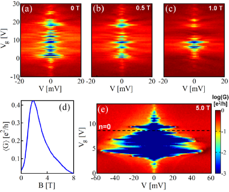
The higher quality enables the investigation of the competition between Coulomb blockade –originating from geometrical confinement in the presence of disorder– and the quantum-Hall effect, due to magnetic confinement. One interesting aspect is the dependence of the transport gap on magnetic field. Fig. 3(a) shows that the transport gap due to Coulomb islands (i.e., the interval where the conductance is strongly suppressed) narrows down with increasing from 0 to 1 T. The phenomenon is illustrated in more detail in Figs. 4(a)-(c), which show measurements of Coulomb diamonds for different values of . While at T diamonds appear when is between 0 and V, at T they are only present between and 10 V. Correspondingly, the conductance averaged over between 0 V and 20 V increases by more than ten times as is increased from 0 to T (Fig. 4(d)). An increase in the averaged conductance was found previously in GNRs on SiO2 substrates Oostinga10 ; Poumirol10 , and correctly attributed to a magnetic-field induced increase of the electron localization length, but a full crossover from a Coulomb blockaded regime to fully developed conductance quantization has not been observed previously Moliter09 ; Oostinga10 ; Poumirol10 ; Ribeiro11 .
Note that, at low carrier density, a large increase in the two-terminal conductance of a narrow disordered wire (i.e. where at T electron states are localized) upon entering the quantum Hall regime is a manifestation of the Dirac fermion character of the charge carriers. If electrons were described by the Schrodinger equation –as it would be the case for a narrow wire defined in a conventional two-dimensional electron gas– entering the quantum Hall regime at low carrier density would result in a so-called sub-band depopulation (due to the enhanced magnetic field confinement), and in a decrease of the two terminal conductance with increasing Beenakker91 . For Dirac electrons, the existence of a zero-energy Landau level is responsible for this difference, and causes the conductance to increase.
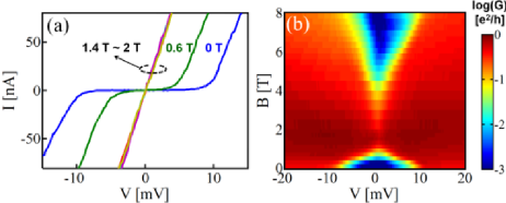
The crossover from the Coulomb-blockaded regime at T –characterized by non-Ohmic curves– to a linear transport regime at finite magnetic field (see Fig. 5(a)) is also apparent in measurements at fixed in the ”transport gap” range. Fig. 5(b) shows data taken at V, in which a 10 meV gap due to charging energy at T closes when is increased to 1.4 T (at T, decreases again due to the large gap associated to the correlated state around the charge neutrality point). The full suppression of Coulomb blockade is expected in GNRs exhibiting a clear quantum-Hall effect, since plateaus with quantized conductance (Fig. 3) indicate that transport is mediated by edge states and that backscattering is absent. This implies that electrons are delocalized over the full device length, so that transport is not any more blocked by the Coulomb charging energy associated to localized states in ”disorder-induced islands”.
Finally, we discuss the crossover –at charge neutrality– between the transport gap due to Coulomb islands, and the gap at large values. The transport gap associated to Coulomb islands is not a ”true” gap in the density of states, i.e. states are still present at low energy. On the contrary, the strongly insulating state appearing for T seems to have a true gap, since no current can be detected at low bias over a large range (Fig. 4(e)). Contrary to the transport gap associated to Coulomb blockade, this gap increases with increasing (see Fig. 3(a) and Fig. 5(b)) and at sufficiently large , it behaves virtually identically to what is found in clean suspended layers of larger width (see Fig. 2(c)) Du09 ; Bolotin09 . Note that, as observed in Ref. 13, the correlation induced gap in Fig. 4(e) is asymmetric around the charge neutrality point, i.e., electron-hole symmetry is broken in the underlying electronic state .
We conclude by comparing our results to those of Ref. 11, where Tombros et al. realized a constriction by annealing a suspended graphene flake, and observed signatures of conductance quantization (i.e. ballistic transport) at T, whereas at T we observe carrier localization. What appears to be mainly responsible for the different behavior is the device length. In Ref. 11 the length of the constriction is comparable to (or shorter than) the width; in all devices imaged by us, the length of the structures is much longer than their width. Edge scattering is therefore much more severe, resulting in electron localization and preventing ballistic transport. It is clear that systematic investigations of suspended devices as a function of their width and length are worth pursuing, to explore the properties of confined Dirac electrons in different transport regimes. Such a study would provide information on the mechanisms of edge scattering and on the nature of edge disorder, two virtually unexplored aspects of graphene nano-structures. A difficulty is the lack of control of the dimensions of the structures that are created by current annealing, and it will be crucial to make the fabrication process more controllable (e.g., by ”seeding” structural defects in the graphene layer before suspension, where annealing-induced cleavage occurs preferentially). Even without this control, our results show that nano-ribbons generated by annealing suspended graphene enable the observation of new and interesting phenomena.
We acknowledges N. Tombros for discussions about device fabrication and A. Ferreira for technical support. Financial support from the NCCRs MANEP, and QSIT, and from SNF is gratefully acknowledged.
References
- (1) K. Nakada, M. Fujita, G. Dresselhaus, and M. S. Dresselhaus, Phys. Rev. B 54, 17954 (1996); L. Brey and H. A. Fertig, Phys. Rev. B 73, 235411 (2006); Y. W. Son, M. L. Cohen, and S. G. Louie, Phys. Rev. Lett. 97, 216803 (2006).
- (2) Y. W. Son, M. L. Cohen, and S. G. Louie, Nature 444, 347 (2006); O. V. Yazyev, Rep. Prog. Phys. 73, 056501 (2010).
- (3) N. M. R. Peres, A. H. Castro Neto, and F. Guinea, Phys. Rev. B 73, 241403(R) (2006); A. A. Shylau, I. V. Zozoulenko, H. Xu, and T. Heinzel, Phys. Rev. B 82, 121410(R) (2010); A. A. Shylau and I. V. Zozoulenko, Phys. Rev. B 84, 075407 (2011).
- (4) M. Y. Han, B. Özyilmaz, Y. Zhang, and P. Kim, Phys. Rev. Lett. 98, 206805 (2007); C. Stampfer et al., Phys. Rev. Lett. 102, 056403 (2009); M. Y. Han, J. C. Brant, and P. Kim, Phys. Rev. Lett. 104, 056801 (2010); P. Gallagher, K. Todd, and D. Goldhaber-Gordon, Phys. Rev. B 81, 115409 (2010); S. Dröscher, H. Knowles, Y. Meir, K. Ensslin, and T. Ihn, Phys. Rev. B 84, 073405 (2011).
- (5) F. Molitor et al., Phys. Rev. B 79, 075426 (2009); S. Schmidmeier et al., arXiv:1111.4330 (unpublished).
- (6) J. B. Oostinga, B. Sacépé, M. F. Craciun, and A. F. Morpurgo, Phys. Rev. B 81, 193408 (2010); J. Bai et al., Nature Nanotech. 5, 655 (2010).
- (7) K. S. Novoselov et al., Nature (London) 438, 197 (2005); Y. Zhang, Y. W. Tan, H. L. Stormer, and P. Kim, Nature (London) 438, 201 (2005).
- (8) J. M. Poumirol et al., Phys. Rev. B 82, 041413(R) (2010).
- (9) L. Jiao, X. Wang, G. Diankov, H. Wang, and H. Dai, Nature Nanotech. 5, 321 (2011); T. Shimizu et al., Nature Nanotech. 6, 45 (2011); X. Wang et al., Nature Nanotech. 6, 563 (2011); M. W. Lin et al., Phys. Rev. B 84, 125411 (2011); M. W. Lin et al., Nanotech. 22, 265201 (2011).
- (10) X. Du, I. Skachko, A. Barker, and E. Y. Andrei, Nature Nanotech. 3, 491 (2008); K. I. Bolotin et al., Solid State Commun. 146, 351 (2008).
- (11) N. Tombros et al., Nature Phys. 7, 697 (2011).
- (12) X. Du, I. Skachko, F. Duerr, A. Luican, and E. Y. Andrei, Nature (London) 462, 192 (2009)
- (13) K. I. Bolotin, F. Ghahari, M. D. Shulman, H. L. Stormer, and P. Kim, Nature (London) 462, 196 (2009).
- (14) R. T. Weitz, M. T. Allen, B. E. Feldman, J. Martin, and A. Yacoby, Science 330, 812 (2010); F. Freitag, J. Trbovic, M. Weiss, and C. Schönenberger, Phys. Rev. Lett. 108, 076602 (2012); J. Velasco Jr et al., Nature Nanotech. 7, 156 (2012); A. Veligura et al., arXiv:1202.1753 (unpublished).
- (15) J. Moser, A. Barreiro, and A. Bachtold, Appl. Phys. Lett. 91, 163513 (2007).
- (16) J. Moser and A. Bachtold, Appl. Phys. Lett. 95, 173506 (2009).
- (17) J. G. Checkelsky, L. Li, and N. P. Ong, Phys. Rev. Lett. 100, 206801 (2008); Phys. Rev. B 79, 115434 (2009); M. O. Goerbig, Rev. Mod. Phys. 83, 1193 (2011).
- (18) N. Tombros et al., J. Appl. Phys. 109, 093702 (2011).
- (19) It has not been possible to image all the nano-ribbons produced by annealing, because most devices broke in the course of the experiments, which gives an uncertainty about their dimensions. In the cases that we could image, the nano-ribbon length was comparable to the contact separation (see Fig. 2(a)). For the nano-ribbon whose data we show here the width can be estimated from the results of the measurements. Quantum Hall plateaus starting at 2-2.5 T indicates that nm, since otherwise the edge states at opposite edges would overlap, preventing the observation of conductance quantization. By comparing the charging energy ( 10 meV, see Fig. 2(d)) to data measured in ribbons on SiO2 –and given that the dielectric constant of SiO2 partially screens Coulomb interactions– we also estimate that nm.
- (20) I. J. Vera-Marun et al., arXiv:1112.5462 (unpublished).
- (21) R. Ribeiro et al. [Phys. Rev. Lett. 107, 086601 (2011)], observed 2 quantum-Hall conductance quantization in a GNR, but only at high field, in pulsed magnetic field experiments. In those experiments, no clear evidence of the correlation induced gap around charge neutrality was found even at T.
- (22) X. Jia et al., Science 323, 1701 (2009).
- (23) C. W. J. Beenakker and H. van Houten, Solid State Physics 44, 1 (1991).