R&D Status of FPCCD Vertex Detector for ILD
Abstract
Fine pixel CCD (FPCCD) is one of the candidate sensor technologies for the vertex detector used for experiments at the International Linear Collider (ILC). A vertex detector system for the International Large Detector (ILD) using FPCCD sensors has been designed. We report on the R&D status of FPCCD sensors, as well as the vertex detector design for ILD.
1 Introduction
Performance goal of vertex detectors for ILC experiment is not easy to accomplish. The requirement for the impact parameter resolution is better than m. The innermost layer should have tolerance against beam background of less than few % pixel occupancy and radiation immunity from electroncmy. Bunched beam of ILC could induce RF noise, which was a serious problem at SLD.
There are many sensor technology options proposed to meet these challenges. One possible solution for these issues is the fine pixel CCD (FPCCD) option [1]. FPCCD sensors will have the pixel size of m and will be read out in ms between bunch trains. Because there is no beam crossing during the readout, FPCCD sensor option is completely free from the RF noise. The present goals of the FPCCD sensor R&D are listed in Table 1.
Pixel size 6 m Chip size 1 cm 6.5 cm Readout speed Mpix/s Full well capacity electrons Power consumption mW/ch Radiation tolerance electron/cm2
In addition to the sensor R&D, we need a realistic design of the vertex detector which can be used for realistic simulation study of the performance of the detector system for the ILC experiment. In this report, we also discuss engineering R&D and a design of the vertex detector for ILD (International Large Detector) [2] which is one of the validated detector systems for ILC.
Our R&D activity also includes R&D of the readout ASIC for FPCCD sensors. It is however described elsewhere in these proceedings [3].
2 FPCCD sensor R&D
Just after the decision of the RF technology for the ILC main linac by the International Technology Recommendation Panel (ITRP) in 2004, we have started R&D on the FPCCD sensors in cooperation with Hamamatsu Photonics. We first developed fully depleted CCD sensors with a standard pixel size of 24 m. Because signal charge in a pixel should not spread over several pixels by diffusion in order to suppress the pixel occupancy, the fully depleted epitaxial layer is essential for the FPCCD sensors. After establishing the technology of fully-depleted CCD sensors [4], prototype FPCCD sensors have been manufactured 4 times. First 2 prototypes have 12 m pixels [5] and latter 2 prototypes have four different pixel sizes,12, 9.6, 8, and 6 m in one chip [6]. The size of the image area of these prototypes is about 6 mm square.
In the third prototype sensors, the 12, 9.6, and 8 m pixels worked properly, but the 6 m pixels did not work at all. In the latest prototype (the fourth prototype) sensors, the potential profile has been improved based on the device simulation. About a factor 2 improvement of the depth of the potential well is expected. By this improvement, some signal can be seen for the 6 m pixels in the 4th prototype, but the signal from the pixels far from the readout node is quite small, and we need still more improvement for the 6 m pixels.
The next prototype sensors have been designed and will be delivered in Japanese fiscal year of 2012. This prototype is the first large size ( cm cm) prototype. It has 8 sections and each section has the pixel size of 12, 8, or 6 m. Horizontal shift registers for 6 m pixels have a size of m m to improve the full-well capacity and to decrease resistance of the gate lines. There are multiple wires for gate lines and there are many bonding pads for these wires along the longer side of the chip.
3 Engineering R&D
3.1 Sensor thinning
It is crucial to minimize multiple scattering of charged particles by the sensors and the support structure (ladders) in order to achieve the excellent impact parameter resolution mentioned in section 1. Therefore very low material budget is required for the ladders of the vertex detector in ILC experiment. Our ultimate goal is the radiation length of 0.1%/layer.
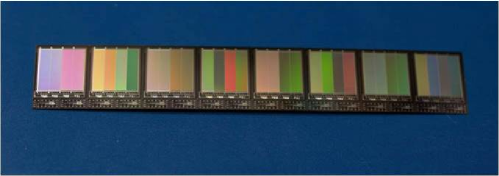
Sensor thinning is inevitable to achieve the ultra light ladder. Hamamatsu Photonics has fabricated sample sensors thinned down to 50 m. Figure 1 shows the prototype CCD sensor which has the size of 60 mm 9.7 mm50 m. The wafer was thinned by mechanical grinding after the processing and diced into chips. No increase of dark current was observed in these thinned chips. Such thin sensors cannot be completely flat. There are 0.3–0.7 mm sag over the length of 60 mm.
3.2 Two-phase CO2 cooling
FPCCD sensors will be operated at low temperature (C) inside a cryostat in order to minimize the effect of radiation damage, particularly minimize the charge transfer inefficiency (CTI). On the other hand, the expected power consumption inside the cryostat including sensors and readout ASICs is close to 100 W. If we try to cool this vertex detector with cold air or nitrogen gas, the flow rate will be quite large and could cause vibration of the ladders. We thus consider a cooling system using two-phase CO2.

The two-phase CO2 cooling system is a very attractive alternative because of its large cooling capacity of J/g. Cooling tube will be attached to the end plates of the vertex detector and the heat produced by CCD output amplifiers and readout ASICs will be removed by conduction through carbon fiber reinforced plastic (CFRP) sheet put on the ladders. The return line of CO2 will be used to cool the electronics (clock drivers and data compression circuits) placed outside the cryostat. Power consumption of the electronics outside the cryostat is estimated to be about 200 W/side. The vertex detector and the inner silicon trackers of ILD are supported by the inner support tube. This inner support tube should be air tight and filled with dry air in order to prevent condensation on the cooling tube.
We have formed “CO2 collaboration” in Japan, which consists of members from ILC FPCCD vertex detector group, ILC TPC group, Belle-II vertex detector group, and KEK cryogenic group. We have constructed a blow system shown in Figure 2 and the temperature of the dummy detector was successfully controlled between and C. This system will be used for the study of cooling of each detector.
3.3 Common mechanical design for ILD
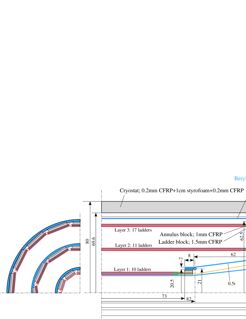
In order to make a reliable detector simulation for evaluation of the performance of the ILD, we have to make a realistic design of the sub-detectors. Concerning the vertex detector in ILD, there are several options for the sensors [2], such as CMOS sensors, DEPFET sensors, as well as FPCCD sensors. All sensor options, however, have the same sensor thickness of 50 m and the same configuration can be used for the mass production of the simulation data. Detailed difference between sensor options such as pixel size or point resolution can be taken into account at the digitization and reconstruction phase. Based on this scheme, we decided to make a mechanical design of the ILD vertex detector to be used in ILD detector simulation model (MOKKA) common to all sensor options.
Figure 3 shows the overall mechanical design of the ILD vertex detector. The design is based on the SLD vertex detector design, but double sided ladder is assumed for ILD. Each ladder consists of 50 m thick silicon sensors and readout electronics chips put on both sides of ultra light 2-mm thick substrate made of carbon foam or silicon carbide foam. Material budget of a ladder is 0.3%/ladder0.15%/layer. Flexible printed circuit (FPC) cables coming from ladders are connected to junction circuits outside the cryostat using micro connectors. The junction circuit including clock drivers, data suppression circuits, optical fiber drivers, etc. are placed surrounding the beam pipe. Compared with the old model used for the simulation study in ILD Letter of Intent (LOI) [2], material budget in forward region is increased.
4 Summary
So far, starting from 24 m-pixel fully depleted CCD, small (6 mm6 mm) FPCCD prototypes have been manufactured four times, and finally 6 m-pixel FPCCD has been developed. Design of the first large prototype of FPCCD is in progress and the prototype chips will be delivered in JFY2012. Technology to make CCD wafers thinned down to 50 m has been established. R&D for cooling system using 2-phase CO2 is being carried out in collaboration with LC-TPC, Belle-II vertex, and KEK cryogenic groups. A tentative common mechanical design has been made to be implemented into the ILD simulation model.
Acknowledgments
We would like to thank the members of CO2 collaboration of KEK Detector Technology Project for R&D of the 2-phase CO2 cooling system. This work is partly supported by Grant-in-Aid for Creative Research No.18GS0202 and Grant-in-Aid for Specially Promoted Research No. 23000002 by Japan Society for Promotion of Science (JSPS). This work is also partially supported by KEK Detector Technology Project.
References
- [1] Y. Sugimoto, Proceedings of International Linear Collider Workshop LCWS05, Stanford, CA, March 2005, pp.550-554.
- [2] T. Abe et al., ILD Letter of Intent, KEK Report 2009-6.
- [3] E. Kato et al., arXiv:1202.3017[physics.ins-det] (2012).
- [4] Y. Sugimoto, Proceedings of International Linear Collider Workshop LCWS07, DESY, Hamburg, May 2007, pp.483-485.
- [5] Y. Sugimoto et al., arXiv:0902.2067[physics.ins-det] (2009).
- [6] Y. Sugimoto et al., arXiv:1007.2471[physics.ins-det] (2010).