Thermoelectric Properties of Silicon Carbide Nanowires with Nitrogen Dopants and Vacancies
Abstract
The thermoelectric properties of cubic zincblend silicon carbide nanowires (SiCNWs) with nitrogen impurities and vacancies along [111] direction are theoretically studied by means of atomistic simulations. It is found that the thermoelectric figure of merit ZT of SiCNWs can be significantly enhanced by doping N impurities together with making Si vacancies. Aiming at obtaining a large ZT, we study possible energetically stable configurations, and disclose that, when N dopants locate at the center, a small number of Si vacancies at corners are most favored for n-type nanowires, while a large number of Si vacancies spreading into the flat edge sites are most favored for p-type nanowires. For the SiCNW with a diameter of 1.1 nm and a length of 4.6 nm, the ZT value for the n-type is shown capable of reaching 1.78 at 900K. The conditions to get higher ZT values for longer SiCNWs are also addressed.
pacs:
73.63.-b, 62.23.Hj, 61.46.KmI Introduction
Recent studies on the thermoelectric cooling and power generation by semiconductors as solid-state portable energy converters are prosperous, and there has been a great leap in both theoretical and experimental techniques. review1 ; review2 Practical applications require that the thermoelectric figure of merit ZT should be greater than 1.5 (e.g. Ref. review2, ). It is conceived that one of main approaches to promote ZT is to utilize low-dimensional semiconductor materials. 2D ; 1D For one-dimensional (1D) quantum wires, as the scattering of confined electrons is dramatically avoided while the phonons are strongly scattered off the surface, the ZT could be significantly enhanced, 1D which was supported experimentally in doped rough silicon nanowires (SiNWs), SiNW Bi2Te3 nanowires Bi2Te3 and Bi nanowires. Bi1 ; Bi2
On the other hand, silicon carbide (SiC) materials are attracting much attention for their thermoelectric properties. The nonmetallic semiconductor SiC shows excellent mechanical properties, SiCcomposite chemical durability, and in particular, the high temperature stability. Owing to its wide bandgap and low intrinsic carrier concentration, the semiconducting behavior of SiC can be kept at temperatures much higher than the case of Si, thus resulting in a higher operation temperature tolerance for SiC nanodevices. SiCNW Considering also the fact that an effective recovery of waste heat from vehicle exhaust requires an operating temperature about 350 ∘C, review2 and other applications such as high-temperature media-compatible flow sensors, SiCsensor one can see that it is quite necessary to exploit the thermoelectric properties of low-dimensional SiC materials.
As early as in 2003, Yoshida et al. have successfully doped N and B into 300 m thick SiC film that contains Si and C vacancies, and observed that with N dopants, the power factor of the SiC film is raised nearly one order of magnitude at 973 K. SiCfilm For SiC nanowires (SiCNWs), the techniques of fabrication SiCNW and measurements measurement have been remarkably improved recently, and theoretical analyses on structural properties, structure mobility, mobility thermal conductivity, tconductivity etc., were also carried out for a few cases. These studies suggest that it is prospective to obtain nice thermoelectric performance on SiCNWs. To achieve this goal, the detailed simulations and studies on thermoelectric properties of SiCNWs are really essential, which is however sparse in literature.
In the present work, we will focus on the 3C-SiCNWs doped with N impurities and vacancies along [111] direction with an energetically favorable hexagonal cross section, structure which are readily fabricated. 3C1 ; 3C2 We investigate the structures, electronic and phonon transmissions, and analyze the effect of defects on the thermoelectric performance of SiCNWs. It is found that the thermoelectric figure of merit ZT of SiCNWs can be significantly enhanced by doping N impurities together with making Si vacancies. An optimal doping strategy is suggested for both n-type and p-type SiCNWs.
This paper is organized as follows. In Sec. II, the simulation method and details will be described. In Sec. III, the structural stability of SiCNWs with defects will be discussed. The electronic structures and transport properties of SiCNWs with various defects are shown in Sec. IV. In Sec. V, the phonon transport properties of SiCNWs will be analyzed. In Sec. VI, the effects of different defects on thermoelectric transport properties of SiCNWs are presented. Finally, a summary will be given.
II Calculational Method
Structural optimizations are performed by the SIESTA code, siesta which is based on the density functional theory (DFT) DFT with norm-conserving pseudopotentials T-M and linear combinations of atomic orbitals. The optimizations are spin-polarized, employing double-zeta polarized basis sets within generalized gradient approximation (GGA) expressed by PBE functional. PBE The energy cutoff is 180 Ry, and the force tolerance criterion is 0.04 eV/ for structural relaxation. The separation between neighboring nanowire surfaces is 15 .
The electron transmission spectra are calculated by TRANSIESTA code, transiesta based on the Landauer-Büttiker and nonequilibrium Green’s function (NEGF) formalism, Datta ; negf employing single-zeta basis sets with GGA and PBE. The energy cutoff is 100 Ry, and the convergence criterion of density matrix is 0.005. The leads of the transport model are assumed to be pristine nanowires. To calculate the mean free path (MFP) and localization length of single N dopant, the supercell between the leads is chosen to contain five unit cells with a total length of 38.5 . The three middle units together are fully relaxed, where the single N dopant is in the central unit. Following the method introduced in Refs. [MFP1, ; MFP2, ], the average scattering resistance at different positions for single dopant is defined as
| (1) |
| (2) |
where , , , , and are scattering resistance, contact resistance, conductance with dopants, conductance without dopant, the weight of different doping positions, and the number of conducting channels, respectively. The mean resistance of wire and thus the MFP can be estimated linearly by
| (3) |
where is the average dopant-dopant separation estimated from a realistic doping density. Such a linear relation is valid when the wire length is in the quasiballistic () and diffusive () regimes. In the localization regime (), the resistance increases exponentially. MFP1 ; MFP2 For 3C-SiC, the carrier concentration can be controlled in the range of 1015-1019 cm-3 (Ref. [concentration, ]). In the present work we use =40 nm corresponding to a bulk doping density about 1.51016 cm-3. The localization length is calculated by xi
| (4) |
To calculate the transport properties of the SiCNWs with different defect combinations of N dopants and vacancies, we suppose that the defects are distributed homogeneously in the units between the leads, where the length between the leads is taken as 3 units (about 2.3 nm) by default, except for the case of 6 units with particular specification. For phonon transmission, the force constant matrices are calculated by GULP code, gulp which is based on the Tersoff model of empirical potential (TEP). tersoff1 ; tersoff2 ; tersoff3 To obtain dynamical matrices, the intra-atomic elements of the force constant matrices output from GULP are replaced by the data recalculated under the condition of momentum conservation, SiNWt where the atomic masses are then included. The precision criterion of the matrices is 10-5. In terms of the dynamical matrices, the phonon transmission spectra are calculated within the Landauer-Büttiker and NEGF formalism similar to the case of electrons, following the method described in Refs. [SiNWt, ; ttransport, ; sgf, ]. It is known that the Landauer-Büttiker formalism employs a finite central region for transport. In our calculations we use the nanowires with a fixed length to get the electronic and thermal conductance from the electron and phonon transmission spectra, where the length can be eliminated in calculations of the thermoelectric figure of merit ZT that can be obtained by review1 ; SiNWte ; BiNW
| (5) |
| (6) |
| (7) |
| (8) |
| (9) |
| (10) |
where is the Seebeck coefficient, is the temperature, is the chemical potential, , and are the electronic conductance, thermal conductance of electrons and phonons, respectively, and are the phonon and electron transmission, respectively. is the power factor. Generally speaking, the closer of the chemical potential to the conduction band minimum (CBM) or the valence band maximum (VBM) is, the higher carrier concentration of electrons or holes is. SiNWte ; GeSiNWte The nonlinear effects such as electron-electron, phonon-phonon and electron-phonon interactions are ignored for simplicity in the present work. ttransport ; SiNWte
III Structural Stability with Defects
In experimental and theoretical studies on SiCNWs, the most reported one is the cubic zincblend 3C()-SiCNWs along [111] direction, because it can be deposited on Si. SiCNW ; SiCNWfet ; structure ; modulus2 As a typical model for simulation, we choose the ultrathin 3C-SiCNWs with a diameter of 1.1 nm and a hexagonal cross section to investigate their structural and thermoelectric properties. As shown in Fig. 1(a), one unit cell of the pristine SiCNW contains 37 Si and 37 C atoms in pairs along the [111] direction, and 42 H atoms are covered on surface to saturate the dangling bonds of Si and C atoms. Following from the simulations on SiNWs, SiNWt ; SiNWte ; SiNWH it is necessary to include H atoms as surface passivation for electronic calculations, while the H atoms could be omitted for phonon calculations that produces a small deviation no larger than 3%. SiNWt ; SiNWte
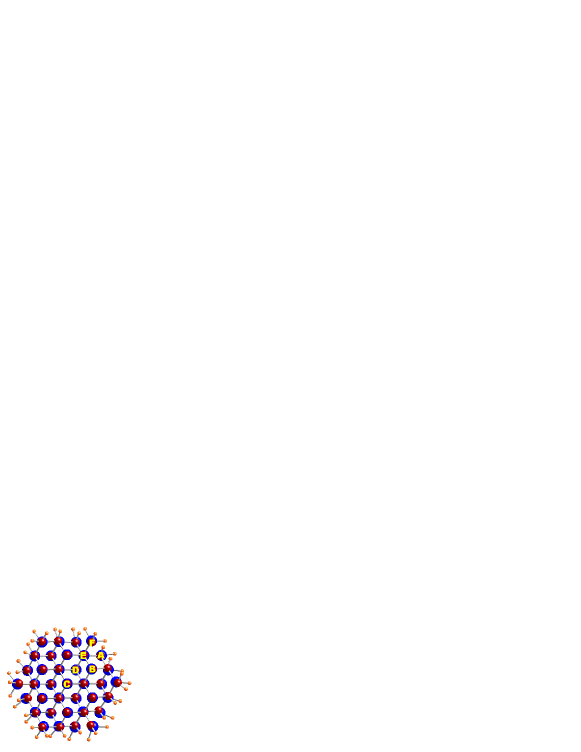
The properties of doping one N or B atom per unit cell into the 3C-SiCNW have been theoretically investigated in Ref. [SiCNWdoping, ]. It reveals that it is more favorable to dope N atom substituting C than substituting Si atom, the energetically most stable doping site of N is at the center of the SiCNW (site C), and the inner doping positions of B, C and D are energetically more favorable than the near-surface position E and surface positions A and F, SiCNWdoping which is in agreement with our results.
We go on investigating the combined defects with N impurities and vacancies in the SiCNW. Such kinds of defects have been successfully implanted in SiC film, SiCfilm but no details on the distribution of doping positions were given. Here, the sites of impurities in the SiCNW are marked in Fig. 1. For clarity, the case that dopes one N atom per unit cell substituting the C atom at the center (site C) is labeled as SiCNWNCH; the case that dopes two N atoms substituting C atoms at sites C and A is labeled as SiCNWNCAH; the case that dopes one N at site C and one Si vacancy at site A with saturated passivation by H atoms is labeled as SiCNWNCVH, where the case with unsaturated passivation leaving 3 dangling bonds per unit cell is labeled as SiCNWNCVh(3), and leaving 1 dangling bond as SiCNWNCVh(1); the case that dopes one N at C site and three Si vacancies at three corresponding A sites with saturated passivation is labeled as SiCNWNCVH; and so on. When vacancies are included, a supercell containing two units is employed where neighboring units have the interlaced vacancies at the corresponding symmetrical sites. Note that one dangling bond per unit cell in SiCNWNCAH is not left by the SiC, but by the N dopant at the surface site A.
The formation energy Ef averaged over one unit cell is calculated by SiCNWdoping ; formation1 ; formation2
| (11) |
where Etot(D) and Etot(pure) represent the total energy with and without the defects (D), respectively, is the number increment of atoms induced by the defects, is the chemical potential, and . At Si-rich, N-rich and H-rich limit, the chemical potentials are , , and , respectively. The formation energies of several typical cases are shown in Table I.
| NW with defect | Ef(eV) | NW with defect | Ef(eV) |
|---|---|---|---|
| SiCNWNCH | -0.75 | SiCNWNCVH | 1.86 |
| SiCNWNCAH | -1.38 | SiCNWNCVH | -1.37 |
| SiCNWNCDH | -1.36 | SiCNWNCVH | -2.51 |
| SiCNWNCVh(1) | -0.01 | SiCNWNCVH | -1.26 |
| SiCNWNCVh(3) | 4.33 | SiCNWNCVH | -1.45 |
| SiCNWNCVh | 3.89 | SiCNWNAVH | -0.86 |
One may see that SiCNWNCVh(3), SiCNWNCVh and SiCNWNCVH have very large positive values of Ef, implying that these structures with defects are unlikely to form because of too much formation energy needed. formation1 ; formation2 SiCNWNCVh(1) has an Ef very close to zero, showing that it is also unstable. All of the remaining cases have negative Ef, which are energetically favorable and would be likely to be fabricated. The common ground of these cases is that all the Si and C atoms get saturated passivation. It appears that the Si vacancies favor the surface sites where it is easy to passivate all the dangling bonds, thus enabling those structures stable. Comparing SiCNWNAVH with SiCNWNCVH, in presence of the Si vacancy on the surface, the N dopant is obviously more favorable for the center site than the surface. Comparing SiCNWNCAH and SiCNWNCDH, SiCNWNCVH and SiCNWNCVH, we note that in presence of one N dopant stable at the center, the Ef differences between them are as small as 0.02 eV and 0.11 eV, respectively, suggesting that their corresponding concentrations in the SiCNWs are close. However, Ef of SiCNWNCVH is much lower than that of SiCNWNCVH by 1.06 eV. It is clear that the location of Si vacancies prefers energetically the corner (site F) to the flat edge (site A).
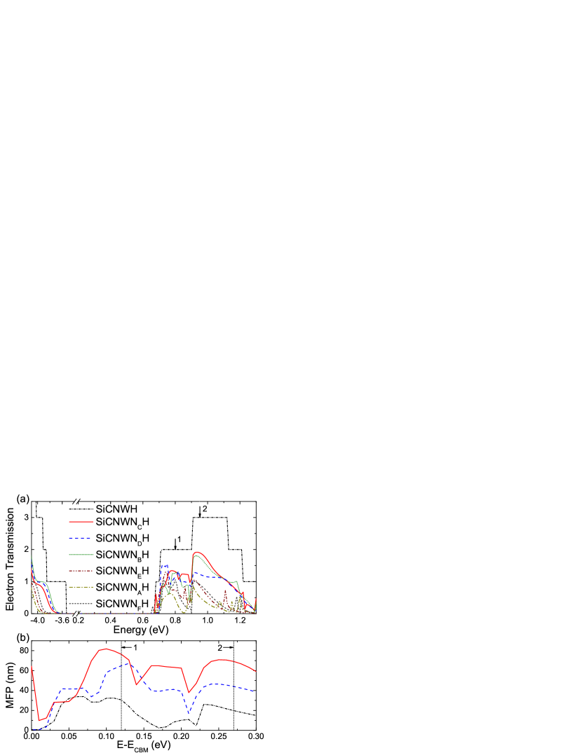
To estimate the MFP and the localization length for the case with single N dopant substituting one C atom, the electronic transmission spectra of the cases with one single N atom doped at different positions are calculated, as shown in Fig. 2(a). Except for the spectra very close to the CBM, the spectra associated with the three inner doping positions B, C and D are obviously higher than those of the surface and near-surface positions A, E and F. In Fig. 2(b), the MFPs for the structures with single N dopant of (i) the average of all six doping positions, (ii) the average of the positions B, C and D, and (iii) the position C are presented, where a dopant-dopant separation is taken as 40 nm. The energetically stability of these three cases strengthens from (i) to (iii) SiCNWdoping . From Eqs. (3) and (4), we find that at E-ECBM=0.12 with the conducting channels N=2, for case (i), (ii) and (iii), =30.58, 64.78 and 76.35 nm, =45.87, 97.17 and 114.53 nm, respectively; and at E-ECBM=0.27 with N=3, =19.84, 44.05 and 69.22 nm, =39.69, 88.10 and 138.44 nm, respectively. It indicates that for single N dopant, the structures with energetically favorable inner doping positions have the MFPs and localization lengths larger than those with the surface positions that are energetically unfavorable.
IV Electronic Structure and Transport

The electronic band structures of SiCNWH, SiCNWNCH and SiCNWNCVH are shown in Fig. 3, where the zero point of energy is set to the VBM of the defect-free SiCNWH. From Fig. 3(a), one may see that SiCNWH has a direct gap, where the Fermi level locates in the band-gap. Fig. 3(b) manifests that the N dopant in SiCNW is an n-type defect, which significantly changes the bottom of the conduction band, and the Fermi level is cross this CBM. SiCNWdoping Therefore, the N impurity gives an essential contribution to the electronic transport. It is noted that the Fermi level of SiCNWNCH is 0.12 eV lower than the CBM of the defect-free SiCNWH, and the degeneracy of the bands of SiCNWNCH is also lower than that of SiCNWH. Similar changes occur for the case of SiCNWNCVH shown in Fig. 3(c). The n-type defects introduce more electron carriers and stronger scattering of electrons.
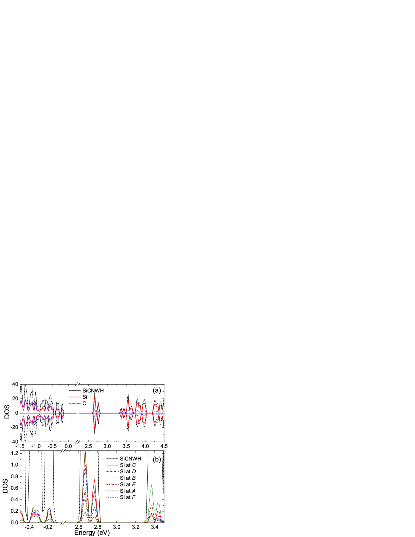
Fig. 4(a) shows the density of states (DOS) of the defect-free SiCNWH, which is calculated with a spin-polarized code. It can be seen that the electronic band is spin unpolarized, and the Si atoms contribute overwhelmingly to the DOS at the bottom of the conduction band. The peaks of the projected DOS (PDOS) of Si and C atoms totally overlap, and their relative magnitudes are inverse in the valence and conduction bands, indicating that the Si and C atoms bond with each other. The PDOS of one Si atom at different positions is presented in Fig. 4(b). For the two peaks of DOS around 2.7 eV, the PDOS of the system with one Si atom at position B is almost coincident with that of Si at position C in the lower peak and with that of Si at position D in the higher peak. The PDOS of Si at positions A and F in the higher peak are also nearly coincident. The PDOS of Si at inner positions B, C and D are significantly higher than those at outer positions E, F and A.
It is interesting to note that for the peak of electronic transmission spectra from 0.8 to 1.2 eV in Fig. 2(a), the spectra of the system with N dopant substituting C atom at inner positions B, C and D are obviously higher than those at outer positions E, F and A, which is qualitatively consistent with the PDOS of different Si atoms for the peak around 2.7 eV in Fig. 4(b). When the N dopant substitutes one C atom in SiCNWs, the neighboring Si atoms connected by bonds will obtain extra electrons from the dopants. The PDOS of the N dopant will spread to the valence and conduction bands similar to the PDOS of Si atoms. SiCNWdoping At the bottom of the conduction band, the Si atoms at inner positions contribute to the majority of the DOS, so the N defects at inner positions contribute electrons to the bottom of conduction bands more than those doped at outer positions. From these results one may deduce that for the peak of electronic transmission spectra at the bottom of conduction band, the spectra with N defect at inner positions could be higher than those at outer positions, which is just the results shown in Fig. 2(a).
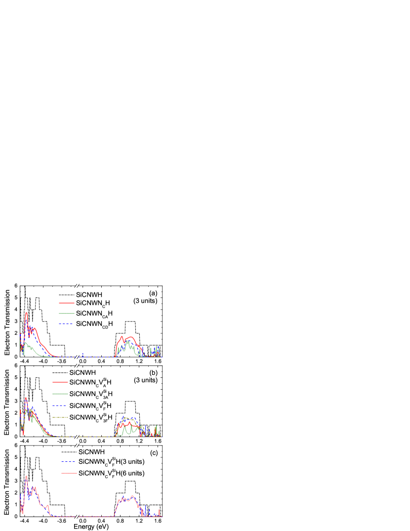
To probe the transport properties of SiCNWs with defects, besides the pure SiCNWH and SiCNWNCH that is energetically the most stable case for the NC defect, SiCNWdoping SiCNWNCAH, SiCNWNCDH, SiCNWNCVH, SiCNWNCVH, SiCNWNCVH and SiCNWNCVH are selected as relatively stable examples from the cases with different doping sites.
The electronic transmissions of SiCNWs with various defects are given in Fig. 5. As shown in Fig. 5(a), for SiCNWNCH, at the bottom of conduction band the electron transmission spectrum shrinks slightly from the spectrum of SiCNWH, while at the top of valence band the hole transmission spectrum has a significant shrink from that of SiCNWH. For SiCNWNCAH and SiCNWNCDH the transmission spectra go on shrinking from SiCNWNCH, and the shrink is extraordinarily evident for the hole transmission of SiCNWNCAH that has one surface dangling bond left by the N dopant at site A. So the N impurities in the SiCNW induce stronger scattering of electrons, which overcomes the effect of the increase of electron carriers by the n-type doping, resulting in the decrease of electron/hole transmission. More dopants of N will lead to a greater decrease of transmission.
The cases of SiCNWs with implantation of saturated Si vacancies on surface in addition to the N dopant at center are shown in Fig. 5(b). The spectra of SiCNWNCVH and SiCNWNCVH with more Si vacancies are a bit lower than those of SiCNWNCVH and SiCNWNCVH owing to the stronger scattering by the vacancies. Comparing the spectra of SiCNWNCVH, SiCNWNCVH, SiCNWNCVH and SiCNWNCVH in Fig. 5(b) with that of SiCNWNCH in Fig. 5(a), we find that in presence of the central N dopant, for the hole transmission with surface Si vacancies at either the corner (site F) or the flat edge (site A) site, and for the electronic transmission with surface Si vacancies at the corner F, the spectra change little from that of SiCNWNCH, revealing that the electron or hole scattering are not significantly strengthened by the vacancies. Consequently, the MFP and the localization length of SiCNWNCVH and SiCNWNCVH would have values close to those of SiCNWNCH due to their similar transmission spectra.
Fig. 5(c) compares the electronic transmission spectra of SiCNWNCVH with 3 and 6 units in length. The two spectra are quite close, and the spectrum of 6 units has a larger gradient at the edge of the bands. It reveals that for SiCNWNCVH, the effects of increasing electron carriers and strengthening the electron scattering by the n-type defects get balanced so that the electronic transmission changes little, as the wire length increases.
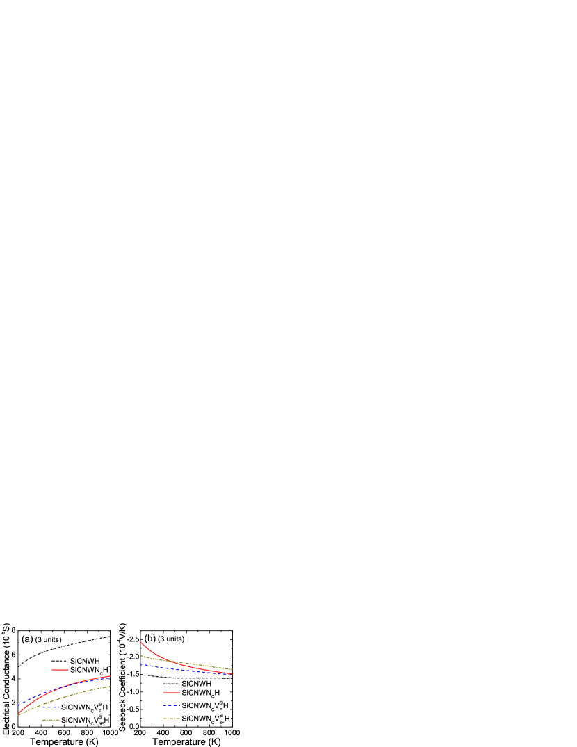
With the electronic transmission spectra, the electrical conductance , the Seebeck coefficient and the power factor can be calculated by means of Eqs. (7) and (9). Generally, the maximum of ZT is achieved when the chemical potential is around the CBM for electrons and the VBM for holes SiNWte . The temperature dependences of and are presented in Figs. 6(a) and (b) for pure SiCNWH, SiCNWNCH, SiCNWNCVH and SiCNWNCVH, respectively. These four cases are chosen owing to their relatively large transmission of electrons as seen from Figs. 5(a) and (b). Here is set to 0.675 eV, which is the bottom of the electron transmission spectrum of pure SiCNWH. As shown in Figs. 6(a) and (b), the differences among SiCNWNCH, SiCNWNCVH and SiCNWNCVH are small, unveiling that the effect of the increase of electron carriers and the enhancement of electron scattering induced by more Si vacancies are nearly balanced. No matter the defects that include Si vacancies or not, are significantly lower than those of pure SiCNWH due to the electron scattering by the N dopants. Moreover, it can be seen that for all four cases, as temperature increases from 200 to 1000 K, the electrical conductance increases while the magnitude of negative Seebeck coefficient decreases. When temperature is higher than 400 K, the changes of both and become slow.
V Phonon Transport

To investigate the properties of phonon transport, Fig. 7 gives the phonon band structures of SiCNWH, SiCNWNCH and SiCNWNCVH. It is uncovered that the degeneracy of phonon bands is lowered either by doping N at the center into SiCNWH, or by doping Si vacancies at the corner site F into SiCNWNCH, suggesting that the phonon scattering is strengthened. However, the number and the energy ranges of the phonon bands are nearly unchanged among these cases, which is in contrast to the defect bands in the gap of electronic band structures (Fig. 3).
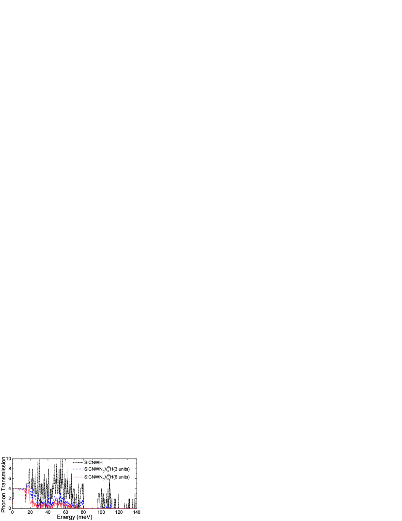
As shown in Fig. 8, the phonon transmission of pure SiCNWH is equal to 4 at the low energy range close to zero, which corresponds to the four acoustic modes of phonons in nanowires. Compared with SiCNWH, the phonon transmission spectrum of SiCNWNCVH is obviously lower, and above 80 meV, the phonon transmission decreases near to zero. When the wire length increases from 3 to 6 units, the phonon transmission of SiCNWNCVH is further lowered. In contrast to the results in Fig. 5(c) that the electronic transmission of SiCNWNCVH change little from 3 to 6 units in length, there are no factors to balance the strengthening of phonon scattering by the defects, and the phonon transmission of SiCNWNCVH decreases significantly as the wire length increases.
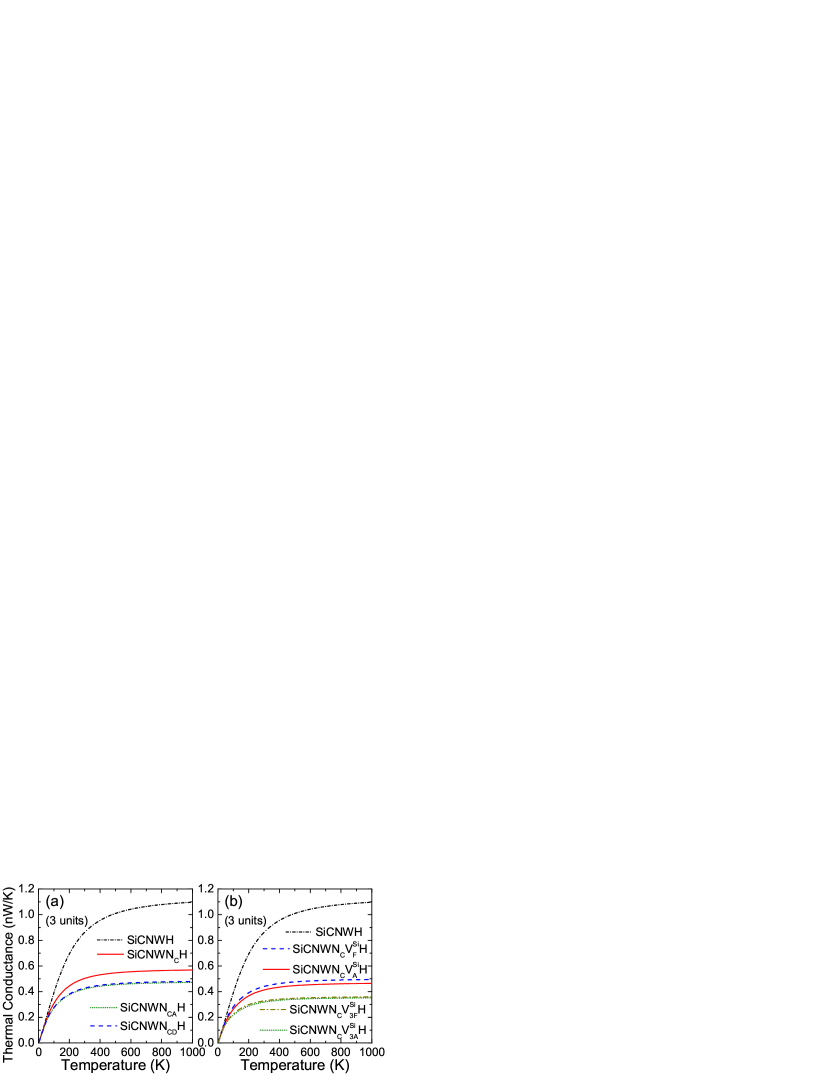
Fig. 9 presents the lattice thermal conductance for various cases in the temperature range of 0-1000 K. first goes up rapidly and then increases slowly when temperature is higher than 300 K. It is seen that the decreases as the defects of N or Si vacancy increase. The differences of between SiCNWNCAH and SiCNWNCDH, SiCNWNCVH and SiCNWNCVH, SiCNWNCVH and SiCNWNCVH are small, which are 0.01 nW/K, 0.03 nW/K and 0.01 nW/K at 1000 K, respectively. It indicates that the same doping concentration at different doping sites leads to very similar thermal conductance. Comparing Fig. 6 with the corresponding cases in Fig. 9, one may see that in the presence of N dopants or Si vacancies, both and will decrease from the values of pure SiCNWH, but the amplitude of is decreased more remarkably than that of .
VI Thermoelectric Transport
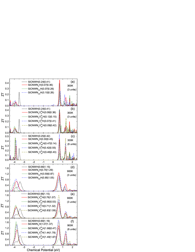
Combining the results of electron and phonon transport, the thermoelectric figure of merit ZT is calculated as a function of the chemical potential SiNWte by Eqs. (5)-(10) at 300 K and 900 K, respectively, as shown in Fig. 10. Comparing Figs. 10 and 5, the maximum of ZT occurs when the chemical potential reaches the VBM for p-type SiCNWs or the CBM for n-type SiCNWs, where the electronic transmission changes dramatically.
For n-type SiCNWs, at 300K or 900K, it is clear that in Figs. 10(a), 10(b), 10(d) and 10(e), the cases of SiCNWNCH, SiCNWNCVH and SiCNWNCVH can induce obvious enhancements of the ZT. For other cases the ZT is even lower than that of SiCNWH. Among SiCNWNCH, SiCNWNCVH and SiCNWNCVH, their relative magnitudes of ZT change as the length increases from 3 to 6 units, as shown in Figs. 10(c) and 10(f). For a length of 6 units, the n-type ZT maximum of SiCNWNCH, SiCNWNCVH and SiCNWNCVH are 0.45, 0.55 and 0.43 at 300 K, 1.37, 1.78 and 1.67 at 900 K, respectively. Thus, the ZT maximum for n-type is given by SiCNWNCVH, containing the defects of one N dopant at the center and one Si vacancy at the corner per unit cell. Neither more N dopants such as SiCNWNCDH nor more Si vacancies such as SiCNWNCVH are beneficial. In general, to avoid the ZT dropping from the maximum of SiCNWNCVH to the value of SiCNWNCVH or others, it is preferable to dope N impurities limited at the center and a small quantity of Si vacancies limited at the corners (F sites), which is energetically favorable. Such a distribution of Si vacancies at the corners strengthens the phonon scattering dramatically while it influences little on the electron scattering.
For SiCNWNCH and SiCNWNCVH, it was shown in Fig. 3 that their Fermi levels are about 0.1 eV lower than the CBM of the defect-free SiCNWH. The Fermi level equals to the chemical potential at zero temperature. As manifested in Fig. 10, because the highest peaks of ZT for n-type accumulate around the CBM of SiCNWH, the corresponding chemical potential at finite temperature will lead to a ZT value very close to the maximum of ZT for n-type.
For p-type SiCNWs, among the cases in Figs. 10(a), 10(b), 10(d) and 10(e), the maximum of ZT of SiCNWNCDH is larger than that of SiCNWNCAH. Considering the tiny difference of formation energy Ef between SiCNWNCAH and SiCNWNCDH, the larger ZT of SiCNWNCDH is hard to maintain. On the other hand, the differences of ZT among SiCNWNCVH, SiCNWVH, SiCNWNCVH and SiCNWNCVH are quite small, while the energetically most favorable one is SiCNWNCVH. All these four cases have significant ZT enhancements in Figs. 10(c) and 10(f), and relatively, the cases with more Si vacancies have larger ZT. For the best two cases, SiCNWNCVH and SiCNWNCVH with a length of 6 units, the p-type ZT maximum is 0.47 and 0.46 at 300 K, 1.66 and 1.49 at 900 K, respectively, which are obviously larger than the values of SiCNWH, as shown in Figs. 10(c) and 10(f). Therefore, it is preferable to dope N impurities stable at the center and a large quantity of Si vacancies not only at the corners (F sites) but also spreading to the flat edges (A sites). However, the p-type performance depends on the ingredient of the p-type dopants which is not addressed in the present work.
It should be noted that the selected cases cannot cover all positions and concentrations of the defects. However, the performances affected by various defects are reflected in the ZT curves of these selected interesting cases as functions of . For instance, as displayed in Figs. 10(a) and 10(d), for the n-type the peaks of ZT for SiCNWNCH, SiCNWNCAH and SiCNWNCDH appear at 0.675, 0.695 and 0.725 eV at 300 K, 0.595, 0.635 and 0.665 eV at 900 K, respectively. Compared with SiCNWNCH, SiCNWNCAH and SiCNWNCDH have more N dopants leading to a higher carrier concentration of electrons and a larger chemical potential. The ZT maximums are listed in the brackets in the figure legends. It can be seen that for the n-type SiCNWNCH, as the chemical potential increases, the ZT values on the right side of the highest peak are close to the ZT maximums of SiCNWNCAH and SiCNWNCDH. Thus, as seen in Figs. 10(c) and 10(f), even if the ZT curves of SiCNWNCAH and SiCNWNCDH are not shown, for the cases with different doping concentrations of N, the corresponding ZT could be approximately estimated from the ZT curve of SiCNWNCH.
From Figs. 10(c) and 10(f), it is clear that the ZT of 6 units is larger than the ZT of 3 units for all the cases under interest. As an example, the electronic and phonon transmission spectra of SiCNWNCVH with different lengths have been illustrated in Figs. 5(c) and 8. From the discussions in Figs. 3, 5(c), 6, 8 and 9, we know that for the cases of n-type doping, the effect of strengthening the electron scattering is balanced by the increase of the electron carriers for electronic transmission, while the strengthening of the phonon scattering is unbalanced. Thus, as the wire length increases from 2.3 to 4.6 nm, the electronic transmission change little while the phonon transmission decreases significantly, leading to the increase of ZT value.
In Sec. III, the localization length of the case with N dopant was estimated to be greater than 100 nm at the bottom of conduction band. Doping Si vacancies at the corners into the N doped SiCNW will not change the localization length obviously, for SiCNWNCVH has an electronic transmission spectrum close to SiCNWNCH. With a wire length smaller than the localization length, the electronic resistance will increase along with the wire length linearly. MFP1 ; MFP2 Moreover, it has been reported in the case of SiNWs with a diameter of 1.2 nm that the thermal conductance keeps decreasing dramatically before the length increases over 50 nm, and after this length the thermal conductance decreases almost linearly. SiNWte In this sense, for the nanowires such as SiCNWNCVH, the tendency of ZT enhancement is probable to be kept not only for the wire length from 2.3 nm to 4.6 nm, but also for a wire length of about 50 nm. As a result, there is still a large room to expect a further enhancement of ZT when the length increases from 4.6 nm, and a large ZT can be maintained within the localization length.
VII Summary
In summary, the structural stability and the thermoelectric properties of SiCNWs with N dopants and vacancies are investigated by means of the density functional calculations. Our studies show that the central (C) site for N dopants is energetically the most stable. When the defects contain both N impurities and vacancies, the most favorable configuration is that the N impurities are at the center while the Si vacancies locate at the corners (F) with all the dangling bonds passivated. Aiming at obtaining a large thermoelectric figure of merit ZT, with N dopants at the center, a small quantity of Si vacancies limited at the corners is most favored for n-type, while a large quantity of Si vacancies spreading to the flat edge (A) sites is most favored for p-type wires.
For the SiCNW as quantum wires along [111] with a diameter of 1.1 nm and a length of 4.6 nm, the ZT maxima at 900 K are found to be about 1.78 for n-type and 1.66 for p-type, respectively. The ZT maximum of n-type can be reached by the present n-type doping of N impurities and Si vacancies, but for p-type it depends on whether or not there are proper p-type dopants. As long as the decrease of phonon transmission with the increase of length is far more rapid than the decrease of electronic transmission, higher ZT values may be expected for SiCNWs longer than 4.6 nm. Based on the reduced model of quantum wires for simulation, the present findings may shed light on the enhancement of the ZT values by taking advantage of N dopants and surface Si vacancies in SiCNWs, that is especially favorable for the thermoelectric performance at high temperature in applications.
Acknowledgements.
We are grateful to Q. B. Yan, X. L. Sheng, X. Chen, H. J. Cui and Eric Germaneau for useful discussions. All calculations are completed on the supercomputer MagicCube (DAWN5000A) in Shanghai Supercomputer Center. This work is supported in part by the MOST, the NSFC (Grant Nos. 90922033, 10934008, and 10974253) and the CAS.References
- (1) F. J. DiSalvo, Science 285, 703 (1999).
- (2) L. E. Bell, Science 321, 1457 (2008).
- (3) L. D. Hicks and M. S. Dresselhaus, Phys. Rev. B 47, 12727 (1993).
- (4) L. D. Hicks and M. S. Dresselhaus, Phys. Rev. B 47, 16631 (1993).
- (5) A. I. Hochbaum, R. Chen, R. D. Delgado, W. Liang, E. C. Garnett, M. Najarian, A. Majumdar, and P. Yang, Nature 451, 163 (2008).
- (6) J. Lee, S. Farhangfar, J. Lee, L. Cagnon, R. Scholz, U. Gösele, and K. Nielsch, Nanotechnology 19, 365701 (2008).
- (7) W. Shim, J. Ham, K. Lee, W. Y. Jeung, M. Johnson, and W. Lee, Nano Lett. 9, 18 (2009).
- (8) D. Gitsu, L. Konopko, A. Nikolaevaa, and T. E. Huber, Appl. Phys. Lett. 86, 102105 (2005).
- (9) L.-D. Zhao, B.-P. Zhang, J.-F. Li, M. Zhou, W.-S. Liu, J. Liu, J. Alloy. Compd. 455, 259 (2008).
- (10) K. Zekentes and K. Rogdakis, J. Phys. D: Appl. Phys. 44, 133001 (2011).
- (11) N. G. Wright and A. B. Horsfall, J. Phys. D: Appl. Phys. 40, 6345 (2007).
- (12) X. H. Wang, A. Yamamoto, K. Eguchi, H. Obara, and T. Yoshida, Science and Technology of Advanced Materials 4, 167 (2003).
- (13) K. M. Lee, T. Y. Choi, S. K. Lee, and D. Poulikakos, Nanotechnology 21, 125301 (2010).
- (14) Z. Wang, X. Zu, F. Gao, and William J. Weber, Phys. Rev. B 77, 224113 (2008).
- (15) K. Rogdakis, S. Poli, E. Bano, K. Zekentes and M. G. Pala, Nanotechnology 20, 295202 (2009).
- (16) N. Papanikolaou, J. Phys.: Condens. Matter 20, 135201 (2008).
- (17) E. W. Wong, P. E. Sheenhan, and C. M. Lieber, Science 277, 1971 (1997).
- (18) T-Y. Zhang, M. Luo, and W. K. Chan, J. Appl. Phys. 103, 104308 (2008)
- (19) P. Ordejón, E. Artacho, J. M. Soler, Phys. Rev. B 53, 10441 (1996).
- (20) W. Kohn and L. J. Sham, Phys. Rev. 140, A1133 (1965).
- (21) N. Troullier and J. L. Martins, Phys. Rev. B 43, 1993 (1991).
- (22) J. P. Perdew, K. Burke, and M. Ernzerhof, Phys. Rev. Lett. 77, 3865 (1996).
- (23) M. Brandbyge, J.-L. Mozos, P. Ordejón, J. Taylor, and K. Stokbro, Phys. Rev. B 65, 165401 (2002).
- (24) S. Datta, Electronic Transport in Mesoscopic Systems (Cambridge University Press, 1995).
- (25) Y. Meir and N. S. Wingreen, Phys. Rev. Lett. 68, 2512 (1992).
- (26) T. Markussen, R. Rurali, A.-P. Jauho, and M. Brandbyge, J. Comput. Electron 7, 324 (2008).
- (27) T. Markussen, R. Rurali, A.-P. Jauho, and M. Brandbyge, Phys. Rev. Lett. 99, 076803 (2007).
- (28) Y. Kumashiro et al., Electric Refractory Materials, Chapter 19, (Marcel Dekker, 2000).
- (29) C. W. J. Beenakker, Rev. Mod. Phys. 69, 731 (1997).
- (30) J. D. Gale, J. Chem. Soc. Faraday Trans. 93, 629 (1997).
- (31) J. Tersoff, Phys. Rev. Lett. 61, 2879 (1988).
- (32) J. Tersoff, Phys. Rev. B 38, 9902 (1988).
- (33) F. de Brito Mota, J. F. Justo, and A. Fazzio, J. Appl. Phys. 86, 1843 (1999).
- (34) T. Markussen, A.-P. Jauho, and M. Brandbyge, Nano Lett. 8, 3771 (2008).
- (35) J.-S. Wang, Jian Wang, and J. T. Lü, Eur. Phys. J. B 62, 381 (2008).
- (36) D. H. Lee and J. D. Joannopoulos, Phys. Rev. B 23, 4997 (1981).
- (37) T. Markussen, A.-P. Jauho, and M. Brandbyge, Phys. Rev. B 79, 035415 (2009).
- (38) Y.-M. Lin, X. Sun, and M. S. Dresselhaus, Phys. Rev. B 62, 4610 (2000).
- (39) X. Chen, Y. Wang, and Y. Ma, J. Phys. Chem. C 114, 9096 (2010).
- (40) K. Rogdakis, S.-Y. Lee, M. Bescond, S.-K. Lee, E. Bano, and K. Zekentes, IEEE Trans. Electron Devices 55 1970 (2008).
- (41) T.-Y. Zhang, M. Luo, and W. K. Chan, J. Appl. Phys. 103, 104308 (2008).
- (42) Z. Xu, Q.-B. Yan, Q.-R. Zheng, and G. Su, Phys. Rev. B 80, 081306(R) (2009).
- (43) I. S. S. de Oliveira and R. H. Miwa, Phys. Rev. B 79, 085427 (2009).
- (44) J. E. Northrup and S. B. Zhang, Phys. Rev. Lett. 67, 2339 (1991), Phys. Rev. B 47, R6791 (1993).
- (45) R. Qin et al., J. Phys. Chem. C 113, 9541 (2009).