Double proximity effect in hybrid planar Superconductor-(Normal metal/Ferromagnet)-Superconductor structures
Abstract
We have investigated the differential resistance of hybrid planar Al-(Cu/Fe)-Al submicron bridges at low temperatures and in weak magnetic fields. The structure consists of Cu/Fe-bilayer forming a bridge between two superconducting Al-electrodes. In superconducting state of Al-electrodes, we have observed a double-peak peculiarity in differential resistance of the S-(N/F)-S structures at a bias voltage corresponding to the minigap. We claim that this effect (the doubling of the minigap) is due to an electron spin polarization in the normal metal which is induced by the ferromagnet. We have demonstrated that the double-peak peculiarity is converted to a single peak at a coercive applied field corresponding to zero magnetization of the Fe-layer.
pacs:
74.45.+c, 74.78.Fk, 75.76.+jIn superconductor-normal metal (SN) bilayers the superconducting proximity effect is responsible for the modification of the electron density of states (DOS) and the appearence of a minigap in the normal metal Gol_Kupr_1988 . Thereby a normal metal region close to the SN-interface behaves as a genuine superconductor, i.e. there is an energy range (-,+) around the Fermi energy in which there are no available states for normal quasiparticles. This theoretical statement Gol_Kupr_1988 was proved reliably in recent measurements of the local DOS Gueron ; Courtois ; Esteve . A minigap peculiarity becomes apparent in the differential conductance (resistance) spectra of SNS junctions side by side with the superconducting gap peculiarity of superconducting electrodes Cuevas ; Giazotto . In the case of a superconductor-ferromagnet (SF) bilayer the ferromagnetic exchange splitting of the spin sub-bands results in an energy shift of the corresponding minigap, which is asymmetric for the majority and the minority spin sub-bands SFIFS , i.e. one can distinguish two minigap peculiarities in SF-DOS spectra. However, even in the case of diluted ferromagnets the exchange field is very large, so it is difficult to observe the minigap splitting on well-known proximity SF-systems like Nb-CuNi Oboznov and Nb-PdNi Kontos . In Ref. Yip , Yip first proposed to modify the DOS in SN-proximity system by applying a magnetic “Zeeman” field h. Unfortunately, it is difficult to use applied magnetic fields in real SN-experiments due to the “orbital” suppression of the superconducting electrodes. Recently, authors of Ref. Karm1 have proposed to induce a weak “exchange field”, , via diffusion of spin polarized electrons from F to N metal in NF bilayers, i.e. by using a complex NF bilayer as weak link in a S-(N/F)-S structure. In this case an “effective” exchange field which is induced in the N layer is much smaller than the intrinsic exchange field of the neighboring F-layer.
In this work, we report on the first experimental observation of the “minigap doubling” in the SNF banks of S-(N/F)-S submicron-size bridges schematically shown in Fig.1(b). The minigap doubling has been observed as double peak peculiarity in the differential resistance of planar Al-(Cu/Fe)-Al junctions fabricated by e-beam lithography and the shadow evaporation techniques.
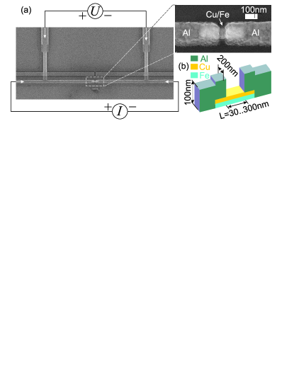
Figure 1(a) shows a scanning electron microscopy (SEM) image of one of our samples together with the measurement scheme. The submicron-scale planar junctions were fabricated by means of the electron beam lithography and in situ shadow evaporation. First, a thin (10-15 nm) iron layer is deposited onto the oxidized silicon substrate, followed by the deposition of a 60 nm thick copper layer, so that in combination the NF bilayer bridge (0.2(0.30.6) ) is formed. Subsequently, a thick aluminum layer of around 100 nm is evaporated at a second angle in order to form the superconducting leads. We fabricated samples with different separation length L between the superconducting electrodes, ranging from 30 nm to 300 nm. All transport measurements were performed using standard four-terminal method. As the specific resistance of the copper film (=4.5 cm) is much smaller than the one of the iron film (=70 cm), the main part of the current flows through the copper layer. The measurements at temperatures down to 0.3 K were performed in a shielded cryostat equipped with a superconducting solenoid. Two stages of RC filters were incorporated into the measurement system to eliminate the electrical noise.
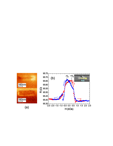
In order to check that the iron layer forms a single-domain magnetized along the S-(N/F)-S junction, reference structures with the same geometry and structure as the N/F-bilayers, but only with the ferromagnetic layer, were fabricated and subsequently investigated by means of magnetic-force-microscopy imaging (MFM). Fig.2(a) shows a MFM image of the iron bar at zero magnetic field together with the topographical image (AFM). The picture of magnetic poles is similar to the MFM images of iron nanostrips published in Ref.Hanson . According to this work we dealt with practically uniform magnetized structure. The main magnetization is directed along the long axis of rectangle but diverges from a dipolar configuration at the corners magnSim . Non-local spin-valve experiments on similar submicron iron structures indicate single-domain behavior, with coercive fields of about 200-500 Oe for magnetic fields applied along the elementBeckmannCAR . To estimate coercive field of the iron bar S-F-S (Al-Fe-Al) bridges with the same geometry but without the Cu layer were prepared. We have measured the magnetoresistance of the S-F-S bridge at T=4.2 K using in-plane magnetic field perpendicular to the Fe-bar easy-axis (Fig 2(b)). The coercive field (about 300 Oe) was determined from the maximum value of the resistance due to anisotropic magnetoresistance (AMR) effect (see, for example Ref. AMRexp ; AMRt ). The observation of a finite coercive field suggests that the magnetization configuration deviates from the single-domain structure during magnetization reversal.
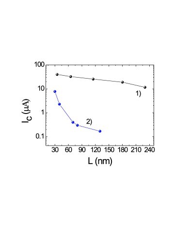
Resistive and Josephson characteristics of the planar junctions depend strongly on the spacing, L, between the aluminum electrodes as well as on the total length of Cu/Fe-bilayers that were partly overlapped by the electrodes. The characteristics and their discussion will be given in detail later SNSTG . The Josephson supercurrent was observed in structures with L from 30 nm up to 130 nm. It is important to note that the coherent Josephson transport was suppressed significantly by addition of the extra ferromagnetic layer. Fig.3 presents the dependence of the critical current Ic vs. L for Al-(Cu/Fe)-Al junctions shown in Fig.1 in comparison with Ic(L)-dependence for control Al-Cu-Al structures fabricated by the same procedure but without the additional Fe-layer. The critical currents of S-(N/F)-S junctions are much smaller than that for S-N-S junctions.
The strong suppression of the superconducting proximity effect in the N-channel of the S-(N/F)-S junction is due to the penetration of spin-polarized electrons in the copper layer from the single-domain iron strip underneath. We suppose that penetration of spin-polarized electrons through the Fe/Cu-interface provides the copper layer with an uniform spin polarization because of the small Cu-layer thickness (of 60 nm). The data of Ref.Kimura indicate that the spin-diffusion length in Cu is as large as 1 m at 1 K, that is larger than the bridge sizes.
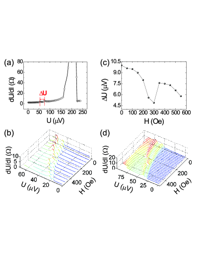
To detect DOS peculiarities of the novel double-proximity structures we measured differential current-voltage characteristics by current-driven lock-in technique as well as the dc current-voltage characteristics of the structures. Fig. 4(a) demonstrates the differential resistance vs bias voltage for Al-(Cu/Fe)-Al junction (S1) with the space L=130 nm between superconducting electrodes at T=0.4 K. The curve is symmetric with respect to the zero bias voltage, therefore only positive voltage values are shown. There are two types of peculiarities on the dU/dI(U) dependence. First one corresponds to the superconducting gap of aluminum =180 eV and the second one is a double-peak peculiarity at the subgap energy 60 eV which is much smaller than .
We suppose that the double-peak peculiarity in S-(N/F)-S transport is due to the presence of two spin-dependent minigaps in the normal metal interlayer of SNF trilayered electrodes. The most easy way to check this idea with the spin-dependent minigap origin is to change the uniform state of the ferromagnet layer magnetization. The differential resistance of the S-(N/F)-S samples was measured in presence of magnetic field H which increases from zero by small steps (see Fig.4(b)). Magnetic field was applied in plane of the sample perpendicular to the bridge, as it was for S-F-S structures shown in figure 2(b) inset. One can see that at around 300 Oe the separation between two peaks of the double-peak peculiarity decreases significantly and then goes practically to the initial value at further increase of the magnetic field. The magnetic field of about 300 Oe coincides with the coercive field of the S-F-S reference structures. While the precise magnetization state at this field is unknown, a strongly inhomogeneous state can be expected, effectively reducing the induced exchange splitting in the N layer. The dependence of the double-peak splitting U vs. applied magnetic field H is shown in figure 4(c). Moreover it was observed for some samples that the double-peak peculiarity joined to single peak at about 300 Oe (Figure 4(d)). The position of the peculiarity is shifted to low voltages with increasing magnetic field because of the suppression of superconductivity in both the aluminum electrodes and the proximity region.
Below we briefly describe calculations of the minigap splitting in a SNF-NF structure with trilayered electrode, i.e. appearance of two minigaps for majority and minority spin systems in N-layer due to proximity effect from the superconductor and magnetic proximity effect due to a contact with a ferromagnet.
For simplicity we shall discuss the case when F and N films are thin compared to the coherence lengths in these metals. Such simplification allows to obtain simple solution for the gap splitting but does not change our conclusions qualitatively. We assume that the dirty limit conditions are fulfilled in the investigated structure, therefore one can use the quasiclassical Usadel equations for Green’s functions which in -parametrization have the form:
| (1) |
Here , , are normalized Matsubara frequencies, is exchange field which vanishes in N metal, and -axes are parallel (perpendicular) to the FN interface with the origin at the boundary between the SNF trilayer and NF bilayer. Equations (1) should be supplemented by the boundary conditions Ref.KL
| (2) |
at the SN interface with and
| (3) |
at the NF interface with (we assumed that FN interface is transparent). Here and is bulk pair potential of a superconductor. is the specific resistance of SN interface, and are the resistivities and the coherence lengths of the S, F and N layers. We assume that , so that suppression of superconductivity in S electrode is negligibly small. At the free interfaces derivatives of -functions are zero in the direction of the interface normal.
The problem (1)-(3) is reduced to one-dimensional equations for Green’ functions in the NF bilayer under S electrode (for ) and Green’s functions for free FN bilayer (for ):
| (4) |
where
and , . The solutions of the above equations are
| (5) |
and normalized DOS at energy is given by:
| (6) |
where was used in calculations.
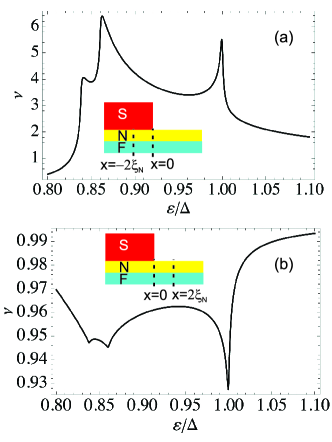
Fig.5 shows the results of calculation of total DOS (summed over both spin subbands) from Eq.6. It is seen that the peaks in DOS which for occur at energies transform to dips for . The structure at energies corresponds to minigap splitting due to effective exchange field , where are the normal-state densities of states and thicknesses of N and F layers. Interestingly, the double-peak structure at at transforms to the double-dip structure in the bridge region () at distances of the order of . The energy separation () between the peaks/dips can be estimated as For is also zero and these features merge into a single peak (dip).
In the simplest approach, the resistance of SNF-NF-NFS structure is determined by the renormalized diffusion coefficient in the NF bridge area and the dips in DOS at should lead to the double-peak structure in vs similar to the observed experimentally (see Fig.4(a)). Quantitative model is beyond the frame of our model due to complex device geometry and a number of unknown parameters.
To conclude, we have observed experimentally a manifestation of the superconducting minigap splitting in the N-layer contacted both with superconductor and ferromagnet in complex planar S-(N/F)-S system formed by Al-(Cu/Fe)-Al submicron-size bridge. Such a splitting has to exist in SF bilayers also, but it is difficult to observe it there because of the large values of the exchange field for conventional ferromagnets. It has been demonstrated that the splitting occurs only for contacts to ferromagnetic layers with uniform magnetization and disappears when the applied magnetic field close to the coercive field. DOS calculations for SNF systems have shown that the minigap splitting is really possible for parameters close to experimental ones.
We acknowledge A.V. Ustinov for support and usefull discussions. The work was encouragement by grants of Russian Academy of Sciencies and Russian Foundation for Basic Research.
References
- (1) A. A. Golubov, M. Yu. Kupriyanov, Journal of Low Temp. Phys. 70, 83 (1988)
- (2) S. Gueron, H. Pothier, N. O. Birge, D. Esteve, and M. H. Devoret, Phys. Rev. Lett. 77, 3025 (1996)
- (3) A. K. Gupta, L. Cretinon, N. Moussy, B. Pannetier, and H. Courtois, Phys. Rev. B 69, 104514 (2004)
- (4) H. le Sueur, P. Joyez, H. Pothier, C. Urbina, and D. Esteve, Phys. Rev. Lett. 100, 197002 (2008)
- (5) M. Meschke, J. T. Peltonen, J. P. Pekola, and F. Giazotto, Cond-mat. arXiv:1105.387v1 (2011)
- (6) J. C. Cuevas, J. Hammer, J. Kopu, J. K. Viljas, and M. Eschrig, Phys. Rev. B 73, 184505 (2006)
- (7) A. A. Golubov, M. Yu. Kupriyanov, Ya. V. Fominov, Pis ma v ZhETF 75, 223 (2002) [JETP Lett., 75, 190 (2002)]
- (8) V. A. Oboznov, V. V. Bol’ginov, A. K. Feofanov, V. V. Ryazanov and A. I. Buzdin, Phys. Rev. Lett. 96, 197003 (2006)
- (9) T. Kontos, M. Aprili, J. Lesueur, and X. Grison, Phys. Rev. Lett. 86, 304 (2001)
- (10) S. -K. Yip, Phys. Rev. B 62, R6127 (2000)
- (11) T. Yu. Karminskaya, M. Yu. Kupriyanov, Pis ma v ZhETF 85, 343 (2007) [JETP Lett. 85, 286 (2007)]
- (12) M. Hanson, O. Kazakova, P. Blomqvist, R. Wap̈pling, and B. Nilsson, Phys. Rev. B 66, 144419 (2002)
- (13) W. Rave and A. Hubert, IEEE Trans. Magn. 36, 3886 (2000)
- (14) D. Beckmann, H. B. Weber and H.v. Löneysen, Phys. Rev. Lett. 93, 197003 (2004)
- (15) P. P. Freitas and T. S. Plaskett, J. Appl. Phys. 67, 4901 (1990)
- (16) R. McGuire, R. J. Potter, IEEE Trans. Magn. 11, 1018 (1975)
- (17) T. E. Golikova et al to be published
- (18) I. Horcas, R. Fernandez, J. M. Gomez-Rodriguez, J. Colchero, J. Gomez-Herrero and A. M. Baro, Rev. Sci. Instrum. 78 , 013705 (2007)
- (19) T. Kimura, T. Sato, and Y. Otani, Phys. Rev. Lett. 100, 066602 (2008)
- (20) M. Yu. Kupriyanov and V. F. Lukichev, Zh. Eksp. Teor. Fiz. 94, 139 (1988) [Sov. Phys. JETP 67, 1163 (1988)].