Nanoscale layering of antiferromagnetic and superconducting phases in Rb2Fe4Se5
Abstract
We studied phase separation in a single-crystalline antiferromagnetic superconductor (RFS) using a combination of scattering-type scanning near-field optical microscopy (s-SNOM) and low-energy muon spin rotation (LE-SR). We demonstrate that the antiferromagnetic and superconducting phases segregate into nanometer-thick layers perpendicular to the iron-selenide planes, while the characteristic in-plane size of the metallic domains reaches 10 m. By means of LE-SR we further show that in a 40-nm thick surface layer the ordered antiferromagnetic moment is drastically reduced, while the volume fraction of the paramagnetic phase is significantly enhanced over its bulk value. Self-organization into a quasiregular heterostructure indicates an intimate connection between the modulated superconducting and antiferromagnetic phases.
pacs:
74.78.Fk, 76.75.+i, 68.37.Uv, 74.70.XaThe recent discovery of intercalated iron-selenide superconductors PhysRevB.82.180520 ; PhysRevB.83.212502 ; APL10.10631.3549702 ; PhysRevB.83.060512 ; NatMatZhangFengARPESnohole2011 has stirred up the condensed-matter community accustomed to the proximity of the superconducting and magnetic phases in various cuprate and pnictide superconductors. Never before has a superconducting state with a transition temperature as high as 30 K been found to coexist with such an exceptionally strong antiferromagnetism with Néel temperatures up to 550 K as in this new family of iron-selenide materials. The very large magnetic moment of on the iron sites Bao_KFS_2011 , however, renders a microscopically homogeneous coexistence of superconductivity and magnetism unlikely. Indeed, significant experimental evidence suggests that the superconducting and antiferromagnetic phases are spatially separated PhysRevB.84.060511 ; PhysRevX.1.021020 ; SciRep_Wang2012 ; 2011arXiv1108.5698C ; PhysRevB.84.180508 ; KFS_MBE_thinfilm_NatPhys_2011 ; PhysRevB.84.094504 .
In the prototypical iron arsenide superconductors both the phase separation PhysRevLett.102.117006 ; PhysRevB.79.224503 and coexistence PhysRevLett.105.057001 of antiferromagnetism and superconductivity have been shown to occur in certain regions of the phase diagram. At the same time, the structurally similar intercalated iron-selenide compounds have defied all the efforts to synthesize a bulk single-phase material of this family. Absence of such electronically homogeneous superconducting single crystals and a strong correlation between the superconducting and antiferromagnetic phases PhysRevLett.107.137003 ; 2011arXiv1112.3822K necessitate a detailed research into the nature of their coexistence. The volume fraction of the magnetic phase has been estimated to in recent Mössbauer PhysRevB.84.180508 and bulk SR 2011arXiv1111.5142S studies. The shape of the phase domains, on the contrary, has seen much conflicting evidence with indications ranging from needlelike rather regular stripes SciRep_Wang2012 to insulating islands on a superconducting surface PhysRevX.1.021020 to nanoseparated vacancy-disordered presumably metallic sheets in the bulk with an unknown in-plane form factor PhysRevB.83.140505 . In a recent STM study of [110] (KFS) thin films the superconducting phase was assigned to stoichiometric without iron vacancies KFS_MBE_thinfilm_NatPhys_2011 . However, consistent theoretical description of the recent inelastic neutron scattering and angle-resolved photoemission measurements based on this assumption requires significantly different levels of the chemical potential in the bulk and at the surface (equivalent to a disparity of electrons/Fe in the electron doping) 2011arXiv1112.1636F ; PhysRevB.83.100515 .
Infrared spectroscopy is well-suited to clearly distinguish between the antiferromagnetic semiconducting and paramagnetic metallic phases of RFS due to a large contrast in its complex dielectric function in this spectral range 2011arXiv1108.5698C . To determine the geometry of the domains and unambiguously assign them to the semiconducting and metallic phases, a submicrometer-resolution technique must be used. In this Letter we employed apertureless, scattering-type scanning near-field optical microscopy (s-SNOM) in the infrared Hillenbrand_sSNOM2002 ; Keilmann_Hillenbrand_book ; NatMat_10_352_2011 , which enables determination of the material’s complex dielectric function with an unsurpassed in-plane resolution of ca and a typical nanometer topographic sensitivity of an atomic-force microscope (AFM). We complemented this spatially-resolved technique with low-energy muon spin rotation (LE-SR) Prokscha2008317 ; Boris_Science_Superlattice_2011 measurements on the same RFS single crystals to quantify the fraction of the magnetically-ordered phase in the bulk and trace its modification towards the sample surface.
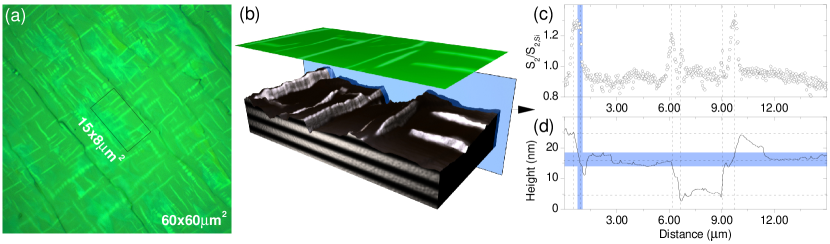
The commercial s-SNOM near-field microscope uses an illuminated AFM probing tip to scan the sample surface and pseudo-heterodyne interferometric detection Ocelic_Pseudohet_detection to extract the near-field amplitude and phase from the light scattered back from the tip. Standard platinum-coated AFM tips (NanoWorld ARROW-NCPt with a radius) were used as antennas for nanofocusing of laser radiation at () wavelength (photon energy). The measurements were carried out on optimally-doped superconducting RFS single crystals (batch BR26 in Ref. PhysRevB.84.144520, , ), cleaved prior to every scan. The sample surface was first characterized with a polarizing microscope. Figure 1(a) shows a patch of the sample surface. A network of bright stripes is always observed on a freshly cleaved surface and does not depend on the polarization of the probing light. The stripes always occur at with respect to the in-plane crystallographic axes. The topography of a representative surface patch studied with an s-SNOM microscope is shown in Fig. 1(b) as a three-dimensional terrain image. One can clearly correlate the features in the AFM map with the bright stripes in the polarizing microscope image. This implies that the surface chemistry of this compound leads to inherent surface termination with mesoscopic terracing upon cleaving, typically high. Figures 1(c) and 1(d) show the 2nd-harmonic near-field optical contrast (OC), obtained by normalizing the signal from the RFS surface to that that from a reference silicon surface (), and the topography profile of RFS for the cross-section indicated with a blue translucent plane in Fig. 1(b). The amplitude and phase of both the topography and the optical signal are obtained simultaneously during a scan. Every peak in the OC maps signals a metallic optical response. The absolute values of the complex dielectric function were obtained within the extended finite-dipole model Cvitkovic_07 using OC maps. The dielectric response of the semiconducting phase [dark regions in Fig. 1(b) and low OC in Fig. 1(c)] obtained in such a treatment of the experimental data () is fully consistent with that of the single-phase semiconducting RFS crystals 2011arXiv1108.5698C . The bright regions of the sample surface display negative values of , which provides solid evidence for their metallic character.
By correlating the OC peak positions with the topography maps one can deduce that the location of the metallic regions on the sample surface is bound to the slopes in the terrain, as indicated in Figs. 1(c) and 1d with dashed lines. Flat regions of the sample surface exhibit no metallic regions. Figure 1(d) shows that from the location of the OC peaks on the slopes one can identify well-defined sheets (horizontal dashed lines) approximately apart. Metallic response (OC peak) is recorded whenever one of these sheets is exposed from the sample bulk at the intersections of the dashed lines with the topography line. Such correlation exists in all studied cross-sections of the OC and height maps. The thickness of the metallic sheets can be estimated by projecting the full width at half maximum (FWHM) of the OC peaks onto the surface topography [blue shaded areas in Fig. 1(c) and 1(d)] and on average amounts to . The analysis of the correlations between the OC peaks and the slopes in the sample topography carried out on multiple cross-sections of different near-field maps shows that the metallic sheets have an in-plane dimension as well, which can be roughly estimated to in both directions. Therefore, phase separation in superconducting RFS single crystals occurs on the nanoscale in the out-of-plane and mesoscale in the in-plane direction. From the thickness and periodicity of the metallic sheets we can estimate the volume fraction of the metallic domains in the surface layer to approximately , significantly larger than all previously reported bulk values.
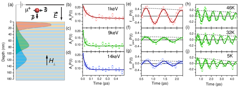
It must be noted that the metallic volume fraction obtained by means of s-SNOM imaging only considers the near surface layer within . Whether or not this fraction changes with the distance from the sample surface and what the magnetic and superconducting properties of the metallic and semiconducting phases are cannot be determined from these measurements. Therefore, a microscopic sensor of the local magnetic moment with an adjustable implantation depth must be invoked. Such characteristics are provided by the LE-SR technique, which utilizes the predominantly spin-oriented positron decay of to detect the orientation of the muon spin. This orientation is influenced by the local magnetic field at the muon implantation site, as well as magnetic fields applied externally. The experiment is shown schematically in Fig. 2(a). Based on the results of the near-field measurements the sample is sketched as an idealized periodic layered structure, the finite in-plane dimension of the paramagnetic domains and the irregularity of their periodicity having been disregarded at this point.
In the LE-SR technique, in contrast to its conventional counterpart, the incident energetic () muon beam is first moderated to about in a condensed layer of solid or Ar and then accelerated by a controlled electric field to achieve an adjustable implantation depth according to the muon stopping profile in a given material, calculated using the Monte Carlo algorithm TRIM.SP Morenzoni_stopping_profile_2002 . To study the dependence of the phase separation in RFS single crystals on the distance from the sample surface, we chose three muon stopping profiles shown as a red (achieved by accelerating the moderated muon beam to the energy of ), green (), and blue () shaded profile in Fig. 2(a). The resulting time dependence of spin polarization at zero external magnetic field is shown in Figs. 2(b)-(d), the colors correspond to those of the muon stopping profiles in Fig. 2(a). As is clear from Fig. 2(a), the shallowest muon stopping profile (red shaded area) is peaked at about and extends to about below the sample surface. It thus probes a region of the sample bulk comparable to that observed via s-SNOM. The relaxation of the muon polarization after implantation in the sample occurs at two different time scales: fast depolarization takes place during the first and is associated with the ordered antiferromagnetic phase, while a much slower evolution dominates thereafter and stems predominantly from the paramagnetic volume fraction. The fast depolarization rate is proportional to the width of the magnetic-field distribution at the muon stopping site in the ordered phase and thus to the antiferromagnetic moment. Figures 2(c) and 2(d) show that in the bulk [green and blue muon stopping profiles in Fig. 2(a)] the fast component is approximately the same and rather narrow, whereas near the surface it broadens significantly [Fig. 2(b)]. Using a two-component fit model for the zero-field SR data, the fast depolarization rates in the bulk were found to agree within the error bars: and for the green and blue profiles, respectively, whereas it is significantly reduced to close to the surface (red profile). Under the assumption that the muon stopping sites in the unit cell are the same for all three profiles and that the depolarization rate should be the same in the bulk, the antiferromagnetic moment is reduced to only of its bulk value in the surface layer.
The muon decay asymmetry in Figs. 2(b)-(d) indicates that the paramagnetic volume fraction (slow component) is enhanced closer to the surface. To avoid the contaminating SR signal originating from muon decays in the Ni sample holder, we carried out transverse-field measurements in the same configuration and at the same temperature of as in Figs. 2(b)-(d). In this case the oscillating component of the muon decay asymmetry comes only from the paramagnetic domains in the sample and can be normalized accordingly to become , where is the paramagnetic volume fraction, given by the value of the slowly depolarizing envelope of the muon spin precession (gray dashed lines in Fig. 2) at zero time. From Figs. 2(f) and 2(g) one immediately infers that well in the sample bulk the paramagnetic phase constitutes about of the sample volume. It thus characterizes the phase separation in the bulk of the superconducting RFS single crystals as probed by other techniques, such as Mössbauer spectroscopy and conventional SR. On the other hand, Fig. 2(e) shows that in the surface layer [red stopping profile in Fig. 2(a)] the paramagnetic volume fraction strongly increases to . Such a high value most likely occurs due to a reduced constraining potential between antiferromagnetic sheets with a significantly smaller ordered moment close to the sample surface, which leads to an expansion of the metallic regions. These depth-dependent physical properties could explain the difference in the chemical potential required for a consistent interpretation of the data obtained with bulk (inelastic neutron scattering) and surface-sensitive (ARPES) probes.
To characterize the superconducting phase of RFS with SR we studied the temperature dependence of the oscillating component of the muon asymmetry in a vortex state generated by the transverse external magnetic field, perpendicular to the metallic sheets. The oscillations are damped by the inhomogeneity of the magnetic field in the vortices, which, in turn, is proportional to the condensate density . The measurements were carried out in a transverse magnetic field for the muon stopping profile peaked at below the sample surface [green shaded area in Fig. 2(a)]. The time dependence of the normalized spin polarization in the normal state at and and in the superconducting state at is shown in Figs. 2(h)-(j), respectively. It is evident from the data that the damping in the normal state is approximately constant, while in the superconducting state it is noticeably faster, which indicates the presence of a superconducting condensate. By subtracting the normal-state damping from that in the superconducting state we can estimate the London penetration depth . Assuming that the phase separation in the bulk has the same layered structure as detected near the surface, this value must be revisited in an appropriate model. For a stack of superconducting layers of thickness separated by insulating layers of thickness the inhomogeneity of the magnetic field in a vortex (which is then a stack of two-dimensional vortex pancakes) is described by the Lawrence-Doniach in-plane penetration depth , related to the bulk London penetration depth via (see Ref. PhysRevB.43.7837, ). This reduction reflects the fact that is related to the average superconducting condensate density . Taking these considerations into account and using the bulk paramagnetic volume fraction obtained in our LE-SR measurements one can estimate the intrinsic bulk in-plane London penetration depth of the superconducting phase to be . This value would increase towards due to the finite in-plane dimension of the superconducting layers and their disordered stacking since the superconducting phase inclusions would then contribute independently to the SR depolarization. At the same time, our procedure slightly overestimates the value of due to the widening of the vortex field distribution close to the surface PhysRevLett.83.3932 .
Similar effective-medium approximations (EMA) must be used for an adequate analysis of the results obtained with other experimental techniques. A recent study of the optical conductivity of the same superconducting single crystals 2011arXiv1108.5698C emphasized the importance of EMA but could not make a concrete estimate due to the unknown details of the phase separation in this compound. It reported the total plasma frequency of the itinerant charge carriers of about . Using the same dimensions for the metallic paramagnetic and semiconducting antiferromagnetic layers as in the interpretation of the LE-SR results one can extract the bulk superconducting optical response from the conductivity data reported in Ref. 2011arXiv1108.5698C, . A simple fit of the experimental data as the optical response of a perfect superlattice gives a significantly larger value of the total plasma frequency and brings the estimated value of the London penetration depth closer to that obtained with LE-SR but still 8 times larger. Accounting for the finite in-plane dimension of the paramagnetic domains is expected to lead to a better agreement between the two techniques.
The origin of the phase separation observed in this work can lie either in a chemical stratification into e.g. iron-vacancy ordered (antiferromagnetic) and disordered (paramagnetic) phases or in a purely electronic segregation on a homogeneous crystalline background. Self-organization of a chemically homogeneous structure into (quasi)periodically segregated phases is not unprecedented — a similar phenomenon has been observed in copper-based superconductors, where antiferromagnetic stripes of copper spins were found to be spatially separated by periodic domain walls close to a particular hole doping level of Tranquada_Uchida_stripe_domains_1995 . Be it of chemical or electronic nature, the phase separation in superconducting RFS single crystals reported here represents an interesting case of a naturally-occurring quasi-heterostructure.
To conclude, by combining the unique optical imaging capabilities and nanoscale resolution of the s-SNOM near-field microscope with bulk sensitivity at variable depth of LE-SR we determined the geometry and magnitude of the phase separation in RFS superconducting single crystals. The paramagnetic domains were found to have a shape of thin metallic sheets parallel to the iron-selenide plane of the crystal with a characteristic size of only several nanometers out of plane but up to 10 m in plane. By means of LE-SR we further show that the antiferromagnetic semiconducting phase occupies of the sample volume in the bulk and is strongly weakened near the surface. These results have important implications for the interpretation of bulk- and surface-sensitive measurements on , and for the understanding of the interplay between superconductivity and antiferromagnetism in this material.
References
- (1) J. Guo et al., Phys. Rev. B 82, 180520 (2010).
- (2) J. J. Ying et al., Phys. Rev. B 83, 212502 (2011).
- (3) Y. Mizuguchi et al., Appl. Phys. Lett. 98, 042511 (2011).
- (4) A. F. Wang et al., Phys. Rev. B 83, 060512 (2011).
- (5) Y. Zhang et al., Nature Mater. 10, 273–277 (2011).
- (6) W. Bao et al., Chinese Phys. Lett. 28, 086104 (2011).
- (7) A. Ricci et al., Phys. Rev. B 84, 060511 (2011).
- (8) F. Chen et al., Phys. Rev. X 1, 021020 (2011).
- (9) R. H. Yuan et al., Sci. Rep. 2, 221 (2012).
- (10) A. Charnukha et al., arXiv:1108.5698 (unpublished) (2011).
- (11) V. Ksenofontov et al., Phys. Rev. B 84, 180508 (2011).
- (12) W. Li et al., Nature Phys. 8, 126–130 (2012).
- (13) M. Wang et al., Phys. Rev. B 84, 094504 (2011).
- (14) J. T. Park et al., Phys. Rev. Lett. 102, 117006 (2009).
- (15) D. S. Inosov et al., Phys. Rev. B 79, 224503 (2009).
- (16) P. Marsik et al., Phys. Rev. Lett. 105, 057001 (2010).
- (17) F. Ye et al., Phys. Rev. Lett. 107, 137003 (2011).
- (18) V. Ksenofontov et al., arXiv:1112.3822 (unpublished) (2011).
- (19) Z. Shermadini et al., arXiv:1111.5142 (unpublished) (2011).
- (20) Z. Wang et al., Phys. Rev. B 83, 140505 (2011).
- (21) G. Friemel et al., arXiv:1112.1636 (unpublished) (2011).
- (22) T. A. Maier et al., Phys. Rev. B 83, 100515 (2011).
- (23) R. Hillenbrand, T. Taubner and F. Keilmann, Nature 418, 159–162 (2002).
- (24) F. Keilmann and R. Hillenbrand, Nano-Optics and Near-Field Optical Microscopy (Artech House, 2008).
- (25) F. Huth et al., Nature Mater. 10, 352–356 (2011).
- (26) T. Prokscha et al., Nucl. Instrum. Methods Phys. Res., Sect. A 595, 317–331 (2008).
- (27) A. V. Boris et al., Science 332, 937–940 (2011).
- (28) N. Ocelic, A. Huber and R. Hillenbrand, Appl. Phys. Lett. 89, 101124 (2006).
- (29) V. Tsurkan et al., Phys. Rev. B 84, 144520 (2011).
- (30) A. Cvitkovic, N. Ocelic and R. Hillenbrand, Opt. Express 15, 8550–8565 (2007).
- (31) E. Morenzoni et al., Nucl. Instrum. Methods Phys. Res. B 192, 254–266 (2002).
- (32) J. R. Clem, Phys. Rev. B 43, 7837–7846 (1991).
- (33) C. Niedermayer et al., Phys. Rev. Lett. 83, 3932 (1999).
- (34) J. M. Tranquada et al., Nature 375, 561–563 (1995).