Observation of lattice thermal waves by the Blinking in photoluminescence of InGaN Quantum Well devices
Abstract
The photoluminescence of III-V wide band-gap semiconductors as InGaN is characterized by local intensity fluctuations, known as ’blinking points’, that despite decades of research are not yet completely understood. In this letter we report experimental data and a theoretical interpretation that suggests they are caused by the interference of thermal vibrations of the Quantum Well lattice. With far-field optical tests we could observe the lower frequency tail of these interference waves and study their dynamics as they propagate up to distances of several tens of microns.
I Introduction
The phenomenon called ’photoluminescence blinking’ have been observed in confined structures, as for example in semiconductors nanocrystals Nirmal et al. (1996). Because of the local nature of these systems, the theoretical treatment can be zero-dimensional (considering only time-energy dependence in one point). The blinking process results to be related to temporary quenching of photoluminescence due to highly efficient non-radiative recombination processes as for example Auger effect or other non-radiative processesBrosseau et al. (2010). Nevertheless, in InGaN devices the band structure is an infinitely wide quantum well, so a zero-dimensional model is insufficient, the understanding of the blinking phenomenon remains elusive Micheletto et al. (2009); Stefani et al. (2009); Micheletto et al. (2006); Kawakami et al. (2003).
In this letter we present experimental data and a wave model interpretation that suggests that the discussed optical fluctuations are a general phenomena caused by the interference of thermal vibrational waves that spread along the Quantum Well. Vibration alters the overlap integral, strongly displaced by piezoelectric fields in InxGa(1-x)N materials, and this affects the recombination rate inducing photoluminescence (PL) blinking. This idea is maybe difficult to grasp because thermally induced vibrations are supposed to be incoherent and of very high frequency, whereas PL blinking looks like a slow phenomenon that shows some sort of regularity.
However, in confined regions, atomic composition and mechanical properties are indeed homogeneous, giving rise to THz range vibrations with limited frequency spread and a certain degree of coherence. In correspondence of dislocations or impurities, mechanical properties of adjacent domains differ slightly, and vibrational interferences are generated. These interferences, simply called beats, have a broad frequency distribution centred around the frequency difference of the interacting oscillations. The lower frequency tail of this interference pattern is what it is observable as photoluminescence blinking.
We could confirm the thermal nature of the phenomenon with low temperature investigations. Moreover, using a simple far field correlation methodology we could observe the propagation and spread of PL beats along the quantum well area up to distances of several tens of microns.
II Theoretical insights
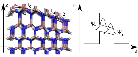
In a Quantum Well structured semiconductor as InxGa(1-x)N , the photoluminescence intensity is regulated by the matrix element that mediate the electron-density and hole-density wave function in the vicinity of the well Chuang and Chang (1996a, b). The spatial overlap of these two function is proportional to the recombination rate, and the latter results in more intense or weaker observable photoluminescence. The difference of inter-atomic distances (lattice mismatch) between the doped and non-doped regions causes piezo-electric stresses that distort the energy bands. This is resulting in diminished wave functions overlap and lower recombination rates due to quantum confined stark effect (QCSE)Rice et al. (2004); Das et al. (2011).
The Wurtzite InGaN quatum well is treated as a two-dimensional system subject to a stress along the direction ; because of spontaneous thermal vibrationJian et al. (2008), this stress is subject to very small oscillations that alters energy band structure (see the sketch in fig. 1).
The tension exerted on the line of adjacent atoms is indicated by , is a direction in the plane of the Quantum Well and is the crystal growth vertical axis. We are interested only in displacements along that are those that influence the matrix elements relative to the recombination rate. We derive the expression for the forces projected over the axis
| (1) |
where is a small displacement along the well, is the vertical displacement about the rest position and is a parameter proportional to the local linear mass density. This approach leads to the general differential expression of a wave oscillating along the crystal growth axis.
| (2) |
For generality frictional () and restoring () parameters are also included. In this classical approximation, we can say that influence of far away atoms is dumped by friction, hence the local solution is a wave of the form , where is related to and by .
Elastic mechanical oscillations can interact quasi-coherently in the confined scales, with the term quasi-coherent we mean that the waves have phase relation in confined ranges, but this relation is lost over longer distances.
Since the phenomenon is driven by spontaneous forces, frequencies are in the order of 1000 cm-1 (about 10THz) as shown in Raman studies and related literature Gotz et al. (1996); Deguchi et al. (1999); Micheletto et al. (2004); Kurimoto et al. (2001). Nevertheless, the observed blinking has components at few seconds rangeMicheletto et al. (2006). One may ask: how it is possible that the observed slow optical oscillations are induced by such higher frequencies? To answer this, we have to consider that vibrations are localized in a real, non-ideal, crystal system with different Indium concentration, dislocations and impurities that alter the overall vibrational modes.
In a classic interpretation, this implies that the frequency of oscillation , is in reality a spectrum of distributed values that depends on coordinates on the crystal plane . The mechanical interference of different distributed frequencies results in a wide band of lower frequencies beatings. The beating will be centred aroung , where and are the center frequencies of the vibration spectrum relative to two putative adjacent domains. Since mass distribution changes are subtle, can have tails extremely small compared to the original pulsation .
We observe optical fluctuations of about 10 20 at maximum, experimentation on InxGa(1-x)N devices shows that the quantum well thickness dependence on the intrinsic radiative lifetime is of about 1 order of magnitude per nanometer Berkowicz et al. (1999); Bai et al. (2000). Supposing that the PL oscillation are solely due to this phenomenon, then the greatest spatial displacement along the growth direction is in the range of 0.1 nanometers, a value compatible with the GaN crystal structure.
Thermal behaviour
To prove the mechanical nature of the blinking we study its dependence with temperature. We assume a Boltzmann statistic for the thermal oscillations and we want to verify if the observed photo-luminescence follows the same statistic with temperature.
In a solid we use as potential energy the expression , where is the Young modulus, the surface involved in the oscillation, its rest position and the displacement from it. Assuming a Boltzmann distribution , fixing a displacement one tenth of the maximum calculated above, nanometer and using InGaN Young modulus of 350 GPaJian et al. (2006), we can derive the potential dependence in a range of temperatures used in the tests (table 1 and figure 2).
| T | |||
|---|---|---|---|
| (∘ K) | (a.u.) | (a.u.) | (a.u.) |
| 200 | 1.99 | 1.54 | 0.44 |
| 230 | 4.49 | 3.6 | 0.88 |
| 250 | 6.92 | 5.65 | 1.27 |
| 270 | 10.0 | 8.29 | 1.71 |
| 280 | 11.7 | 9.83 | 1.95 |
| 290 | 13.7 | 11.5 | 2.20 |
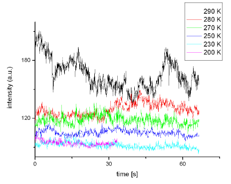
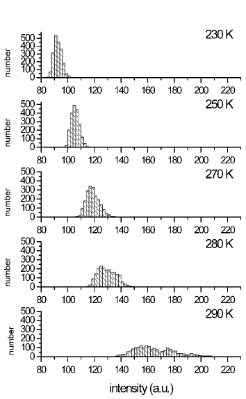
This expected behaviour was confirmed very straightforward tests. A vacuum low temperature chamber was used to observe the blinking at different temperatures ranging from down to Kelvin. For lower temperatures not only the average luminosity slightly reduces, but also the variations become less prominent (less blinking) accordingly to thermal model. In figure 2 the raw data are plotted against time, Figure 3 shows the luminosity distribution histograms at various temperatures. The spread and reduced luminosity of the blinking points predicted is evident.
Observation of propagating waves
We were able to directly detect the horizontal propagation of these interference waves alongside the quantum well. A CCD camera was mounted on a Olympus BX51-W1 microscope to record the photoluminescence on a wide area of the sample. Firstly, we choose a dominant blinking ”target” point in the recorded area, then we analysed the time-correlation of every other pixel to this point. The analysis was done in a time span of 120 seconds. In figure 4 we show the correlation coefficient map referred to a blinking point located at (10,30). The map in panel A show that regions adjacent to the target have an optical dynamics that is correlated to that point, whereas far away points have a more independent dynamics. This behaviour is expected.
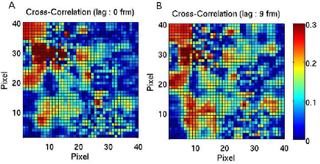
However, when we increase the time lag in the correlation analysis, we observe that as the correlation diminishes in the vicinity of the target as expected, also regions relatively distant from the center of blinking appear to increase in correlation. If we proceed to increase the lag shift, areas of increased correlation expand further, see area around (10,10) in fig. 4 panel B. This behaviour reveals how the expansion of mechanical beats located on the target are diffusing away from it. The structure and granularity of the correlation coefficient map, shows changing mechanical and mechanical properties along the lattices.
Conclusions
We have realized a simple model and experimental tests that suggest that the optical instabilities in InGaN quantum wells are caused by mechanical beats of thermal vibrations associated with the quantum well lattice. These beats have been observed experimentally through monitoring with CCD camera the photoluminescence and making a time resolved correlation analysis. Furthermore the thermal dependence of the phenomena is compared with a Boltzmann distribution of an harmonic oscillating lattice, resulting in good match and agreement with the original hypothesis.
We believe that the understanding of the thermal nature of the optical blinking in these devices is important not only for the understanding of the fundamental phenomena involved in the emission of InGaN materials, but also it can be the basis for a new general methodology of analysis of InGaN subtle local mechanical properties, revealing with a very simple and pure optical method, extremely small variation of doping concentration and possibly other fine compositional or structural perturbation in the crystal structure.
References
- Nirmal et al. (1996) M. Nirmal, B. O. Dabbousi, M. G. Bawendi, J. J. Macklin, J. K. Trautman, T. D. Harris, and L. E. Brus, Nature 383, 802 (1996).
- Brosseau et al. (2010) C. Brosseau, M. Perrin, C. Silva, and R. Leonelli, Phys. Rev. B 82, 085305 (2010).
- Micheletto et al. (2009) R. Micheletto, M. Allegrini, and Y. Kawakami, Applied Physics Letter 95, 211904 (2009).
- Stefani et al. (2009) F. Stefani, J. Hoogenboom, and E. Barkai, Phys. Today 62, 34 (2009).
- Micheletto et al. (2006) R. Micheletto, M. Abiko, A. Kaneta, Y. Kawakami, Y. Narukawa, and T. Mukai, Applied Physics Letters 88, 061118 (2006).
- Kawakami et al. (2003) Y. Kawakami, A. Kaneta, K. Omae, A. Shikanai, K. Okamoto, G. Marutsuki, Y. Narukawa, T. Mukai, and S. Fujita, physica status solidi (b) 240, 337 (2003).
- Chuang and Chang (1996a) S. Chuang and C. Chang, Physical Review B 54, 2491 (1996a).
- Chuang and Chang (1996b) S. Chuang and C. Chang, Applied Physics Letters 66, 1657 (1996b).
- Rice et al. (2004) J. H. Rice, J. W. Robinson, A. Jarjour, R. A. Taylor, R. A. Oliver, G. Briggs, A. D., M. J. Kappers, and C. J. Humphreys, Applied Physics Letters 84, 4110 (2004).
- Das et al. (2011) A. Das, G. P. Dimitrakopulos, Y. Kotsar, A. Lotsari, T. Kehagias, P. Komninou, and E. Monroy, Applied Physics Letters 98, 201911 (2011).
- Jian et al. (2008) S.-R. Jian, J. S.-C. Jang, Y.-S. Lai, P.-F. Yang, C.-S. Yang, H.-C. Wen, and C.-H. Tsai, Materials Chemistry and Physics 109, 360 (2008).
- Gotz et al. (1996) E. Gotz, N. M. Johnson, D. P. Bour, M. D. McCluskey, and E. E. Haller, Applied Physics Letters 69, 3725 (1996).
- Deguchi et al. (1999) T. Deguchi, D. Ichiryu, K. Toshikawa, k. Sekiguchi, T. Sota, R. Matsuo, T. Azuhata, M. Yamaguchi, T. Yagi, S. Chichibu, and S. Nakamura, Journal of Applied Physics 86, 1860 (1999).
- Micheletto et al. (2004) R. Micheletto, N. Yoshimatsu, A. Kaneta, Y. Kawakami, and S. Fujita, Applied Surface Science 229, 338 (2004).
- Kurimoto et al. (2001) E. Kurimoto, M. Takahashi, H. Harima, H. Mouri, K. Furukawa, M. Ishida, and T. M., Physica Status Solidi (b) 1, 103 (2001).
- Berkowicz et al. (1999) E. Berkowicz, D. Gershoni, G. Bahir, A. C. Abare, S. P. DenBaars, and L. A. Coldren, Physica Status Solidi (b) 216, 291 (1999).
- Bai et al. (2000) J. Bai, T. Wang, and S. Sakai, Journal of Applied Physics 88, 4729 (2000).
- Jian et al. (2006) S.-R. Jian, T.-H. Fang, and D.-S. Chuu, Applied Surface Science 252, 3033 (2006).