Dynamics of superconducting nanowires shunted with an external resistor
Abstract
We present the first study of superconducting nanowires shunted with an external resistor, geared towards understanding and controlling coherence and dissipation in nanowires. The dynamics is probed by measuring the evolution of the - characteristics and the distributions of switching and retrapping currents upon varying the shunt resistor and temperature. Theoretical analysis of the experiments indicates that as the value of the shunt resistance is decreased, the dynamics turns more coherent presumably due to stabilization of phase-slip centers in the wire and furthermore the switching current approaches the Bardeen’s prediction for equilibrium depairing current. By a detailed comparison between theory and experimental, we make headway into identifying regimes in which the quasi-one-dimensional wire can effectively be described by a zero-dimensional circuit model analogous to the RCSJ (resistively and capacitively shunted Josephson junction) model of Stewart and McCumber. Besides its fundamental significance, our study has implications for a range of promising technological applications.
pacs:
74.78.Na, 74.25.Fy, 74.25.Sv, 74.40.+k, 74.50.+rI Introduction
The dissipation of the supercurrent in thin superconducting wires occurs solely due to Little’s phase slips Little67 . Advances in fabricating ultra-narrow superconducting nanowires has greatly boosted the interest in studying phase slippage in quasi-one-dimensional superconductors Bezryadin08 . There has been an intense activity to establish the existence of quantum phase slips (QPS) related to macroscopic quantum tunneling (MQT) Gio90 ; Bezryadin00 ; Golubev01 ; Lau01 ; Tian05 ; Alt06 ; Zgirski08 ; Sahu09 ; LiWBBFC11 and to study quantum phase transitions between possibly superconducting, metallic and insulating phases in nanowiresBezryadin00 ; Lopatin05 ; Shah07 ; Refael07 ; DelMaestro08a ; DelMaestro08b ; Bollinger08 . A dissipation-controlled quantum phase transition Schmid83 ; Bulgadaev84 ; Chakravarty82 ; Zaikin97 ; Penttila99 ; Buchler04 ; Werner05 ; Meidan07 has been predicted in junctions of superconducting nanowires. Recently the importance of taking into account Joule-heating caused by dissipative phase-slip fluctuations has also been argued and demonstrated both theoretically and experimentally Tinkham03 ; Shah08 ; Sahu09 ; Pekker09 ; LiWBBFC11 . Furthermore, quantum theory shows that the QPS rate as well as the quantum phase transition can be controlled by an external shunt Buchler04 . Dissipation plays an important role in dictating the physics of nanowires. Conversely, superconducting nanowires provide an ideal prototype for studying the interplay between coherence, dissipation and fluctuations. Besides their fundamental importance, superconducting nanowires are also ideally suited for building superconducting nano-circuitry and as devices with potentially important applications, such as superconducting qubits and current standards Mooij05 ; Mooij06 . Thus, even from the technological point of view, it is extremely important to fundamentally understand the mechanism and role of dissipation in nanowires and to find a way of experimentally controlling coherence and dissipation.
It is well established that the environmental dissipation of Josephson junction (JJ) can be controlled by externally shunting the junction Tinkham96 . This effect has been observed in the voltage-current - characteristics, which are greatly altered by the amount of dissipation. The statistics of the switching and retrapping behavior in shunted JJs have been investigated in last three decades and continues to be actively studied BenJacob82 ; Martinis89 ; Vion96 ; Kivioja05 ; Krasnov07 ; Mannik05 ; Krasnov05 ; Myung09 . In general, the retrapping current, which is inversely proportional to the quality factor of the circuit, is more sensitive to the amount of damping/dissipation than the switching current. The shunting is also known to control the rate of MQT of the phase variable in superconductor-insulator-superconductor (SIS) junctions Takaqi05 ; Leggett78 ; Leggett86 ; Caldeira81 ; Leggett87 ; Voss81 ; Martinis87 ; Martinis88 . The Stewart-McCumber model Stewart68 ; McCumber68 of resistively and capacitively shunted Josephson junctions (RCSJs) accurately describes much of the physics of shunted JJs Tinkham96 ; Likharev81 . This model is quite useful since it allows the analysis of various fundamental aspects of superconducting devices, including chaotic behavior Khawaja08 and high-frequency microwave responses Naito84 . The analysis of superconducting computational circuits also involves use of the RCSJ model Dimov05 .
Shunting a superconducting nanowire with a normal resistor should have a strong effect on the superconducting character of the wire and just as in the case of JJ could potentially provide a powerful way to control coherence and dissipation. In spite of its clear importance and relevance, the behavior of shunted nanowires has not been studied previously both experimentally and theoretically. Here, we present the first study of shunted nanowires. It has been inarguably proven for the case of unshunted nanowires that going beyond linear response is essential to probe the dynamics of (quantum) phase-slip fluctuations Tinkham03 ; Shah08 ; Sahu09 ; Pekker09 ; LiWBBFC11 . Furthermore, most applications would require the wire to be driven out-of-equilibrium, making it doubly important to understand how the dynamics of shunted nanowires evolves upon shunting. In fact, there is a third equally important motivation for such a study. As discussed above, the RCSJ model has been successfully used for JJs and has proven to be extremely important. However, a circuit-element representation of a superconducting nanowire is currently lacking and through this work we want to fill this gap by making some concrete advances in that direction.
The nanowires on which measurements were performed in the present work were located in a low-pressure, thermalized helium gas and were fabricated using the molecular templating method resulting in suspended nanowires Bezryadin00 ; Bezryadin08 . It had already been demonstrated that these superconducting nanowire show a large hysteresis in the - characteristics for the unshunted case and that this hysteresis stems from Joule heating and the strong temperature dependence of the resistance of the wire Tinkham03 ; Shah08 ; Sahu09 ; Pekker09 . Local Joule heating by phase-slip processes is especially important for a long free-standing nanowire because the heat generated in the bulk of the wire is not removed easily and has to flow away through the ends of the wire. Observation of similar physics in a recent study of Aluminium nanowires fabricated using a different method LiWBBFC11 points to the ubiquity and importance of Joule heating effects and further underlines how it can be turned into an effective probe for quantum phase slips. However, the best case scenario will be to be able to have a control over the Joule heating. As will be shown in this paper heating can indeed be controlled by shunting the superconducting nanowire with an external resistance.
The article is organized as follows. In the next Sec. II we briefly describe the sample fabrication and measurement technique. The experimental results are presented in Sec. III. This is followed by our theoretical analysis and discussion in Sec. IV where we will argue that shunting qualitatively changes the behavior of the nanowire and present the theoretical results obtained by modelling the nanowire. Finally we will end with concluding remarks in Sec. V.
II Sample fabrication and measurement technique
The nanowires presented in this study are fabricated using molecular templating Bezryadin08 ; Bezryadin00 . Using electron-beam lithography and a reactive ion etch, a 100 nm wide trench is patterned in the SiN layer of a Si-SiO2-SiN substrate. The trench is then etched in a solution of hydrofluoric acid to form an undercut to prevent electrical leakage between the electrodes, which are separated by the trench Bezryadin97 . Fluorinated single-walled nanotubes, which are insulating, are dissolved in isopropanol and then deposited onto the substrate containing the 100 nm wide trench in the SiN layer and then dried with nitrogen gas. Randomly, some of the nanotubes cross the trench, creating a scaffold for the nanowires to form as the metal of choice is deposited on the substrate. The samples are then DC sputtered with amorphous Mo76Ge24 in a high vacuum ( Torr base pressure) chamber, thus coating the substrate and nanotubes with 12-18 nm of MoGe depending on the sample. A scanning electron microscope (SEM) is then used to image the trench until a MoGe coated nanotube (nanowire) is found to be relatively straight, homogeneous, and coplanar with the electrodes Bezryadin08 . An SEM image of one such nanowire is shown in the inset of Fig.2(a). Contact pads are formed using photo lithography and wet etching in a solution of H2O2, which etches MoGe rapidly.
All of the samples studied in this paper are 100 nm long and are fabricated using MoGe. The thickness of each nanowire is controlled by the deposition time in the sputtering chamber and by the configuration of nanotubes used as a scaffold. The actual width of each sample is measured from the SEM image and found to be 15, 12, 10, 15, 8, and 18 nm for samples S1, S2, S3, S4, S5, and S6 respectively. Thicker samples show a lower normal resistance , higher critical temperature , higher critical current , and slightly higher retrapping current . For example, for samples S1, S2 and S3 which have a decreasing thickness, the resistance in the normal state and critical temperature are S1 , S2 , and S3 . All samples visually show a similar behavior in the - and - curves.
The shunt has been added by attaching a commercial metal film resistor (ranging from 5 to 200 ) parallel to the sample using silver paste (Fig.1(b)). The distance from the nanowire to the shunt is 1-2 cm for all samples, and the shunt resistance is measured as a function of temperature down to cryogenic temperatures and found to be constant. Measurements are performed in a or cryostat equipped with base temperature silver paste and copper powder filters and room temperature -filters. Transport measurements are carried out by current biasing the sample through a large resistor (1 M) and measuring the voltage with a battery-operated Stanford SR 560 preamp, using the typical film-inclusive four-probe technique as in Fig.1(b) Bezryadin00 . Resistance vs. temperature (-) curves are measured by applying a small sinusoidal current (10-100 nA) at a frequency of 12 Hz and measuring the voltage and then doing a linear fit to the resulting voltage-current data to obtain the resistance. The temperature is measured using a calibrated Cernox thermometer from LakeShore. - curves are measured by applying a large sinusoidal current in the range of a few A, at a frequency of a few Hz, and measuring the voltage simultaneously. The switching (retrapping) current has been measured by sweeping the current as in the - measurement, and recording the current at which the voltage-jump (drop) out of the superconducting (resistive) state has been the greatest.
III Experimental results
In this section we present a series of experimental results. We begin by presenting the temperature dependence of the linear resistance of shunted nanowires and use that as a benchmark for characterizing different samples. Next, we go one step further and present the measurements of the nonlinear - characteristics of the current-biased nanowires at temperature of K, focusing on the evolution of hysteresis upon shunting. In the next subsection the experimental data of switching and retrapping distributions for different values of shunt are presented. Such an analysis provides deeper insights into the dynamics of superconducting nanowires as is evident from a previous study in the case of unshunted wiresShah08 ; Sahu09 ; Pekker09 . Although the focus of our work is on studying the effect of shunting, in the last subsection we present the temperature dependence of the - characteristics and the switching distributions so as to provide a comparison with the corresponding measurements for the unshunted case that was studied in detailShah08 ; Sahu09 ; Pekker09 .
III.1 Shunt dependence of : characterization of the samples
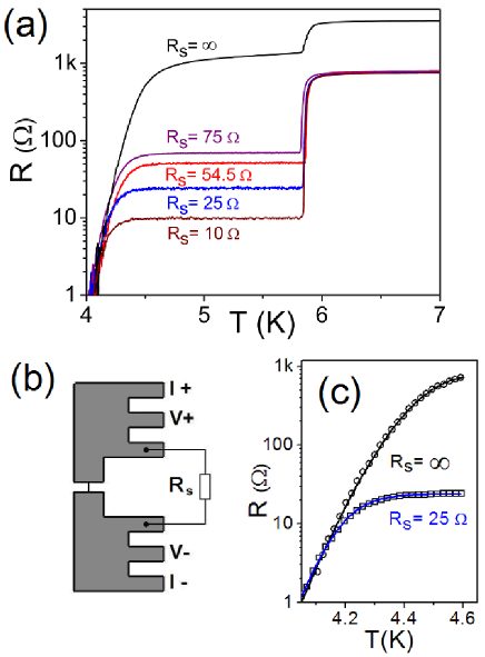
Study of the linear-response resistance as a function of temperature is useful for characterizing the samples and establishing a starting point for further investigation. Fig.1(a) shows the temperature dependence of the nanowire’s resistance using a log-linear scale for various values of the shunt resistance . As the temperature is lowered below 5.8 K the film becomes superconducting while the wire is still resistive because its critical temperature is lower than that of the film. Below of the wire, as expected there is a measurable resistance due to phase slips in the wire.
We understand the measured resistance vs. temperature - curves using the following arguments. Below of the nanowire the total sample resistance is a parallel combination of the and the wire resistance, . We model the wire resistance with an empirical formula,
| (1) |
where is the normal state resistance of the nanowire to account for the quasi-particle resistance channel and is the Arrhenius-Little (AL) resistance occurring due to thermally activated phase slips (TAPS). The AL resistance is estimated, following Little’s proposal, by assuming that each phase slip creates a normal segment on the wire of a size equal to the coherence length and for a time interval roughly equal to the inverse attempt frequency Little67 ; Bezryadin08 . We note that the Langer-Ambegaokar-McCumber-Halperin (LAMH) theory Langer67 ; McCumber70 of TAPS is not valid except very near to Meidan07 . So we have to use the phenomenological AL expression:
is the free energy barrier for a phase slip in the zero-bias regime Langer67 . Here is the thermodynamic critical field, is the temperature dependant coherence length, is the cross-sectional area of the wire, and is the Boltzmann constant. The equation for the free energy barrier can be rewritten to include wire parameters more accessible via the experiment as Tinkham02
| (2) |
where is the length of the nanowire and is the quantum resistance. Thus, the temperature-dependent total sample resistance is:
| (3) |
The fits of the total sample resistance by Eq.(3) are presented in Fig.1(c) for the unshunted nanowire , and the case when the nanowire is shunted with . All the fits are done by using the values of , , , and obtained from the - curve and the SEM image and using , and as fitting parameters. The value of the fitting parameters change very slightly as the shunt resistance is varied. For instance, in the fitting presented in Fig.1(c), the value of decreased by 12 mK for the shunted case compared to the unshunted case, which can be accounted for by slight sample change during thermal cycling. The agreement between experimentally measured resistance and the total resistance in Eq.(3), as shown in Fig.1(c), gives evidence that the -dependence of the rate of phase slips does not depend on the shunt at relatively high temperatures ( in this case) and that the observed residual resistance of the wire just below is due to TAPS in the high temperature limit of . Note also that the - curves of all the samples presented in this paper are smooth and show no extra transitions, and the SEM images confirm that the nanowires are homogeneous and well-connected to the electrodes. Thus our nanowires are well suited to systematically study the effect of shunting.
III.2 Shunt dependence of - characteristics
Let us start by considering the unshunted wire . As the bias current is increased, thermal fluctuations cause the nanowire to switch from a superconducting state into a resistive state before the current reaches the critical (equilibrium) depairing current. The current at which the wire switches out of the superconducting state is called the switching current . Once in the resistive state, as the current is decreased below some critical value of current, the nanowire experiences retrapping back into the superconducting state. The current at which this happens is called the retrapping current . For unshunted wires, switching is stochastic in nature, i.e., each new current sweep gives a different value for the switching current but the retrapping process is non-stochastic. We devote the next subsection for the discussion of switching and retrapping distributions and their dependence on the shunt resistance. Here we focus on the mean values of the switching and retrapping currents and show how they evolve upon shunting the wire as shown in Fig.2.
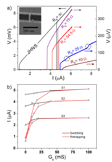
Fig.2(a) shows the - characteristics for different values of shunt resistance. As the nanowire is shunted with lower values of the shunt resistance, the mean switching and retrapping currents are increased while the width of the hysteresis is decreased. Additionally, the retrapping current also becomes stochastic (as shown in Fig.4). In Fig.2(b), the dependence of the mean switching and retrapping currents on the shunt resistance are shown for different nanowire samples. The mean switching current increases, at a lower rate than the retrapping current, and saturates for small values of the shunt resistance (Fig.2(b)) with a decreasing (increasing) shunt resistance (conductance . Similarly, the retrapping current increases with decreasing the shunt resistance until finally reaches of the wire. Such behavior is observed on all tested samples. As the switching and retrapping current coincide, the hysteresis disappears. Nanowires with smaller start showing this saturation behavior at higher shunt values.
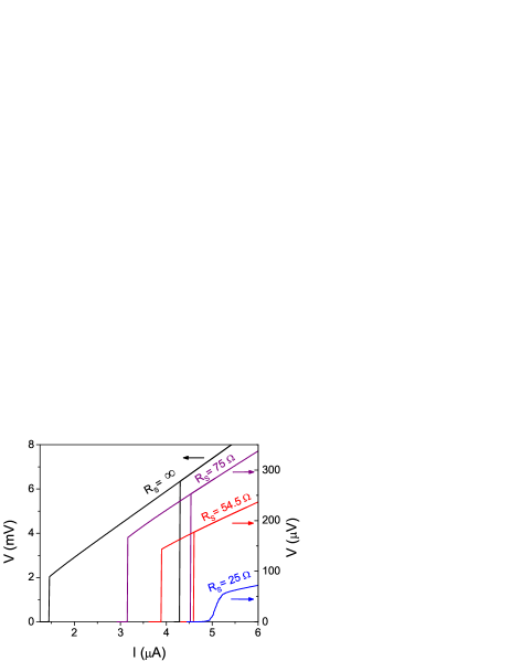
When the nanowire is shunted with a resistor or less, kinks in the voltage are also observed (they are marked by dashed line circles in Fig.2(a) for the case where sample S1 is shunted by . The kinks for the shunting case are not shown, but occur at higher current. We relegate the interpretation of these kinks to Subsec. IV.4.
III.3 Shunt dependence of switching and retrapping distributions
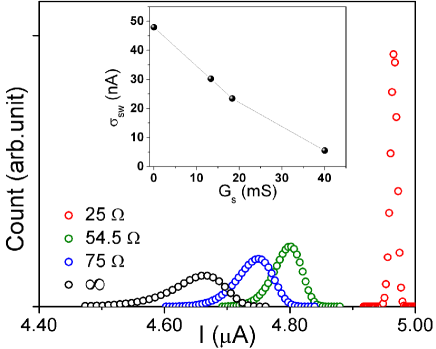
As mentioned in the previous subsection, the unshunted nanowire undergoes stochastic switching as the bias current is increased. We plot the switching distributions vs. current in Fig.3 for different values of external shunt resistance to see how it evolves upon shunting. Lowering the value of the shunt resistance has the effect of narrowing the width, increasing the height, and shifting the distribution to higher currents. As can be seen from the plots, the full width of the distribution at half maximum (FWHM) changed from 100 nA to 12 nA due to shunting with a resistor. The asymmetric shape in the distribution for larger shunts changes to a rather symmetric shape with lower shunts.
The retrapping current also shows a dramatic change from deterministic values to stochastic values when shunted with 75 or less. The bottom part of Fig.4 is a typical retrapping histogram for an unshunted wireSahu09 . Here, the standard deviation of the retrapping current is 1.51 nA, which is the noise limit of our experimental setup. So, this small distribution of retrapping current is just due to the instrumental noise, and can be reduced by decreasing the instrumental noise and the spacing in between bias-current points. Thus, retrapping in unshunted nanowire always occurs at the same current, i.e. the transition is deterministic. However, when the wire is externally shunted, a retrapping distribution is observed, with its width being much larger than the experimental setup noise and independent of the bias-current spacing.
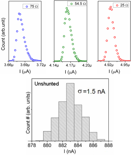
In the top of Fig.4, the retrapping current distributions for sample S1 are shown for the nanowire shunted with different values of external resistances. The width of the distribution is slightly sensitive to the value of shunt resistance, but the mean value of the retrapping current changes considerably. When shunted with for instance, the standard deviation of the retrapping current increases above the experimental setup noise to 7.3 nA (from 1.5 nA for the unshunted case under the same conditions). Interestingly the width of the retrapping and switching current distributions for 25 shunt is almost similar. The retrapping distributions for the shunted nanowire are asymmetric in contrast to the unshunted case in which the distribution is symmetric as can be seen in the bottom of Fig.4.
III.4 Temperature dependence: shunted vs. unshunted nanowires
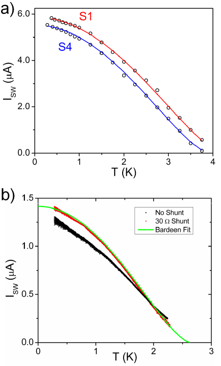
In this subsection we discuss the temperature evolution of the dynamics of shunted nanowires. In Fig.5(a), the mean value of the switching current is plotted at various temperatures for sample S1 shunted with and sample S4 shunted with . In Fig.5(b), a distribution of switching currents is plotted as a function of temperature for sample S5 when it is shunted with a resistor and compared with the unshunted case. As the temperature is reduced, the switching current for all samples increases and begins to show signs of saturation below K. The behavior of the switching current as a function of temperature in the distribution measurement in Fig.5(b) is similar to that of Fig.5(a) except that in Fig.5(b) the fluctuation in the switching current is also displayed.
To check the proximity of the switching current to the equilibrium depairing current, Bardeen’s prediction Bardeen62 for the temperature dependence of the equilibrium critical (depairing) current is compared to the temperature dependence of the measured switching current for nanowires shunted with small resistances as shown in Fig.5. The Bardeen’s equation, derived from BCS theory, is given by:
| (4) |
where is the critical current at zero temperature. Excellent agreement is found with the experimental data over a wide temperature interval suggesting that the shunt has driven the switching current close to the depairing current. In these fits, the temperature is known while the critical current at zero temperature and the critical temperature are used as fitting parameters. Close agreement is found between the theoretical prediction for the depairing current at zero temperature: Tinkham02 , which is derived from BCS and Ginzburg-Landau theory, and the value of used in the Bardeen fit. Here and are in nm, in K , and in . Using the fitting parameters from the fit of Eq.(3) presented in Fig.1(c), has a theoretical value of , while used in fitting to the Bardeen formula in Fig.5 has a value of . Thus, excellent agreement is found between the theoretical and experimental value for . A value of K for is used to fit the temperature dependence of the switching current with the Bardeen formula, while the fit using the AL model predicts the value of to be K. This difference can be accounted for by sample oxidation and thermal cycling between measurements.
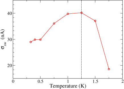
Finally in Fig.6, we plot the measured temperature dependence of the switching distribution width for the shunted nanowires. We find that it shows a trend similar to that previously observed for the unshunted wireSahu09 . As for the retrapping current, which is observed to be stochastic only in the shunted nanowire, the standard deviation is never observed to increase with decreasing temperature. However, at low temperatures, MQT is expected to cause the standard deviation of the retrapping current to be constant with temperature Chen88 . In our experiments, we have seen evidence of this behavior and will investigate this more fully in the future.
IV Theoretical analysis and discussion
In this section we will develop a theoretical interpretation and understanding of the experimental data presented in the previous section. In doing so, we will start by giving a brief account of the unshunted nanowires which have been previously investigated in detail. Then we will argue how shunting the nanowires brings about qualitative changes in the dynamics and develop a physical picture by gathering experimental signatures and theoretical arguments. Next we will motivate the theoretical model for explicit calculations and numerical simulations and use it to generate the - characteristics and the distributions that will be compared with experimental measurements.
IV.1 Unshunted nanowires
Recently, properties such as the - characteristics and the switching distributions of the unshunted nanowire have been studied in detail to understand the behavior of quasi-one-dimensional superconductors at low temperatures Shah08 ; Sahu09 ; Pekker09 ; LiWBBFC11 . In quasi-one-dimensional superconductors the zero resistance superconducting state is destabilized by thermal and quantum phase-slip fluctuations. These phase-slip fluctuations induce resistance which causes Joule heating in the nanowire. If this heat generated by phase-slip fluctuations in the bulk of the wire is not overcome sufficiently rapidly, it can reduce the depairing current to below the applied current, thus causing transition to the highly resistive state. It has been found in experiments with unshunted nanowire that while the distribution of re-trapping currents is very narrow and almost temperature-independent, the distribution of switching currents is relatively broad and the mean as well as the width of the distribution change with temperature of the leads. The distribution in switching currents reflects that the collective dynamics of the superconducting condensate evolves stochastically in time and undergoes phase slip events at random instants. A stochastic model for the time-evolution of the temperature in a nanowire has been developed to understand above experimental results Shah08 ; Pekker09 . The model predicts that although, in general, switching from superconducting to resistive normal state occurs due to several phase-slip events, it can be even induced by a single phase slip at a particular temperature and current-range. The model also indicates non-monotonic temperature dependence of the width of the distribution of switching currents. Thus, these experiments with switching events as well as those with microwave radiation in unshunted wires suggest that the resistive state is the normal state of the wire maintained by Joule heating, i.e. the JHNS Tinkham03 ; Sahu09 ; Dinsmore08 ; LiWBBFC11 . For unshunted wires, the retrapping process is non-stochastic since the retrapping occurs from the thermalized Joule heating state.
IV.2 Qualitative picture of shunt-induced crossover
How does the picture for the unshunted case discussed above evolve as we shunt the wire with an external resistance? With the inclusion of a shunt resistance the applied bias current is divided into two parts, and the part going through the nanowire decreases as the shunt resistance becomes smaller. A lower (higher) current through the wire causes a decrease (increase) in Joule heating in the wire and hence a decrease (increase) in local temperature. For the unshunted case that corresponds to an infinite shunt resistance, the heating is maximum and as discussed in the previous subsection one gets a JHNS in the unshunted wire.
We will argue that upon decreasing the value of the shunt resistance the nature of the resistive state of the nanowire changes from a JHNS to a phase slip center (PSC) state. PSC is a process of periodic-in-time phase rotation occurring in a certain region of the wire and is driven by the bias current. An ideal PSC acts qualitatively like a weak-link JJ in series with the rest of the wire, and the differential resistance associated with it is determined by the quasiparticle diffusion length Skocpol74 . This resistance is much smaller than the normal resistance of the wire. This is what we indeed obtain when the nanowires are shunted with small resistance. The most explicit proof for a PSC would of course be the observation of Shapiro steps, because they prove that there is a periodic phase rotation in the system. However we have compelling arguments and consistency in our explanation that points to the existence of PSC.
The deterministic retrapping current observed for the unshunted nanowires becomes stochastic when an external resistive shunt is added (at least within the experimental range of shunt resistances). The deterministic retrapping current reflects that the resistive state of the unshunted wires is a thermalized JHNS. There is overheating and the wire is normal. As is reduced the temperature goes down. Relative fluctuations of the temperature are small since it is determined by a macroscopic number of normal electrons. In this case is fixed by the current at which the heating is not enough to keep the system above . If the system must re-trap at then as can be seen in Fig.4, the distribution is symmetric and Gaussian, centered around , and as wide as the noise in the bias current circuit and in the measurement circuit can smear it. On the other hand, the stochastic retrapping current indicates that the finite-voltage/resistive state of the shunted wires is governed by a coherent dynamics of the phase of superconducting order parameter. The dynamic state, called PSC moves by inertia, which is the voltage on the electrodes. But a strong thermal (or quantum) fluctuation can re-trap the system from the dynamic to the static state. And such change will be permanent. So the retrapping can happen at . The distribution is asymmetric (right-skewed or right-tailed) since the system can never switch at . Here, the fluctuation-free retrapping current is the current value at which the friction must stop the dynamic state in all cases (this is the property of the model considered). Similarly, the fluctuations in the low-resistance ‘superconducting’ state as discussed in the previous subsection for the unshunted case can allow for premature switching at but never at since the system cannot move through without a switch (the bias current I is assumed to grow linearly in time). One again has an asymmetric distribution, this time left-skewed or left-tailed. Overall, we can use the shape of the distribution to gain insights into nature of the state from which retrapping or switching happens.
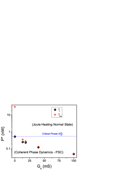
In Fig.7, a phase diagram for sample S1 is presented which demonstrates the conditions necessary for the resistive state to be either the JHNS or a coherent phase dynamics state such as a PSC. The power at switching and retrapping is calculated by taking the product of the current through the wire and voltage across the wire at which the system exhibits switching and retrapping, respectively. Here, , where is the total current, which obeys Kirchhoff’s Law for current conservation (, where is the current through the shunt). The critical power, , is defined as the minimum power the wire can sustain and still remain in the JHNS and is calculated from the power that the unshunted nanowire exhibits at retrapping. For sample S1, is calculated to be 0.533 nW from the unshunted curve in Fig.2(a). At switching, the unshunted wire experiences 31 nW of heating, which puts it in the JHNS, where it remains until the current is reduced below the retrapping current.
With an included shunt, the Joule heating power in the wire at switching is reduced. For example, when shunted with , the Joule heating power at switching is 0.359 nW (compared to 31 nW for the unshunted wire), which is lower than . Thus, the wire switches to the PSC, which is a superconducting dynamic state (and not the normal state), and as the current is reduced, it remains in it until retrapping occurs. Because retrapping occurs from the phase coherent state, stochastic retrapping is expected for sample S1 when shunted with (from the experimentally examined values) a resistor or less. Some heating is also to be expected since the power at retrapping is still comparable to .
Guided by the qualitative picture developed above, in the next subsection we will discuss a model that we will use for simulating the dynamics of the nanowire. In Subsec. IV.4 we will address the kinks seen in Fig.2(a) and argue that they further support the existence of a coherent phase dynamic state or a PSC for shunted nanowires.
IV.3 Theoretical model for shunted nanowires

As argued in the previous subsection, shunting changes the high-resistance state from JHNS to a state with coherent phase dynamics or PSC. When the value of the shunt resistance is small, we expect that the dynamics of the nanowire can be modelled by an effectively zero-dimensional circuit model as is done in the case of a JJ given that the PSC behaves like a JJ in series with the wire. For unshunted nanowires (i.e. infinite shunt value) heating is important and as discussed above the dynamics of the nanowire is dictated by a model stemming from a heat diffusion equation. For very large shunt values some elements of this model might still be important. However, the point of view we take is to simulate the dynamics of shunted nanowires using a circuit-element representation and see how well we can reproduce the experimentally observed behavior.
As discussed in the introduction, the RCSJ model of Stewart and McCumber has been greatly successful in understanding the physics of JJs. So our goal is to adopt and extend this model to reflect the experimental set-up and measurements for the nanowires considered in this paper. The model of Stewart and McCumber was originally introduced for superconducting JJs to study dc - curves displaying hysteresis for light damping Stewart68 ; McCumber68 . This model considered only the time varying phase difference of the superconducting wave-functions in the weakly coupled superconductors and neglected any spatial variations of the superconducting wave-functions and is essentially zero-dimensional. We add an external shunt resistance in parallel with the superconducting junction in the RCSJ model to be able to study the behavior for different values of external shunt resistance as has been studied experimentally. We then simulate the extended RCSJ model with the Johnson-Nyquist Gaussian white thermal noise coming from the resistive parts of the circuit. We have not included external noise in our simulation. Before presenting the details of the model, we pause to provide some examples of analogies of the observed nanowire behavior with the established behavior in JJ to further motivate the use of a RSCJ kind of model for the case of a shunted wire.
The hysteresis in underdamped JJs is due to the bistability of the phase point in the tilted wash-board potential which depends nonlinearly on the bias current Tinkham96 . Damping plays an important role in dictating the dynamics of the JJ. The experimentally observed saturation of at low shunt values as presented in Section. III can be interpreted to be an effect of high damping (damping on the premature switching process, and it indicates that the depairing current is nearly reached for these low values of the shunt. Another experimental observation we presented earlier is that below some critical shunt value, the retrapping and switching current become equal and the hysteresis vanishes. For instance, for sample S1 at 1.8 K at a shunt value of , the - curve becomes non-hysteretic as in Fig. 2(a), and there is no abrupt switch into the resistive state. This can be interpreted in analogy to JJ as follows: At some critical value of the shunt, the increased damping changes the system from an underdamped junction (with hysteresis) to an overdamped junction (without hysteresis). In JJs, this transition occurs when Krasnov07 . the third example of analogy with JJs is that the mean value of the retrapping current changes considerably upon changing the value of the shunt resistance. Indeed it is well-known for JJs that retrapping is very sensitive to the value of damping and the fluctuation free retrapping current is inversely proportional to the resistance associated with the JJ.
We give a brief summary of the physics of the RCSJ model in Appendix A and focus on discussing the details of our extended RCSJ model below. The displacement current and “normal” losses (e.g. quasiparticle tunnel currents) in the nanowire are included in the model by the shunting capacitance and resistance , respectively. We also include a Johnson-Nyquist type Gaussian white noise current source associated with the resistance along with the drive current source Ambegaokar69 ; Kurkijarvi70 . Next we extend the RCSJ model with an external normal resistance and corresponding Johnson-Nyquist Gaussian white current noise for the present experimental set-up of a shunted nanowire (see Fig.8). Then, the reduced equation of motion for the phase difference is given by (check Appendix A for a derivation)
| (5) |
where is the quality factor, is the normalized dc bias current, are the normalized noise currents, where is the physical time associated with the circuit in Fig.8. Here is the fluctuation-free critical current of the nanowire. The time-averaged steady-state voltage across the wire, , and the noise autocorrelations are
| (6) | ||||
| (7) |
where denotes averaging over the noise realizations (noise ensemble). The temperature of the nanowire and the shunt resistance are and , respectively. It is possible that the temperature of the wire is different from that of the shunt resistance, so we keep here two different noises coming from two different resistances. The relations in Eqs.(6,7) are known as fluctuation-dissipation relations. Now if we assume that there is not significant MQT at the temperature (1.8 K) where the distributions for the switching current and the retrapping current are measured, then the distributions are due to the thermal fluctuations arising from the Johnson-Nyquist current noises associated with the resistive parts of the circuit.
IV.4 Shunt dependence of - characteristics
Now we simulate Eq.(5) for to calculate the voltage-current characteristics of the shunted nanowire in the presence of the current noises from the normal resistances. In the experiment, one changes the bias current with a finite current sweep rate, and measures the corresponding voltages. In the simulation, instead we first fix a bias current and then integrate the above equations of motion (with suitable initial conditions and current noises) for a sufficiently long time (this time is the relaxation time or the transient time), and next calculate the time-averaged voltage by averaging over some time interval. For forward current sweep we choose the initial conditions, ,; and for the backward current sweep we use , . The initial values of and for the backward current sweep can be any finite non-zero values in the resistive state of the system as after long time of transient dynamics the exact initial values of and are irrelevant. We generate the Gaussian white noises and at each time step of the simulation satisfying the noise properties in Eqs.(6, 7) following the method described in Allen .
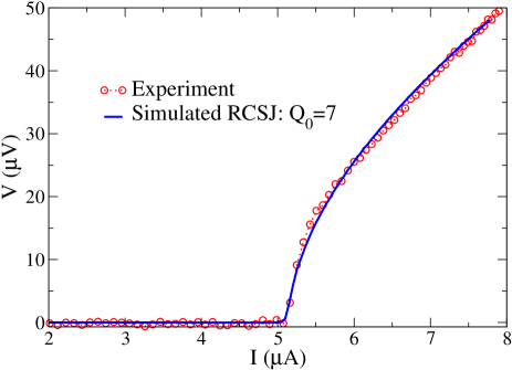
The voltage-current characteristics are plotted in Fig.9 for the shunted wires with different values of the normal resistance of the wire and the shunt resistance. As can be seen from the Eqs.(5,13), we really do not need explicit values of the resistances in simulation, but we only need the ratios of the two resistances and a quality factor. We have checked that for the quality factor and at a specific temperature K, the transition from hysteretic to non-hysteretic behavior occurs near the ratio . As discussed in the previous subsection, our present theory with a coherent phase relationship suits us best to analyze the nanowires shunted with low shunt resistance, i.e., in the PSC regime. A comparison between Fig.2(a) and Fig.9 shows a very good qualitative agreement between the experimental - curves and those from simulations. We also have good quantitative agreement between the experiment and simulation for the - curves of the shunted nanowires (PSC regime) with small resistances. This is shown in Fig.10 for the shunted nanowire case where . We find the best agreement between the experimental and simulated - curves for the low shunt resistances when the effective temperature (related to the thermal noise) of the simulated nanowires is much lower than the temperature of the superconducting electrodes in the experiment. Therefore the fluctuation in due to thermal noise is expected to be small as we find in experiment. The reason for such effective thermal noise reduction is not completely clear. It might be due to the inductance of the shunt resistance. The inductance can cut-off some of the higher-frequency thermal noise, thus reducing the standard deviation of the noise current. It also confirms that Joule heating in the shunted nanowires for lower shunt resistance is greatly reduced compared to the unshunted case. The resistance of the shunted nanowires which enters in the simulation through Eqs.5, 7 is used as a fitting parameter here. It is necessary to choose it to be much smaller than the normal resistance of the nanowire to have the best fitted of - curves. This is a strong indication that the shunt resistance drives the nanowire to a phase-coherent PSC state, in which the time-average supercurrent is not much smaller than the total bias current. Thus we introduce a new notation for the wire resistance, namely . This quantity represents the value of the wire resistance that we have to put in our model in order to produce the best fits to the experimental - curves. We find that . For example, we find from the simulation for case. Here we remind that the normal resistance of the nanowire is .
In the experimental - curve of the shunted nanowire with shunt resistor 25 there are kinks which we do not find in simulations. The kinks can be attributed to the effects of a shunt inductance in series with the shunt resistor. These kinks are not associated with resonance in the system because such a resonance would not depend on temperature as these do. Such inductive effects originate from the fact that the resistor used for shunting has dimensions of a few centimeters and so has a large inductance . Inductance connected in series with a shunt resistor is known to cause similar kinks in the - curves of shunted JJs due to a complicated dynamic of the phase difference on the junction Cawthorne98 . Thus, the observation of such kinks confirms that the resistive state in our shunted wires is due to a phase-coherent PSC Tinkham96 and not due to Joule heating. Thus we find another indication that by resistively shunting the nanowire it is possible to change the nature of its resistive state from a phase-incoherent JHNS to a phase-coherent PSC state.
IV.5 Shunt dependence of switching and retrapping distributions
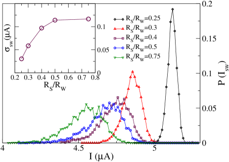
We first calculate the distributions of the switching current in the shunted nanowire for the same temperature . We again simulate Eq.(5) as before by changing the bias current with zero as initial values for and , but now we repeat the full procedure for many realizations of the thermal noise. We count a switch from the metastable to the running state when the nanowire spends more than half the time in the running state over some sufficiently long time period () of simulation. This gives us a distribution for which is plotted in Fig.11 for the shunted wire. We find a good qualitative agreement between the simulation and experiment for the switching distributions of the shunted nanowires as shown in Fig.3 and Fig.11. In the inset of Fig.11 we show the standard deviation of the simulated with and it matches with the trend of the standard deviation of the measured from the experiment. Here we mention that shows a non-monotonic behavior with in the RCSJ model for higher values of , for example, at a constant temperature. This non-monotonic behavior of in the RCSJ model with at a constant temperature is similar to non-monotonic behavior of with temperature for a constant . It will be discussed in the last subsection. However, experimental results show the value of is greater for the unshunted case than the shunted case. This also indicates that the unshunted nanowire is not in a coherent PSC state but is dominated by Joule heating which increases the effective temperature of the wire.
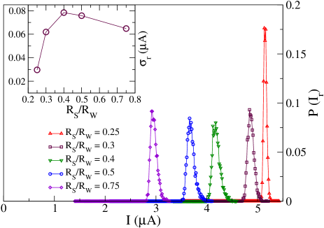
We next simulate the extended RCSJ model to understand the measured distributions of the retrapping current for different shunt resistances. Here we choose a fixed temperature. The simulation method is similar to finding the switching distributions, but now we start from a PSC state with nonzero initial conditions for and . We reduce the bias current and count a retrapping event from the running to metastable state when the nanowire spends less than half of the time in the running state over time period of . The simulated retrapping distributions are plotted in Fig.12 for different values at a constant temperature. We find from Fig.4 that the standard deviation of the retrapping current distributions falls slightly (within the experimental noise limit) with decreasing shunt resistance. The standard deviation of the simulated retrapping current distribution also falls slightly below for which is similar to the experiment. But we also find from the simulation of the RCSJ model that the standard deviation of decays slightly with increasing shunt resistance above for , but it never goes to zero at higher shunt resistances for the RCSJ model with coherent dynamics. The standard deviation of the measured retrapping current distribution for the unshunted wire is almost zero within the noise limit; this is consistent with the existence of JHNS in the unshunted nanowire and PSCs in shunted wires. The width of the simulated switching and retrapping distributions are much greater than the experimental results at the same temperature K. This might be again due to the inductance of the shunt resistor which can effectively reduce the thermal noise in the system.
IV.6 Temperature dependence: shunted vs. unshunted nanowires
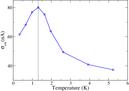
Finally we simulate the extended RCSJ model with an external low shunt resistance to find the temperature dependence of the standard deviation of switching current. We use the same scheme as previous sub-sections to determine the switching current in the simulation at different temperatures. We plot vs. in Fig.13 for and . We find that temperature dependence of simulated due to the thermal fluctuations is non-monotonic just as in the experiment (see Fig.6) for the shunted nanowires. A non-monotonic temperature dependence of due to the thermal fluctuations has also been obtained previously for various JJs Krasnov05 ; Mannik05 ; Krasnov07 and our theoretical analysis not only highlights its ubiquity but also provides a way of obtaining it in terms of a RCSJ kind of modelling. We also find a non-monotonic temperature dependence of the standard deviation of retrapping current in our simulation. In our numerical study here we only consider effect of thermal fluctuations in phase-slips, thus one needs to go beyond the present study to include effect of macroscopic quantum tunneling on the temperature dependence of in the fully quantum regime.
In unshunted nanowires too it has been shown that the standard deviation of the switching current distribution is non-monotonic as a function of temperature Shah08 ; Pekker09 . In the thermal regime at higher temperatures multiple phase slips are required before the wire switches to the normal state and the standard deviation increases as the temperature is decreased Sahu09 . At slightly lower temperatures a single thermal phase slip causes the wire to switch to the normal state and the standard deviation decreases with a decrease in temperature. At low temperatures when QPS are present, depending on how compares with the temperature of crossover from TAPS to the QPS, one can get different behaviors. With an applied external shunt, the increased dissipation is expected to decrease the temperature at which the crossover from thermal activation to MQT takes place.
V Concluding remarks
We have undertaken a detailed study of the effect of external resistance shunts on the behavior of superconducting nanowires. Shunting has a strong effect on the behavior of the nanowire. We find that the statistics of the switching and retrapping currents significantly depends on the value of the shunt resistance. The temperature dependence of the mean switching current in strongly shunted nanowires is consistent with the Bardeen prediction for the temperature dependence of the critical current Bardeen62 ; this indicates that the switching current can be controllably driven very near to the depairing current through external resistive shunting. The retrapping current on the other hand increases and becomes more stochastic, at least for moderate shunting. We demonstrate that the shunting, even with a large resistance value, can be used to control the phase slip events in the wire. We suggest a model based on the Stewart-McCumber RCSJ model, which is generalized to include two resistive elements, corresponding to the effective resistance of the wire (with a phase slip center), and the resistance of the shunt. The model provides a semi-quantitative description to the data. Moreover, it provides insights into developing a circuit-element representation of a superconducting nanowire.
Our work opens up many interesting avenues towards developing a fundamental understanding and control of coherence and dissipation in nanowires as well as its relation to possible quantum phase transitions. It will be important to develop a model that incorporates heating as well as coherent dynamics and studies the entire crossover in going from unshunted nanowires (i.e. infinite shunt resistance in parallel) where heating is most important to the case of very low shunt resistance values where heating is least important. It would be extremely interesting and relevant also to explore the low temperature quantum regime in more detail and to study the implications of our work for quantum computing and other technological applications of nanowires. As an example, nanowires have been used as photon counters Kerman06 , which are important in radioastronomy. The switching events studied in this paper, represent so-called “dark counts”, in the terminology of the photon detection community. Understanding the physics of dark counts is important for the purpose of improving superconducting photon detectors. The fact that the standard deviation of switching current becomes smaller with the inclusion of a shunt resistor has relevance to photon detectors, since dark counts can be reduced by shunting.
VI Acknowledgments
The experimental material is based upon work supported by the U.S. Department of Energy, Division of Materials Sciences under Award No. DE-FG02-07ER46453, through the Frederick Seitz Materials Research Laboratory at the University of Illinois at Urbana-Champaign. Part of the experimental work was carried out in the Frederick Seitz Materials Research Laboratory Central Facilities, University of Illinois. DR and NS acknowledge the University of Cincinnati for financial support while developing the theoretical understanding of the experiment. NS acknowledges the hospitality of Tata Institute of Fundamental Research while working on the manuscript of the paper. Finally, the authors would like to thank Myung-Ho Bae and M. Sahu for fruitful discussions.
Appendix A Resistively and capacitively shunted Josephson junction (RCSJ) model

Here we briefly digress the main features of the RCSJ model (see Fig.14) introduced by Stewart and McCumber Stewart68 ; McCumber68 . We find the equation of motion for the time varying phase difference of the superconducting wave-functions of the circuit in Fig.14 by applying the well-known Josephson dc and ac relations Josephson1 ; Josephson2 ; Josephson3 for the current-phase and the voltage-phase ,
| (9) | ||||
| (10) |
where is the fluctuation-free intrinsic critical current of the junction. The equation of motion for of the circuit in Fig.14 is given by,
| (11) |
along with the Gaussian white noise properties for the Johnson-Nyquist thermal current noise ,
| (12) |
where is the temperature of the JJ with capacitance and resistance . The resistance measures dissipation in the JJ in the finite voltage regime, without affecting the lossless dc zero voltage regime, and indicates the geometric shunting capacitance between the two superconducting electrode Tinkham96 . The Eq.(11) of motion for the junction phase can be rewritten in terms of dimensionless parameters as
| (13) |
where is the quality factor of the linearized equation of motion, , , and is the normalized time. The term is damping as it breaks the time-reversibility of the equation and introduces dissipation. The strength of damping is proportional to and is inversely related to the quality factor. In this notation, the time-averaged steady-state voltage across the junction, . The noise correlation in the scaled time, . The usual McCumber parameter and Stewart parameter with and . For the circuit in Fig.8 we replace in Eq.(11) by where . Then we derive either Eq.(5) or Eq.(8) following the similar steps to get Eq.(13) from Eq.(11).
In the absence of thermal current noise at zero temperature (also neglecting quantum fluctuations), the zero-voltage state or 0 state is stable at all bias levels less than the ideal critical current (), and the voltage state or 1 state is stable at all bias levels greater than a minimum value designated by a fluctuation free re-trapping current . The value of is determined entirely by the quality factor and decreases with increasing as a smaller tilt is sufficient to support the running (finite voltage) state when damping is less. For , the damping is sufficient that a running state is not possible unless the potential decreases monotonically and in this case . For , a running state is possible even when the potential has local minima. Kautz90 In this case and the - curve is hysteretic. In the limit of large , (). Stewart68 ; Kautz90
The phase dynamics described in Eq.(13) can be visualized as the damped motion of a Brownian particle in the tilted washboard potential . In the under-damped regime , the zero-voltage state and the resistive state correspond to the particle trapped by the energy barrier and running downward along the tilted potential, respectively. Escape from the potential (0 state to 1 state) can occur even for due to the thermal and the quantum fluctuations.
References
- (1)
- (2)
- (3)
- (4)
- (5) W. A. Little, Phys. Rev. 156, 396 (1967).
- (6) A. Bezryadin, J. of Phys. Condens. Matter 20, 043202 (2008).
- (7) N. Giordano, Phys. Rev. B 41, 6350 (1990).
- (8) A. Bezryadin, C. N. Lau, M. Tinkham, Nature 404, 971 (2000).
- (9) D. S. Golubev and A. D. Zaikin, Phys. Rev. B 64, 014504 (2001).
- (10) C. N. Lau, N. Markovic, M. Bockrath, A. Bezryadin, and M. Tinkham, Phys. Rev. Lett. 87, 217003 (2001).
- (11) M. Tian, et. al., Phys. Rev. B 71, 104521 (2005).
- (12) F. Altomare, A.M. Chang, M. R. Melloch, Y. Hong and Charles W. Tu, Phys. Rev. Lett. 97, 017001 (2006).
- (13) M. Zgirski, K.-P.Riikonen, V. Touboltsev and K. Yu. Arutyunov, Phys. Rev. B 77, 054508 (2008).
- (14) M. Sahu, Myung-Ho Bae, A. Rogachev, D. Pekker, Tzu-Chieh Wei, N. Shah, Paul. M. Goldbart, and A. Bezryadin, Nat. Phys. 5, 503 (2009).
- (15) Peng Li, Phillip M. Wu, Yuriy Bomze, Ivan V. Borzenets, Gleb Finkelstein, and A. M. Chang, Phys. Rev. Lett. 107, 137004 (2011).
- (16) A.V. Lopatin, N. Shah and V. M. Vinokur, Phys. Rev. Lett. 94, 037003 (2005).
- (17) N. Shah and A.V. Lopatin, Phys. Rev. B 76, 094511 (2007).
- (18) G. Refael, E. Demler, Y. Oreg and D. S. Fisher, Phys. Rev. B (Condens. Matter Materials Phys.) 75, 014522 (2007).
- (19) A. Del Maestro, B. Rosenow, N. Shah and S. Sachdev, Phys. Rev. B 77, 180501 (2008).
- (20) A. Del Maestro, B. Rosenow, M. Müller and S. Sachdev, Phys. Rev. Lett. 101, 035701 (2008).
- (21) A. T. Bollinger, R. C. Dinsmore, A. Rogachev and A. Bezryadin, Phys. Rev. Lett. 101, 227003 (2008).
- (22) A. Schmid, Phys. Rev. Lett. 51, 1506 (1983).
- (23) S. A. Bulgadaev, JETP Lett. 39, 315 (1984).
- (24) S. Chakravarty, Phys. Rev. Lett. 49, 681 (1982).
- (25) A. D. Zaikin, D. S. Golubev, A. van Otterlo, G. T. Zim¡nyi, Phys. Rev. Lett. 78, 1552 (1997).
- (26) J.S. Penttilä, Ü. Parts, P. J. Hakonen, M. A. Paalanen, E. B. Sonin, Phys. Rev. Lett. 82, 1004 (1999).
- (27) H. P. Büchler, V. B. Geshkenbein, G. Blatter, Phys. Rev. Lett. 92, 067007 (2004).
- (28) P. Werner and M. Troyer, Phys. Rev. Lett. 95, 060201 (2005).
- (29) D. Meidan, Y. Oreg and G. Refael, Phys Rev. Lett. 98, 187001 (2007).
- (30) M. Tinkham and J. U. Free, C. N. Lau, and N. Markovic, Phys. Rev. B 68, 134515 (2003).
- (31) N. Shah, D. Pekker and P. M. Goldbart, Phys. Rev. Lett. 101, 207001 (2008).
- (32) D. Pekker, N. Shah, M. Sahu, A. Bezryadin, and Paul. M. Goldbart, Phys. Rev. B 80, 214525 (2009).
- (33) J. E. Mooij and C. J. P. M. Harmans, New J. of Phys. 7, 219 (2005).
- (34) J. E. Mooij and Y. V. Nazarov, Nature Physics 2, 169 (2006).
- (35) M. Tinkham, Introduction to Superconductivity (McGraw-Hill, New York, 1996), 2nd ed.
- (36) E. Ben-Jacob, D. J. Bergman, B. J. Matkowsky, and Z. Schuss, Phys. Rev. A 26, 2805 (1982).
- (37) J. M. Martinis and R. L. Kautz, Phys. Rev. Lett. 63, 1507 (1989).
- (38) D. Vion, M. Götz, P. Joyez, D. Esteve, and M. H. Devoret, Phys. Rev. Lett. 77, 3435 (1996).
- (39) J. M. Kivioja, T. E. Nieminen, J. Claudon, O. Buisson, F. W. J. Hekking, and J. P. Pekola, Phys. Rev. Lett. 94, 247002 (2005).
- (40) V. M. Krasnov et. al., Phys. Rev. Lett. 95, 157002 (2005).
- (41) J. Männik, S. Li, W. Qiu, W. Chen, V. Patel, S. Han, and J. E. Lukens, Phys. Rev. B 71, 220509(R) (2005).
- (42) V. M. Krasnov, T. Golod, T. Bauch, and P. Delsing, Phys. Rev. B 76, 224517 (2007).
- (43) Myung-Ho Bae, M. Sahu, Hu-Jong Lee, and A. Bezryadin, Phys. Rev. B 79, 104509 (2009).
- (44) S. Takaqi, Macroscopic Quantum Tunneling (Cambridge University Press July 2005).
- (45) A. J. Leggett, J. Phys. (Paris), Colloq. 39, C6-1264 (1978).
- (46) A. O. Caldeira and A. J. Leggett, Phys. Rev. Lett. 46, 211 (1981).
- (47) A. J. Leggett, Lesson of Quantum Theory, N. Bohr Centenary Symposium, 35-57 (1986).
- (48) A. J. Leggett, S. Chakravarty, A. T. Dorsey, M. P. A. Fisher, A. Garg, and W. Zwerger, Rev. Mod. Phys. 59, 1 (1987).
- (49) R. F. Voss and R. A. Webb, Phys.Rev.Lett. 47, 265 (1981).
- (50) J. M. Martinis, M. H. Devoret, and J. Clarke, Phys. Rev. B 35, 4682 (1987).
- (51) J. M. Martinis and H. Grabert, Phys. Rev. B 38, 2371 (1988).
- (52) W. C.Stewart, Appl. Phys. Lett. 12, 277 (1968).
- (53) D. E. McCumber, J. Appl. Phys. 39, 3113 (1968).
- (54) K.K. Likharev, Dynamics of Josephson junctions and circuits (Gordon and Breach Science Publishers, New York, 1981).
- (55) S. Al-Khawaja, Chaos, Solitons and Fractals, 36, 382 (2008).
- (56) S. Naito and Y. Higashino, Jpn. J. Appl. Phys. 23, 861 (1984).
- (57) B. Dimov, et al., IEEE Transactions on Applied Superconductivity, 15, 2 (2005).
- (58) A. Bezryadin and C. Dekker, J. Vac. Sci. Technol. B 15, 793 (1997).
- (59) J. S. Langer and A. Ambegaokar, Phys. Rev. 164, 498 (1967).
- (60) D. E. McCumber and B. I. Halperin, Phys. Rev. B 1, 1054 (1970).
- (61) M. Tinkham and C. N. Lau, Appl. Phys. Lett. 80, 2946 (2002).
- (62) J. Bardeen, Rev. Mod. Phys. 34, 667 (1962).
- (63) Y. C. Chen, M. P. A. Fisher, and A. J. Leggett, J. Appl. Phys. 64, 3119 (1988).
- (64) R. C. Dinsmore III, Myung-Ho Bae, A. Bezryadin, Appl. Phys. Lett. 93, 192505 (2008).
- (65) W. J. Skocpol, M. R. Beasley, and M. Tinkham, J. Low Temp. Phys. 16, 145 (1974).
- (66) V. Ambegaokar and B. I. Halperin, Phys. Rev. Lett. 22, 1364 (1969); 23, 274 (1969).
- (67) J. Kurkijarvi and V. Ambegaokar, Phys. Lett. 31A, 314 (1970).
- (68) M. P. Allen and D. J. Tildesley, Computer Simulation of Liquids, Clarendon Press.
- (69) A. B. Cawthorne, C. B. Whan, and C. J. Lobb, J. Appl. Phys. 84, 1126 (1998).
- (70) A.J. Kerman, E. A. Dauler, W. E. Keicher, J. K. W. Yang, K. K. Berggren, G. Gol’tsman, B. Voronov, Appl. Phys. Lett. 88, 111116 (2006).
- (71) L. P. Gor’kov, Exptl. Theoret. Phys. (U.S.S.R.)34, 735 (1958); English transl.:Soviet Phys. JETP 7 505 (1958).
- (72) B. D. Josephson, Phys. Lett. 1, 251 (1962).
- (73) P. W. Anderson and A. H. Dayem, Phys. Rev. Lett. 13, 195 (1964).
- (74) R. L. Kautz and J. M. Martinis, Phys. Rev. B 42, 9903 (1990).