Possible superconductivity in multi-layer-graphene by application of a gate voltage
Abstract
The carrier density in tens of nanometers thick graphite samples (multi-layer-graphene, MLG) has been modified by applying a gate voltage () perpendicular to the graphene planes. Surface potential microscopy shows inhomogeneities in the carrier density () in the sample near surface region and under different values of at room temperature. Transport measurements on different MLG samples reveal that under a large enough applied electric field these regions undergo a superconducting-like transition at K. A magnetic field applied parallel or normal to the graphene layers suppresses the transition without changing appreciably the transition temperature.
keywords:
Multi-layer-graphene , electrical properties , superconductivity1 Introduction
Superconductivity in carbon based materials has been found in a relatively large number of samples. Most of them are graphite based systems with a chemical doping. Intercalated graphite compounds with doping elements as potassium (C8K)[1], Lithium (C2Li)[2], Calcium (C6Ca)[3] or Ytterbium (C6Yb)[3] are found to be superconducting with transition temperatures () from 1.9 K (for C2Li)[2] up to 11.5 K (for C6Ca)[3]. Note that in all those cases the superconducting state is obtained in materials with much less anisotropy as pure graphite with its Bernal structure. Recently published works indicate, however, the possibility of higher in graphite systems, namely: The magnetic response of water-treated graphite powders suggests the existence of room temperature superconductivity [4], supporting the conclusion of old reports [5, 6]; Measurements testing directly the embedded two dimensional interfaces found within the graphite Bernal structure show evidence for the Josephson effect at temperatures clearly above 100 K[7]; Magnetization measurements performed on graphite samples with internal interfaces support the existence of a superconducting-like behaviour [8] at very high temperatures.
Previous work reported that sulfur-doped graphite composites shows superconducting-like behavior up to 35 K [9]. Recently published study [10] reported that bringing alkanes into contact with graphite surfaces triggers zero resistance at room temperature. By doping graphite samples via phosphorous or argon implantation, several superconducting-like steps in the resistance vs. temperature were reported recently up to nearly room temperature111Larkins, G., Vlasov, Y. Holland, K.. ArXiv:1307.0581. We may therefore speculate that if the carrier density increases in the graphene layers superconductivity might be triggered. Although we should note that, taking into account the clear difference between the critical temperatures obtained in intercalated graphite compounds and those in doped but not intercalated graphite, it appears that the critical temperature increases the higher the anisotropy of doped graphite.
Most of the theoretical predictions about superconductivity in graphite/graphene emphasize that it should be possible under the premise of sufficiently high carrier density to reach K [11, 12, 13]. Following a BCS approach in two dimensions energy gap values at 0 K of the order of K have been obtained if the density of conduction electrons per graphene plane increases to cm-2 [11], in agreement with the theoretical estimates based on different approaches[12, 13]. Also high temperature superconductivity with a pairing symmetry has been predicted to occur in doped graphene with a carrier concentration cm-2[14]. We note that the intrinsic carrier density of defect-free graphene layers inside graphite is cm-2[15, 16, 17]. However, defects and/or hydrogen doping within regions at interfaces[18] or at the graphite surface may show much larger carrier density, e.g. cm-2. Therefore it is a challenge for experimentalists to increase the carrier density above a certain threshold, at the interfaces or at the regions that provide a coupling to those interfaces, to trigger superconductivity. The interfaces we are taking about are quasi two-dimensional regions that are located between two crystalline regions with Bernal stacking order each of them with a slightly different angle respect to the axis [18, 7].
We note that high temperature superconductivity has been also predicted to occur at rhombohedral graphite surface regions due to a topologically protected flat band [19, 20] or in multilayered structures with hybrid stacking, i.e. rhombohedral and Bernal stacking [21]. In this case, however, increasing the carrier density will not necessarily increase . A homogeneous doping strongly suppresses surface superconductivity while non-homogeneous field-induced doping has a much weaker effect on the superconducting order parameter [21]. Therefore, the expected effect of an electric field on the transport properties of inhomogeneous doped multilayered graphite appears not so simple.
Recently published studies show that electrostatic carrier accumulation is an interesting tool to trigger new states of matter at certain interfaces. In the particular case of graphite Otani and collaborators predicted that nearly free electron states distributed in quasi two dimensional () regions at the interfaces can cross the Fermi level if an external electric field perpendicular to the graphene plane is applied [22]. This opens the possibility of triggering superconductivity in a pure carbon material. It is then appealing to use the electrostatic charge doping to increase in graphite without disturbing its quasi- dimensionality. This expected difference in critical temperatures can be partially understood within a BCS mean field model taking into account the role of high-energy phonons in the graphite structure itself[11]. Metal decorated graphene samples have been proven to have a tunable superconducting to insulating transition via electric field gating [23],[24] where both chemical and electrostatic carrier density doping are combined. However, no experimental results for pure graphite samples have been published yet. Thus, the aim of the present study is to induce large enough charge densities inside the MLG samples via electric field gating without any chemical doping.
2 Experimental details
2.1 Samples characteristics
The MLG samples were prepared from Highly Oriented Pyrolytic Graphite (HOPG) flakes with the highest crystalline quality, ZYA grade (0.4∘ rocking curve width) from the former company Advanced Ceramics. Small flakes from the as-received bulk piece of HOPG were produced by peeling. These small flakes were used to produce the so-called multi-layer-graphene samples by a simple rubbing procedure described elsewhere [18] . This procedure consists in a careful mechanical press and rubbing of the initial material on a previously cleaned substrate. All the samples were fixed on a 150 nm thick Si3N4 terminated surface of a doped Si substrate. Samples with thicknesses between 20 to 90 nm (measured by Atomic Force Microscopy (AFM) and optical microscopy) have been obtained. The electrical contacts were prepared using electron beam lithography followed by Pt/Au thermal evaporation, see Fig.1(a). The distance between voltage electrodes varied between and 4m, upon sample. Samples quality has been checked by measuring Raman spectra (see Supporting information).
Regarding the possible influence of the used preparation procedure on the existence and distribution of the superconducting regions in the studied samples, we note the following. In [18] it has been shown that the temperature dependence of the resistance of samples obtained from the same HOPG bulk sample as used in this work, is related to the existence of internal interfaces. Neither Raman nor the transport measurements of several samples prepared with the rubbing method indicate any relevant influence. The interfaces, which existence has been known for a relatively long time [25], are found in some, not all, HOPG samples. The superconducting properties due to these interfaces remain, independently of the method used to prepare the samples obtained from the same bulk HOPG [7, 26]. Therefore, there is no clear experimental evidence that speaks for or against an influence of the rubbing method on the transport characteristics of the samples.
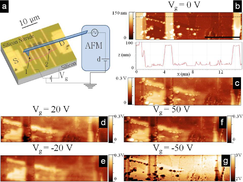
The samples surfaces have been studied by Atomic Force Microscopy (AFM). We used a Dimension 3000 scanning probe microscope with a Nanoscope IIIa controller and phase extender (Digital Instruments Inc., Santa Barbara, CA). A sketch of the experimental setup is shown in Figure 1(a) where the AFM and the gate voltage supply are presented. Note that both devices have common ground and that the configuration used allows us to create an external electric field perpendicular to the graphene planes. The gate voltage was applied between the conducting doped Silicon substrate and the sample surface through the large electrical resistance of the 150 nm Si3N4 layer. Every experiment has been operated within the non-breaking range of this insulating layer.
An optical microscope image of sample S5 is shown in figure 1(a); numbers and refer to different studied areas. In figure 1(b) an AFM image of the topography of a part of this sample (m m) is presented. The brightest areas correspond to the electrical contacts and the two darker stripes in the middle of the image correspond to two destroyed electrical contacts. Besides that, the sample appears to be flat. As we are interested in studying the carrier density distribution in the near surface region we have performed surface potential measurements, also known as Kelvin probe microscopy (KPM)[27]. In this operating mode we record the voltage on the sample surface in the following way. In a first scan the sample topography is recorded. In a second scan at a height of 50 nm above the sample surface the Coulomb interaction between tip and sample is eliminated by applying a voltage equal to the difference of the work-functions of sample and tip controlled by a feedback loop. In principle, we may expect that voltage variations on the sample indicate different Fermi levels and thus different carrier densities as the whole sample is a piece of multigraphene, apart from the gold contacts.
Figure 1(c) shows the phase image obtained without any applied gate voltage ( = V). One can easily realize that the obtained signal from the sample surface is not homogeneous, i.e. it shows a location dependent work-function. It can clearly be seen also that different potentials are closely related to different surface features. The most probable scenario is the one related to the surface filth or adsorption of molecules proposed and measured in [28] . Figures 1(d) to (g) show the effect of different on the sample surface potential. For V (Figures 1(d) and (e)), no remarkable change with respect to no applied electric field is observed. No essential effect is observed at higher positive (see Figure 1(f) obtained at V). However, if we use V, see Figure 1(g), we recognize a clear change where brighter areas are detected with a larger potential variation within the measured region. Taking into account the scales on the right of each image, we can see that in the case of Figure 1(g) the variation is V, while in the rest of the cases is 0.3 V.
The important message for this work is that different sample regions apparently react differently, i.e. the electrical field induces heterogeneous doping pointing to intrinsic variations of the electronic structure. This provides us a way to understand the non percolative superconducting transition we describe below. It can be understood taking into account that an ideal graphite matrix with Bernal stacking is semiconducting[29] and that internal interfaces[18, 7, 8] plus other defects[15] affect the effective carrier density and therefore the screening characteristics in specific regions. Summarizing, we observed an inhomogeneous surface potential response, which reacts asymmetrically to the electric fields applied perpendicular to the graphene planes.
In order to further investigate the effect of the gate voltage on the carrier density of MLG samples we studied the transport properties, i.e. resistance behavior as function of temperature and magnetic field. We use a DC input current of A supplied by a Keithley 6221 current source and the voltage was measured with a Keithley 2182 DC nanovoltmeter, always using the usual four probe method. When we apply a gate voltage the configuration shown in Figure 1(a) is the one used for all the samples.
The measurements as a function of temperature and magnetic field were performed in a He-flow cryostat (Oxford Instruments) in the temperature range between 2 K and 250 K with temperature stabilization better than 1 mK. The magnetic field was applied with a superconducting solenoid in permanent modus. Its value was obtained from a previously calibrated Hall sensor located on the sample holder. The magnetic field was applied perpendicular as well as parallel to the main area of the samples (i.e. graphene planes) using a step-motor controlled sampler holder rotation system. The measurements were done as follows: first, we applied the corresponding at 2 K and after a stable value of the resistance was reached a certain magnetic field was applied. Then, the resistance was measured from 2 K to 25 K. Once the curve was measured, the magnetic field was set to zero and the process was repeated from 2 K with other set field. The gate voltage has been maintained during the whole set of measurements.
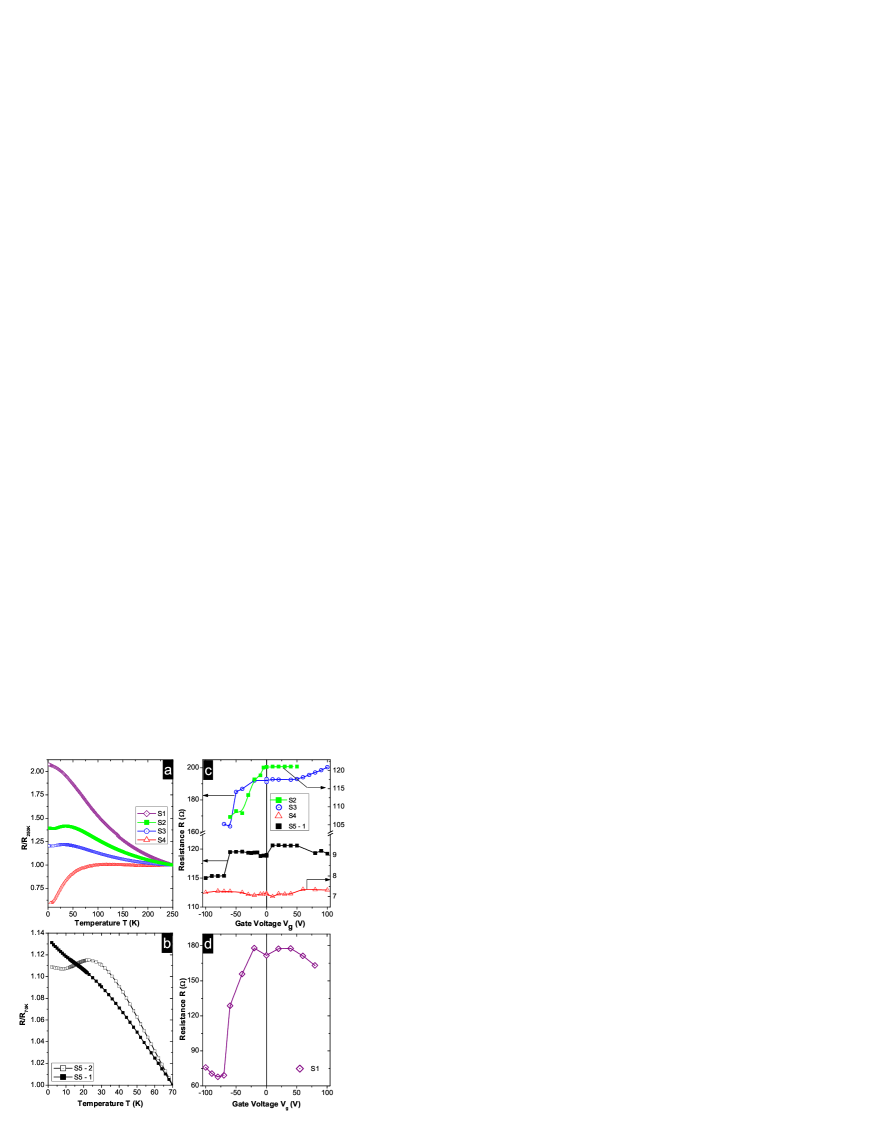
The temperature dependence of the resistance at zero gate voltage is shown in Figures 2(a) and (b). We present here the results of five samples named S1, S2, S3, S4 and S5, showing slightly different behaviors. S1, S2 and S3 samples (30-45, 22, 30-45 nm thickness) show a semiconducting behavior intrinsic to the graphite Bernal structure influenced partially by lattice defects, especially interfaces[29]. Sample S4 (90 nm thickness) shows a clear metallic behavior below 100 K ascribed to its higher number of internal interfaces [18]. The level off of of sample S1 below 25 K and the features below 50 K in samples S2 and S3, are also related to the role of these interfaces and/or to the contributions of the free surface of the sample (or sample-substrate interface), as discussed in Refs. [18] and [29]. The results for sample S5 (non-homogeneous thickness 20-35 nm) obtained at the two different regions labeled 1 and 2 in Figure 1(a) are shown in Figure 2(b). While in the region the semiconducting behavior remains even at low temperatures, the behavior of the sample area reveals a similar level off or maximum as in samples S1, S2 and S3, which is related to the contribution of the internal interfaces and other lattices defects in the sample regions where the voltage electrodes are located. The clear difference in the function within a few microns distance within the same sample is in qualitative agreement with the surface potential microscopy results shown previously as well as similar transport results obtained in thin graphite samples[15] and earlier EFM results on bulk HOPG sample surfaces[30] that revealed sub-micrometer domain like carrier density distributions in graphite surfaces.
2.2 Electrostatic screening in MLG samples
Different theoretical approaches calculated the distribution of charge under an external electrical field perpendicular to the graphene planes in graphite[31],[32]. Using a random phase approximation, depending on whether the inter-layer electron tunneling was taken into account or not, screening lengths between nm[31] and nm[32] have been obtained. However, Miyazaki and collaborators experimentally measured a screening length of nm [33], which corresponds to 3 or 4 graphene layers. Kuroda and coworkers theoretically found that the actual screening depth depends on the experimental conditions, in particular the actual doping of the sample and the temperature[34]. Furthermore, they found that a variation of more than an order of magnitude can be obtained. We use their model to estimate the penetration depth of the applied electric field inside our samples.
The intrinsic carrier density in each graphene layer in the graphite structure, without defects and interfaces, should be cm-2 at the temperature of our experiments [15],[16],[35]. The exact value of for the graphene layers in each of the measured samples is not really well known just because the samples are not free from defects and impurities as, e.g., hydrogen. We take as upper limit cm-2 for the graphene layers not involved in the internal interfaces or at the surface. Following [34] we estimate that at K the effective penetration depth should be equal to at least 7 graphene layers or about 2.4 nm. That would mean that the electric field mainly influences the near surface region of the samples, in case that no internal interfaces with much larger carrier density exist. Otherwise, if the carrier density is larger, the screening effect will be more relevant. Our estimate is basically in agreement with other theoretical work, which showed that the electric field should be screened within a few layers from the sample surfaces [36]. In case the carrier density of the non-defective graphene layers is smaller, the larger will be the penetration depth of the electric field in the sample.
3 Results
3.1 Gate voltage effect
Although few layer graphene systems have been extensively studied, the properties of graphene-based systems with a higher number of layers ( or more) are still a matter of discussion. Particularly, the gate voltage effect is not fully clarified probably because the complexity related to the screening effect, the dependence on the number of layers and the corresponding presence (or absence) of interfaces with higher carrier densities[18],[29],[7] as well as further inhomogeneities due to lattice defects and impurities. These facts make essentially every sample slightly different from the others and even different regions within the same sample can show noticeable differences concerning the electronic properties, as the results for sample S5 in Figure 2(b) demonstrate (see also [15] particularly the results in Figure 4).
Due to the electrostatic screening in MLG samples, it is essential to apply a large amplitude of the electric field on the sample in order to see an effect on the electrical resistance. Typical gate voltage values for MLG samples on SiO2 of 300 nm thickness substrates are 100 V[37]. Otani and coworkers calculated an electric field of 0.49 V/ in order to inject free-electron carriers at the Fermi level[22]. As the number of layers in our samples is larger than in their work, we use back gate voltages up to 100 V.
Figures 2(c) and (d) show the resistance vs. applied gate voltage at a constant temperature of 2 K for samples S1 to S5, this last in region . With exception of the thickest sample S4, all samples show an asymmetric behavior respect to zero voltage with a clear decrease of the resistance at certain negative ’s. For positive voltages the resistance either increases slightly or it does not change significantly. We think that these differences, as well as that in the relative decrease of resistance at a given negative gate voltage, are related to the overall inhomogeneities of the MLG samples due to impurities or to the higher carrier densities located at the internal interfaces of the samples. The absence of any significant change with in the thickest sample S4 is a clear indication for the screening effect of the electric field. A similar behavior of the resistance of MLG samples with the applied gate voltage was partially reported by Kim and collaborators[38]. However, in that work no results on the temperature or the magnetic field dependence of the resistance under a gate voltage were reported.
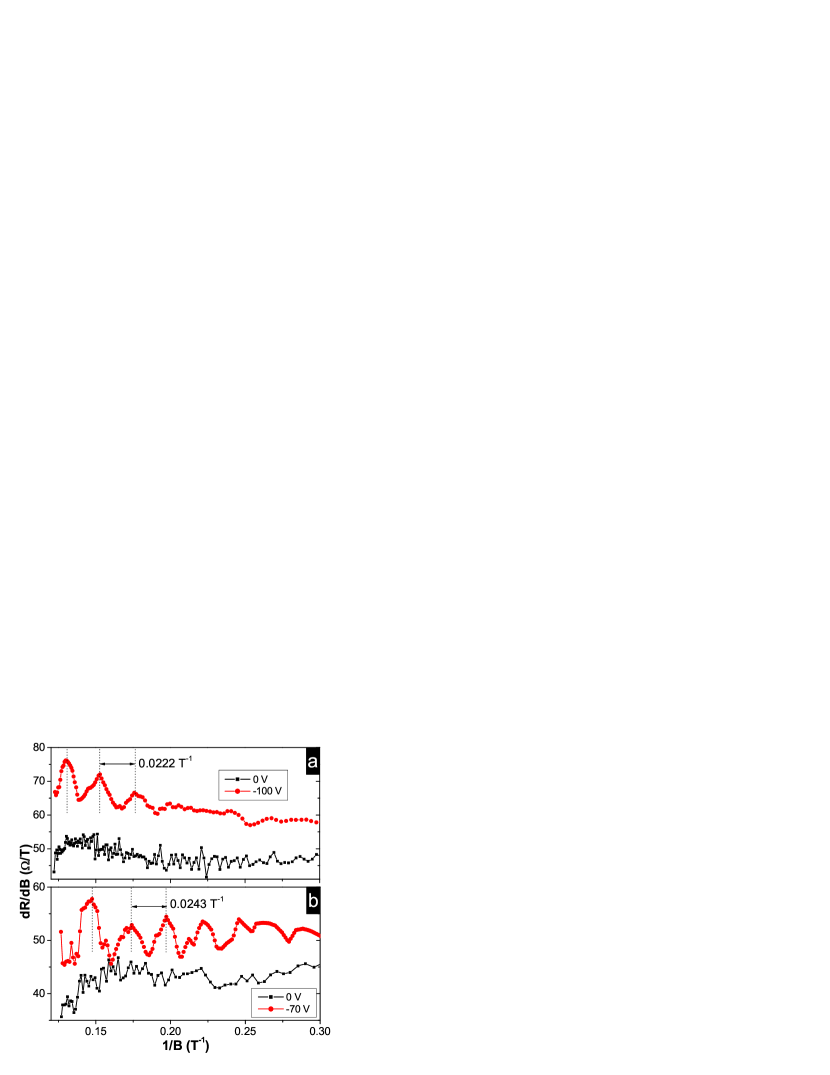
The clear drop observed in the resistance for large enough negative in different MLG samples suggests the existence of a superconducting-like transition that should be also recognized as a function of temperature, as shown below. The overall change of the resistance with indicates that there might be an increase of the carrier density at the Fermi level in some parts of the sample. A way to check whether there is a real increase in the carrier density with applied gate voltage is to measure the Shubnikov-de Haas (SdH) oscillations of the magnetoresistance. Figure 3 shows the first field derivative of the magnetoresistance vs. inverse field at 2 K with and without applied gate voltage corresponding to sample S1 (a) and sample S5 region (b), as examples. At no applied gate voltage the data reveal no SdH oscillations in the shown field range and within experimental error. This is actually expected because ideal graphite is a narrow band semiconductor and at low temperatures no Fermi surface should exist[29]. At a large enough applied gate voltage clear SdH oscillations are observed in the first field derivative for fields above T. From the obtained period of the oscillations we estimate a carrier density cm-2 for S1 and cm-2 for S5 at region , one order of magnitude larger that the one obtained for the bulk graphite sample[15] from which the MLG samples were obtained.
We stress that the carrier density obtained for the bulk sample is not intrinsic of the Bernal graphite structure but it is related mainly to the internal interfaces (or other defective regions[15],[29]) commonly found in the used highly oriented pyrolytic graphite samples[18]. We note also that the rather weak SdH oscillations are observed only at fields above 1 T indicating the existence of domains of size nm in which nm, i.e. domains with cm-2 within a matrix of much lower carrier concentration (i.e. cm-2[17]) ( and are the cyclotron radius and Fermi wavelength, respectively)[15]. Therefore, we can assume that, if the distance between the high carrier density domains is about the same as the domains size, the applied gate voltage couples these high carrier density localized domains. In this case the decrease of the resistance observed in Figures 2(c) and (d) for large enough negative can be understood.
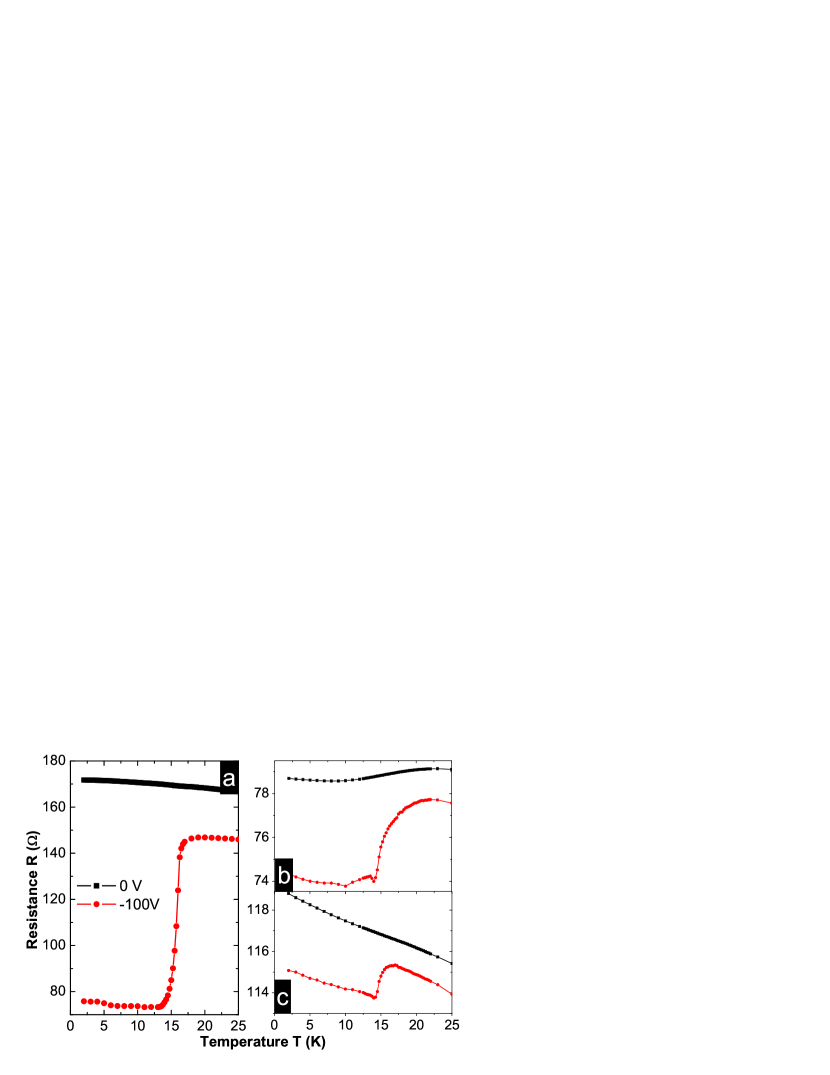
In order to further investigate the effect of the gate voltage on the electronic properties, the temperature dependence of the resistance under a constant gate voltage has been studied. Figure 4 shows the results obtained for samples S1 and S5 without applied gate voltage and with V. A clear step like transition below 20 K appears if is applied. The details of the transition depend on the selected sample (see Supporting information). Even the two studied regions in sample S5 present some differences (see Figure 4 (b) and (c)), again a sign of the existence of inhomogeneities in the samples. The observed transition at K indicates that after the application of a negative large voltage the large carrier density located in some parts of the samples (as shown in the SdH oscillations in Figure 3) induces either superconductivity in those parts or they provide a kind of Josephson link between superconducting regions already existent in the samples at certain interfaces[7]. Which of these two possibilities is the correct description can be answered measuring the magnetic field dependence of the resistance, as we show below. For both cases it applies that the reason for non percolation, i.e. non zero resistance in the presumable superconducting state, is simply related to the fact that the voltage electrodes are not contacting the superconducting regions directly.
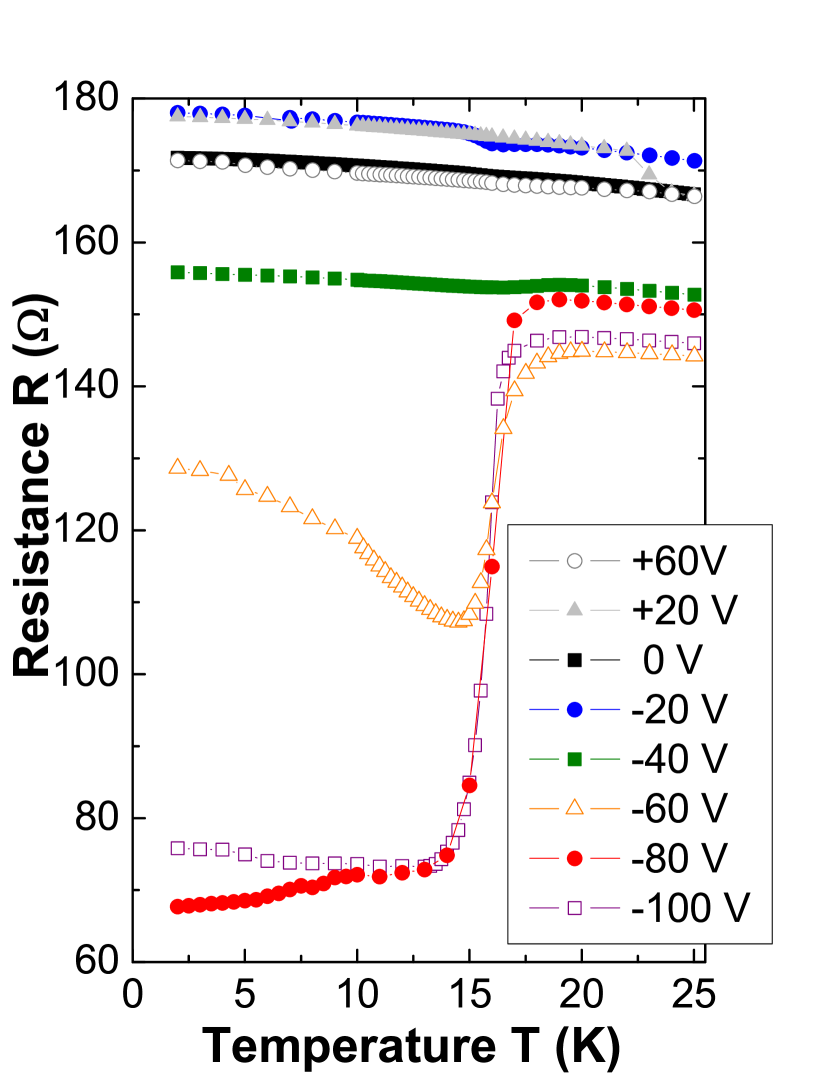
The effect of different gate voltages on the temperature dependence of the resistance was also investigated (see Figure 5) and the asymmetric behavior of the resistance with (see Figure 2) is recognized. The temperature dependence of the resistance does not change significantly for V. The change in resistance produced at -20 V V remains small (less than 5%) and it is not monotonous, see Fig. 5. At V a small dip appears at K. For V the small dip develops in a clear step with less than 2 K transition width. The curve obtained at V shows a drop of the resistance at 15 K and an upturn below it. This indicates the existence of a non-uniform channel with superconducting regions connected in series with normal ones. As shown in Figure 5 for sample S1, the lower the gate voltage the clearer the transition. Note that the transition temperature does not change with the applied gate. This general behavior observed in all samples suggests that the increase in carrier density is not really triggering a superconducting transition but it enables a link between the already existent superconducting regions. This result would indicate that field-induced superconductivity should not be observed in single graphene or MLG samples without interfaces (or the regions where superconductivity is localized).
3.2 Magnetic field effect under a finite gate voltage
For a better characterization of the nature of the observed transition under an applied electric field we need to study the magnetic field effect on it. We have measured therefore the temperature dependence of the resistance under a large enough gate voltage at constant magnetic fields. In what follows we discuss mainly the results of sample S1 for both, magnetic field applied normal and parallel to the graphene planes. Results for the other samples are qualitatively similar. Figure 6 shows the dependence of the resistance with temperature at different applied fields normal to the main area of the sample and at a fixed gate voltage of -100 V. As expected for this field direction, the background resistance increases with field due to the usual magnetoresistance of the MLG samples, see Figure 6(a). To suppress the effect of the magnetoresistance contribution and show clearer the effect of the magnetic field on the transition, Figure 6(b) shows the same data as in (a) but normalized.. As shown in Figure 6 a field of 0.2 T is enough to suppress completely the transition at 17 K. This suppression remains to a field of 1.5 T. At a field of 3 T and higher the transition appears again at the same temperature but slightly broader and it nearly vanishes at 8 T, see Figure 6(b). Note that the temperature of the transition does not change significantly with applied field. The transition is rather unconventional because the magnetic field affects mainly the relative step height of the transition. This fact also suggests that the field does not affect the superconducting regions themselves but mainly the coupling between them produced by the applied electric field, indicating also that the upper critical field would be higher than 8 T. A similar conclusion can be taken from the increasing difference between FC and ZFC magnetic moment data at high-fields, see Fig. 6 in the supporting information of Ref. [4].
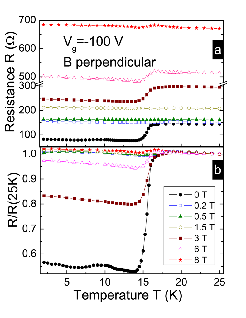
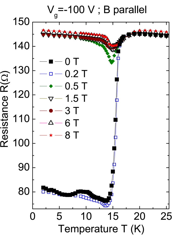
Figure 7 shows the resistance vs. temperature at V and at different magnetic fields applied parallel to the graphene planes of the sample. The misalignment of the field is less than . The measured data show that the transition remains unaffected by a parallel field of 0.2 T, in contrast to the normal field result. At higher fields, however, it is suppressed monotonously without any sign for a reentrance. Note that the resistance above K does not change practically with field in agreement with the fact that the magnetoresistance of graphite depends mainly on the normal field component to the graphene planes[39]. This indicates clearly the absence of any Lorenz-force driven effect or a change in the electron system at all above the critical temperature. As for the normal applied fields, for parallel applied fields the transition does not shift significantly to lower temperatures and the resistance shows a minimum just below the transition.
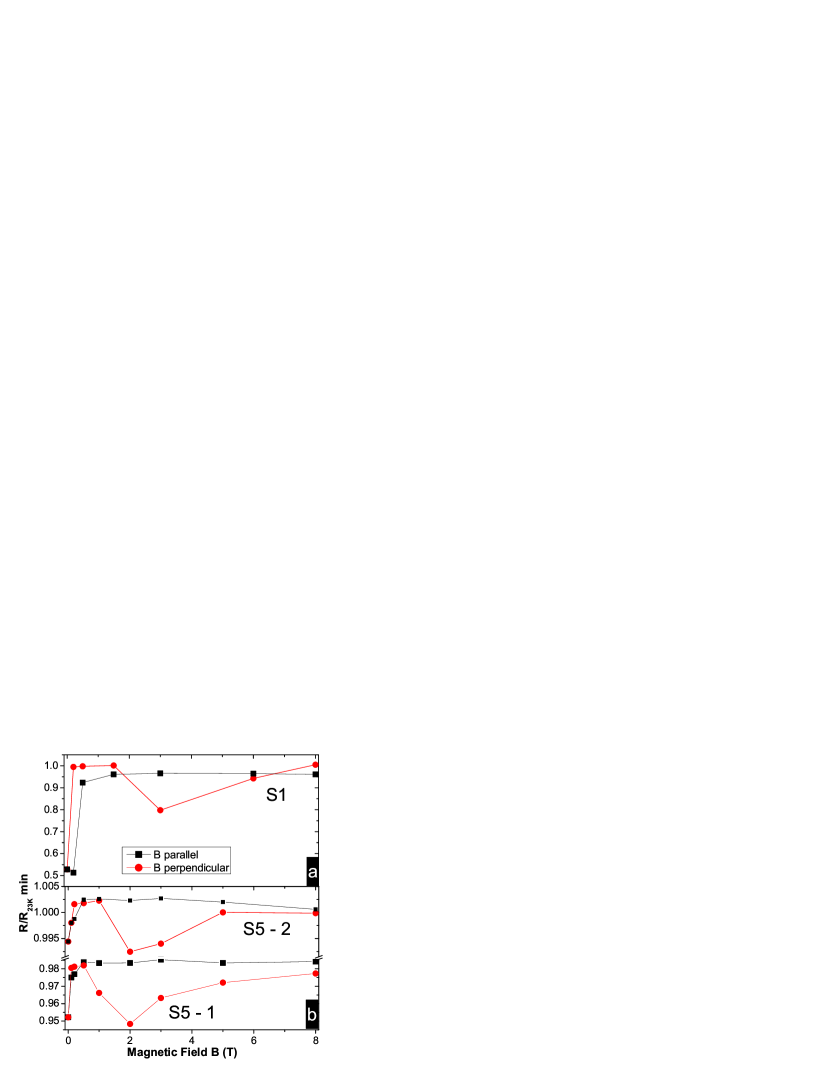
The magnetic field behavior of the transition for both field directions, i.e. the resistance below the transition increases with field without a clear decrease of the transition temperature within the used field range, suggests that a filamentary superconducting path produced by the applied gate voltage is affected by the magnetic field. In Figure 8 we compare the results for both field directions by plotting the minimum resistance just below the transition normalized by the resistance value at 23 K vs. applied field for samples S1 and S5 in both studied regions. Although some differences appear between S1 and S5, we obtain qualitatively the same results, i.e., a small perpendicular field of 0.1T is enough to vanish the transition and a reentrance is observed at high enough applied magnetic field normal to the graphene layers. The rather weak anisotropy of the low field necessary to affect the transition peaks for the triggering of a filamentary path by the electric field.
The main difference in the behaviors obtained as a function of field direction is related to the reentrance observed only for fields normal to the graphene planes. The reentrance of the transition observed for this configuration appears to have an orbital character. We note that a similar effect has been observed through the measurement of the conductance of a high-mobility 2D electron gas between superconducting contacts at high fields applied normal to the main 2D area[40]. This reentrance or increase in the conductance with magnetic field was explained arguing the increase in the probability of Andreev reflections above a certain field[40]. A comparison of our results with those from [40] is permissible because the carriers mobility in the graphene layers of our samples is huge[16] and indications for the influence of Andreev reflections in the magnetoresistance have been also reported in similar MLG[41].
4 Conclusion
We studied the behavior of the resistance of several MLG samples as a function of temperature and magnetic field and under the influence of a gate voltage applied normal to the graphene planes. Taking into account relevant literature on granular superconductors as well as the one obtained recently for the internal interfaces in graphite samples, it appears natural to assume that the transition in the resistance that develops at K with negative gate voltage is related to a non-percolative superconducting-like state. Several open questions remain, as for example why the apparent transition temperature is about 17 K and not at much higher temperatures, as measured from direct measurements of the response of the embedded interfaces in graphite lamellae[7],[8] or in water treated graphite powders [4]. A possible answer to this important question is probably related to the electric field triggering of the (and not ) connecting paths between the already superconducting regions, these last much less influenced by the electric field. In this case the superconductivity temperature in graphite should be much near the graphite intercalated compounds[1],[3] than in the discovered superconductivity. The observed magnetic field effects would influence the connecting paths and not the intrinsic superconducting regions. Three dimensional paths and not only appear necessary in order to explain the weak field anisotropy. Finally, we would like to note the report on gate-induced superconductivity in carbon nanotubes[42] at temperatures above 12 K, results that support the findings of these studies.
Acknowledgement
This work was supported by the Deutsche Forschungsgemeinschaft under contract DFG ES 86/16-1 and by the DAAD project Nr.56269524 under PROBRAL and CAPES. R.R.d.S. and Y.K. acknowledge the support from FAPESP, CNPq, CAPES-PNPD 1571/2008, ROBOCON, and INCT NAMITEC. A.B. and S.D. were supported by the Graduate School of Natural Sciences ”BuildMoNa” of the University of Leipzig and ESF-NFG and ESF “Energie” from the European Fonds for the state of Saxony.
References
- Hannay et al. [1965] Hannay, N.B., Geballe, T.H., Matthias, B.T., Andres, K., Schmidt, P., MacNair, D.. Superconductivity in graphitic compounds. Phys Rev Lett 1965;14:225 – 226.
- Belash et al. [1989] Belash, I.T., Bronnikov, A.D., Zharikov, O.V., Pal′nichenko, A.V.. Solid State Commun 1989;69:921–923.
- Weller et al. [2005] Weller, T.E., Ellerby, M., Siddharth, S.S., Smith, R.P., Skippe, T.. Superconductivity in the intercaled graphite compounds C6Yb and C6Ca. Nature Phys 2005;1:39–41.
- Scheike et al. [2012] Scheike, T., Böhlmann, W., Esquinazi, P., Barzola-Quiquia, J., Ballestar, A., Setzer, A.. Can doping graphite trigger room temperature superconductivity? Evidence for granular high-temperature superconductivity in water-treated graphite powder. Adv Mater 2012;24:5826–5831.
- Antonowicz [1974] Antonowicz, K.. Possible superconductivity at room temperature. Nature 1974;247:358–360.
- Antonowicz [1975] Antonowicz, K.. The effect of microwaves on dc current in an Al-Carbon-Al sandwich. phys stat sol (a) 1975;28:497–502.
- Ballestar et al. [2013] Ballestar, A., Barzola-Quiquia, J., Scheike, T., Esquinazi, P.. Evidence of Josephson-coupled superconducting regions at the interfaces of highly oriented pyrolytic graphite. New J Phys 2013;15:023024.
- Scheike et al. [2013] Scheike, T., Esquinazi, P., Setzer, A., Böhlmann, W.. Granular superconductivity at room temperature in bulk highly oriented pyrolytic graphite samples. Carbon 2013;59:140–149.
- da Silva et al. [2001] da Silva, R.R., Torres, J.H.S., Kopelevich, Y.. Indication of superconductivity at 35 K in graphite-sulfur composites. Phys Rev Lett 2001;87:147001–1–4.
- Kawashima [2013] Kawashima, Y.. Possible room temperature superconductivity in conductors obtained by bringing alkanes into contact with a graphite surface. AIP Advances 2013;3:052132.
- García and Esquinazi [2009] García, N., Esquinazi, P.. Mean field superconductivity approach in two dimensions. J Supercond Nov Magn 2009;22:439–444.
- Uchoa and Neto [2007] Uchoa, B., Neto, A.H.C.. Superconducting states of pure and doped graphene. Phys Rev Lett 2007;98:146801.
- Kopnin and Sonin [2008] Kopnin, N.B., Sonin, E.B.. BCS superconductivity of Dirac electrons in graphene layers. Phys Rev Lett 2008;100:246808.
- Pathak et al. [2010] Pathak, S., Shenoy, V.B., Baskaran, G.. Possible high-temperature superconducting state with a pairing symmetry in doped graphene. Phys Rev B 2010;81:085431.
- Arndt et al. [2009] Arndt, A., Spoddig, D., Esquinazi, P., Barzola-Quiquia, J., Dusari, S., Butz, T.. Electric carrier concentration in graphite: Dependence of electrical resistivity and magnetoresistance on defect concentration. Phys Rev B 2009;80:195402.
- Dusari et al. [2011a] Dusari, S., Barzola-Quiquia, J., Esquinazi, P., García, N.. Ballistic transport at room temperature in micrometer-size graphite flakes. Phys Rev B 2011a;83:125402.
- Neugebauer et al. [2009] Neugebauer, P., Orlita, M., Faugeras, C., Barra, A.L., Potemski, M.. How perfect can graphene be? Phys Rev Lett 2009;103:136403.
- Barzola-Quiquia et al. [2008] Barzola-Quiquia, J., Yao, J.L., Rödiger, P., Schindler, K., Esquinazi, P.. Sample size effects on the transport properties of mesoscopic graphite samples. phys stat sol (a) 2008;205:2924–2933.
- Kopnin et al. [2011] Kopnin, N.B., Heikkilä, T.T., Volovik, G.E.. High-temperature surface superconductivity in topological flat-band systems. Phys Rev B 2011;83:220503.
- Kopnin et al. [2013] Kopnin, N.B., Ijäs, M., Harju, A., Heikkilä, T.T.. High-temperature surface superconductivity in rhombohedral graphite. Phys Rev B 2013;87:140503.
- Muñoz et al. [2013] Muñoz, W.A., Covaci, L., Peeters, F.. Tight-binding description of intrinsic superconducting correlations in multilayer graphene. Phys Rev B 2013;87:134509.
- Otani and Okada [2010] Otani, M., Okada, S.. Field-induced free-electron carriers in graphite. Journal of the Physical Society of Japan 2010;79:073701.
- Kessler et al. [2010] Kessler, B.M., Girit, C.A., Zettl, A., Bouchiat, V.. Tunable superconducting phase transition in metal-decorated graphene sheets. Phys Rev Lett 2010;104:047001.
- Allain et al. [2012] Allain, A., Han, Z., Bouchiat, V.. Tunable superconducting phase transition in metal-decorated graphene sheets. Nature Materials 2012;11:590–594.
- Inagaki [2000] Inagaki, M.. New Carbons: Control of Structure and Functions. Elsevier; 2000. ISBN 0080437133.
- Dusari et al. [2011b] Dusari, S., Barzola-Quiquia, J., Esquinazi, P.. Superconducting behavior of interfaces in graphite: Transport measurements of micro-constrictions. J Supercond Nov Magn 2011b;24:401–405.
- Nonnenmacher et al. [1991] Nonnenmacher, N., O’Boyle, M., Wickramasinghe, H.. Kelvin probe force microscopy. Appl Phys Lett 1991;58:2921.
- Martinez-Martin et al. [2013] Martinez-Martin, D., Longuinhos, R., Izquierdo, J.G., Marele, A., Alexandre, S.S., Jaafar, M., et al. Atmospheric contaminants on graphitic surfaces. Carbon 2013;61(0):33 – 39.
- García et al. [2012] García, N., Esquinazi, P., Barzola-Quiquia, J., Dusari, S.. Evidence for semiconducting behavior with a narrow band gap of Bernal graphite. New Journal of Physics 2012;14(5):053015.
- Lu et al. [2006] Lu, Y., Muñoz, M., Steplecaru, C.S., Hao, C., Bai, M., García, N., et al. Electrostatic force microscopy on oriented graphite surfaces: Coexistence of insulating and conducting behaviors. Phys Rev Lett 2006;97:076805. See also the comment by S. Sadewasser and Th. Glatzel, Phys. Rev. Lett. 98: 269701, 2007 and the reply by Lu et al., idem 98: 269702, 2007 and also R. Proksch, Appl. Phys. Lett. 89: 113121, 2006.
- Visscher and Falicov [1971] Visscher, P.B., Falicov, L.M.. Dielectric screening in a layered electron gas. Phys Rev B 1971;3:2541–2547.
- Guinea [2007] Guinea, F.. Phys Rev B 2007;75:235433.
- Miyazaki et al. [2008] Miyazaki, H., Odaka, S., Sato, T., Tanaka, S., Goto, H., Kanda, A., et al. Inter-layer screening length to electric field in thin graphite film. Appl Phys Express 2008;1:034007.
- Kuroda et al. [2011] Kuroda, M.A., Tersoff, J., Martyna, G.J.. Nonlinear screening in multilayer graphene systems. Phys Rev Lett 2011;106:116804.
- Esquinazi et al. [2012] Esquinazi, P., Barzola-Quiquia, J., Dusari, S., García, N.. Length dependence of the resistance in graphite: The influence of ballistic transport. J Appl Phys 2012;111:033709–1–4.
- Koshino [2010] Koshino, M.. Interlayer screening effect in graphene multilayers with aba and abc stacking. Phys Rev B 2010;81:125304.
- Nagashio et al. [2010] Nagashio, K., Nishimura, T., Kita, K., Toriumi, A.. Japanese Journal of Applied Physics 2010;49:051304.
- Zhang et al. [2005] Zhang, Y., Small, J.P., Pontius, W.V., Kim, P.. Fabrication and electric-field-dependent transport measurements of mesoscopic graphite devices. Appl Phys Lett 2005;86:073104.
- Kempa et al. [2003] Kempa, H., Semmelhack, H.C., Esquinazi, P., Kopelevich, Y.. Absence of metal-insulator transition and coherent interlayer transport in oriented graphite in parallel magnetic fields. Solid State Commun 2003;125:1–5.
- Moore and Williams [1999] Moore, T.D., Williams, D.A.. Andreev reflection at high magnetic fields. Phys Rev B 1999;59:7308.
- Esquinazi et al. [2008] Esquinazi, P., García, N., Barzola-Quiquia, J., Rödiger, P., Schindler, K., Yao, J.L., et al. Indications for intrinsic superconductivity in highly oriented pyrolytic graphite. Phys Rev B 2008;78:134516.
- Yang et al. [2012] Yang, Y., Fedorov, G., Zhang, J., Tselev, A., Shafranjuk, S., Barbara, P.. The search for superconductivity at van hove singularities in carbon nanotubes. Supercond Sci Technol 2012;25:124005.