Electronic band structure of polytypical nanowhiskers: a theoretical approach based on group theory and kp method
Abstract
Semiconductor nanowhiskers made of III-V compounds exhibit great potential for technological applications. Controlling the growth conditions, such as temperature and diameter, it is possible to alternate between zinc blend and wurtzite crystalline phases, giving origin to the so called polytypism. This effect has great influence in the electronic and optical properties of the system, generating new forms of confinement to the carriers. A theoretical model capable to accurately describe electronic and optical properties in these polytypical nanostructures can be used to study and develop new kinds of nanodevices. In this study, we present the development of a wurtzite/zincblend polytypical model to calculate the electronic band structure of nanowhiskers based on group theory concepts and the kp method. Although the interest is in polytypical superlattices, the proposed model was applied to a single quantum well of InP to extract the physics of the wurtzite/zincblend polytypism. By the analysis of our results, some trends can be predicted: spatial carriers’ separation, predominance of perpendicular polarization (xy plane) in the luminescence spectra and interband transition blueshifts with strain. A possible range of values for the WZ InP spontaneous polarization was suggested.
I I. Introduction
Low dimensional semiconductor structures exhibit different characteristics, ruled by the size and morphology of the system. Recently, there is an increasing interest in nanowhiskers (NWs), also known as nanowires. These are one dimensional nanostructures grown perpendicular to the surface of the substrate, usually by the vapor-liquid-crystal (VLC) method. The technological applications of NWs, including biological and chemical nanosensors science-293-1289 ; nanomedicine-1-51 ; nbt-23-1294 , lasers nature-421-241 , light emission diodes nature-409-66 and field effect transistors nl-4-1247 , can be used in a large variety of fields.
The first register in the literature of whiskers was made by Wagner and Ellis apl-4-89 in 1964. In this classic study, it is demonstrated the vertical growth of a Si whisker in the [111] direction, activated by droplets of Au, using the VLC method. The radius of the structure is approximately the same as the catalist droplet of Au and the vertical size depends on the ratio and time of the compound’s deposition on the substrate. Although the VLC method is the most common, other methods like vapor-phase epitaxy (VPE), molecular-beam epitaxy (MBE) and magnetron deposition (MD) are also applied for the NWs growth.
In III-V compound NWs (e. g., arsenides and phosphides), a surprising characteristic is the predominance of the wurtzite (WZ) phase in the structure. Exception made for the nitrides, the stable crystalline structure of III-V compounds in the bulk form is zincblend (ZB). Although the difference between the small formation energy of the two phases are small, approximately of per pair of atoms at zero pressure, high pressures would be necessary to obtain the WZ phase in the bulk form. However, reducing the dimensions of the system to the nanoscale level, such as in these NWs, the WZ phase becomes more stable. This stability is due to the smaller surface energy of lateral faces compared to the cubic crystal. An extensive summary of NWs growth, properties and applications was made by Dubrovskii et al. semiconductors-43-1539 .
Controlling the growth conditions, such as temperature and diameter of the NW, it is possible to create different regions composed of ZB and WZ structures nl-10-1699 ; naturemat-5-574 ; naturenano-4-50 ; nanoIEEE-6-384 ; am-21-3654 ; nano-22-265606 ; nl-11-2424 ; sst-25-024009 . The mixture of both crystalline phases in the same nanostructure is called polytypism. Such characteristic directly affects the electronic and optical properties of NWs. The detailed study of polytypism in III-V semiconductor NWs is fundamental to the development of novel functional nanodevices with a variety of features.
The theoretical tool to calculate the electronic band structure of polytypical NWs used in this paper is the kp method. Although the formulation of this method has already been done for ZB and WZ crystal structures in the bulk form pr-100-580 ; book-kane ; spjetp-14-898 ; book-birpikus ; prb-54-2491 and in superlattices and heterostructures IEEEjqe-22-1625 ; prb-53-9930 ; apl-76-1015 ; sst-12-252 ; jcg-246-347 , it was never applied to a polytypical case.
Deeply studying the core of the kp formulation for both crystal structures and relying on the symmetry connection of the polytypical interface presented in the paper of Murayama e Nakayama prb-49-4710 , it was possible to describe the top valence bands and lower conduction bands of ZB and WZ in the same Hamiltonian matrix. The envelope function scheme was then applied to obtain the variation of the parameters along the growth direction, describing the different regions in a NW, thus completing the polytypical model. The effects of strain, spontaneous polarization and piezoelectric polarization are also included in the model.
In order to test the model, it was applied to a polytypical WZ/ZB/WZ quantum well of InP. Although a real NW is composed by several regions of WZ and ZB, the physical trends of the polytypical interface can be extracted from a single quantum well system. We choose the InP compound basically for two reasons: the small spin-orbit energy makes easier to fit the matrix parameters to the effective mass values given in the paper of De and Pryor prb-81-155210 for the WZ polytype and also because the InP NWs can be found in a great number of studies in the present literature nl-9-648 ; nano-20-225606 ; nl-10-1699 ; prb-82-125327 ; nanolet-10-4055 ; nanotec-21-505709 ; ssc-151-781 ; jap-104-044313 .
The present paper is divided as follows: In section II we discuss the symmetry of ZB and WZ crystal structures and analyze how the irreducible representations of the energy bands are connected in the polytypical interface. Section III describes the Hamiltonian terms for the polytypical model. The results, and their discussion, of InP WZ/ZB/WZ single well are found in section IV. Finally, in section V, we draw our conclusions.
II II. Symmetry analysis
II.1 A. Zincblend and wurtzite structures
Our formulation relies on group theory concepts and therefore it is necessary to understand the symmetry of the two crystal structures considered in the polytypical NWs. The ZB structure belongs to the class of symmorphic space groups and has the symmetry as its factor group. The number of atoms in the primitive unit cell is two. Unlike ZB, the WZ structure belongs to the class of nonsymmorphic space groups and its factor group is isomorphic to . The classes of symmetry operations , and are followed by a translation of in the [0001] direction. WZ has four atoms in the primitive unit cell. Comparing the factor groups one can notice that is less symmetric than . In the kp framework, this lower symmetry decreases the number of irreducible representations (IRs) in the group consequently increasing the number of interactions in the Hamiltonian. A good description of the concepts of space group symmetry can be found in Ref. dresselhaus-jorio .
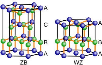
In polytypical NWs, the common growth direction is the ZB [111], which exhibit a noticeable similarity to WZ [0001]. Actually, analyzing both crystal structures in these directions, one can describe then as stacked hexagonal layers. The ZB has three layers in the stacking sequence (ABCABC) while WZ has only two (ABAB) as shown in Figure 1. The crystal structure alternation occurs when a stacking fault happens in WZ, leading to a single ZB segment, or when two twin planes appear in ZB, originating a single WZ segment naturenano-4-50 .
II.2 B. Irreducible representations at the polytypical interface
An important issue of the model is how to connect the energy levels at the polytypical interface depending on the symmetry they assume. Based on the scheme presented by Murayama and Nakayama prb-49-4710 of single group IRs at the WZ/ZB interface the symmetry of the energy bands can be chose. The same scheme was constructed by De and Pryor prb-81-155210 for the double group IRs with the inclusion of the spin-orbit coupling.
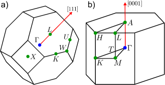
Since WZ has twice more atoms in the primitive unit cell than ZB, the number of energy bands in the -point is also twice as large. Considering the hybridization, without spin, ZB has 8 energy bands while WZ has 16. However, in the [111] direction, the ZB unit cell is two times larger than the usual face-centered cubic (FCC) unit cell prb-49-4710 . In the IRs scheme mentioned above, the presence of energy bands with symmetry takes into account the mismatch in the number of atoms for the usual unit cells. The reason for the appearance of the symmetry is the fact that ZB [111] growth direction is directed towards the -point, as displayed in Figure 2a, hence this point is mapped out in the -point. Figure 2b, displays the first Brillouin zone (FBZ) for the WZ structure.
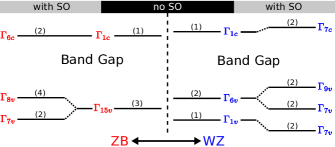
Among all the IRs presented in Refs. prb-49-4710 ; prb-81-155210 we considered only a small subset. Displayed in Figure 3, this subset comprises the lower conduction band and the top three valence bands, which belong to the -point in both structures. The price that is paid in considering only a small subset is the accuracy of the Hamiltonian for a fraction of the FBZ, approximately 10-20%. The basis states for the IRs of the considered bands are presented in equations (1) and (2) for ZB and WZ, respectively.
| (1) |
| (2) |
Although the IRs belong to different symmetry groups ( and ), the basis states transform as the usual cartesian coordinates for the valence bands and the scalar for the conduction band in both crystal structures. This information is crucial to represent WZ and ZB with the same Hamiltonian and is the essential insight of our formulation.
III III. Theoretical model
III.1 A. kp Hamiltonian
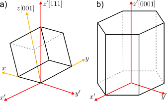
In order to develop our kp Hamiltonian arxiv it is convenient to describe the ZB structure in a coordinate system that has the axis parallel to the growth direction. This coordinate system is the primed one presented in Figure 4. Even though the choice of the coordinate system is arbitrary, it alters the kp Hamiltonian. For example, in the unprimed coordinate system the direction is directed towards the -point but in the primed coordinate system it is directed towards the -point. Thus our expectation is that an anisotropy in the ZB Hamiltonian between the and directions will occur since they are not reaching equivalent points in the the reciprocal space anymore.
Considering the single group formulation of the kp method, the choice of the coordinate system defines the symmetry operation matrices used to derive the momentum matrix elements. It is necessary to recalculate the Hamiltonian terms for the ZB structure. However, the energy bands we consider here are exactly the ones customary used in the ZB [001] kp Hamiltonian. Instead of recalculating the terms for ZB [111] kp Hamiltonian it is possible, and also useful, to apply a basis rotation to the ZB [001] matrix. This rotation procedure is well described in the paper of Park and Chuang jap-87-353 .
The basis set for both crystal structures in the primed coordinate system (the prime will be dropped out of the notation from now on and will be used only when it is necessary) is given by
| (3) |
In a first approximation, the interband interaction is not taken into account explicitly here, thus the conduction band is a single band model for spin-up and spin-down reading as
| (4) |
where is the band gap, is the energy reference at and , are the electron effective masses parallel and perpendicular do the axis, respectively. For the ZB structure, however, the electron effective masses are equal.
The Hamiltonian for WZ and ZB valence band is given by
| (5) |
and the matrix terms are defined as
| (6) |
where are the wave vectors in the primed coordinate system, are the holes effective mass parameters, is the crystal field splitting energy in WZ, are the spin-orbit coupling splitting energies and .
It is important to notice that the parameter appears in the matrix elements to regain the original isotropic symmetry of the ZB band structure in the new coordinate system. In the regions of WZ crystal structure, this parameter is zero and the matrix is exactly the canonical in use for WZ crystals.
Although this is not the usual way to describe ZB crystals, all the parameters in the matrix can be related to the familiar and as shown above
| (7) |
One may also argue that this formulation is very similar to the WZ phase. The insight here is to consider ZB as a WZ structure without the crystal field splitting energy. Since the WZ structure is less symmetric than ZB, as mentioned in section II.A, it is possible to represent the ZB parameters with the WZ ones.
The resulting valence band structures for bulk WZ and ZB InP using matrix (5) are shown in Figure 5. The presence of the crystal field in the WZ structure creates three distinct two-fold degenerate bands whereas in ZB there is a four-fold and a two-fold degenerate set of bands. Additionally, the anisotropy between and is evident in both crystal structures. In WZ it is due to the different symmetry properties of the -plane and the axis but in ZB it is because and directions do not reach equivalent points in the reciprocal space. Since the conduction band is a parabolic model, we did not present its dispersion relation. The ZB parameters were obtained from Ref. jap-89-5815 and the WZ parameters were derived using the effective masses presented in Ref. prb-81-155210 . These parameters can be found in Table LABEL:tab:kp_par.
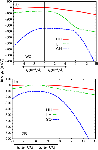
Following Chuang and Chang apl-68-1657 notation, the valence energy bands for WZ are named after the composition of the states at . HH (heavy hole) states are composed only by or , LH (light hole) states are composed mainly of or and CH (crystal-field split-off hole) are composed mainly of or . For the ZB structure the common identification of the valence energy bands was used. The four-fold degenerate bands at are HH and LH and the lower two-fold degenerate band is SO (split-off hole).
| Parameter | ZB InP | WZ InP |
|---|---|---|
| Lattice constant (Å) | ||
| 5.8697 | 4.1505 | |
| - | 6.7777 | |
| Energy parameters (eV) | ||
| 1.4236 | 1.474 | |
| 0 | 0.303 | |
| 0.036 | 0.036 | |
| Conduction band effective masses | ||
| 0.0795 | 0.105 | |
| 0.0795 | 0.088 | |
| Valence band effective mass | ||
| parameters (units of ) | ||
| -13.4800 | -10.7156 | |
| -0.8800 | -0.8299 | |
| 12.6000 | 9.9301 | |
| -6.3000 | -5.2933 | |
| -5.8000 | 5.0000 | |
| -7.4953 | 1.5000 | |
| -0.5000 | 0 |
III.2 B. Strain
The strain Hamiltonian can be obtained using the same basis rotation applied to the kp matrix jap-87-353 . Similarly, the conduction and valence band are decoupled.
For the conduction band, the strain effect is given by
| (8) |
where and are the conduction band deformation potentials parallel and perpendicular to the axis, respectively. In the ZB structure they have the same value.
The valence band strain Hamiltonian is
| (9) |
and the matrix terms are
| (10) |
where ’s are the valence band deformation potentials and is the strain tensor.
In the same way as the parameter appears in kp matrix, some extra deformation potential terms were appears to use the same strain Hamiltonian for both crystal structures. The deformation potential was split in two parts because the strain tensor is not present in the ZB structure. For WZ, . Also, the deformation potential takes into account the non existing term in the WZ structure.
The deformation potentials ’s are related to the ZB ones
| (11) |
Considering biaxial strain, the elements of the strain tensor can be obtained in both coordinate systems for ZB and WZ. Although it is convenient to describe the Hamiltonian terms in the primed coordinate system, it is also useful to describe the strain tensor elements in the unprimed coordinate system. They will be used to construct the piezoelectric polarization in section III.C. The prime will be reintegrated in the notation to avoid confusion and the upper scripts and denotes the ZB and WZ structures, respectively.
For the primed coordinate system, the elements of the strain tensor are given by
| (12) |
| (13) |
| (14) |
| (15) |
where is the lattice constant of the substrate.
In the unprimed coordinate system, the strain tensor elements assume the form
| (16) |
| (17) |
The quantity is given by
| (18) |
Comparing the expression (13) with (14) it is possible to obtain effective values for and for ZB in the primed coordinate system. The effective values are:
| (19) |
| (20) |
Thus, we have a single set of expressions to describe biaxial strain in the primed coordinate system for ZB and WZ crystal structures:
| (21) |
| (22) |
| (23) |
Since deformation potentials and elastic stiffness constants for WZ InP are not yet available in the literature, we will consider here that the strain effect appears only in the ZB structure. This assumption is not totally unrealistic because WZ is the dominant phase in the NW.
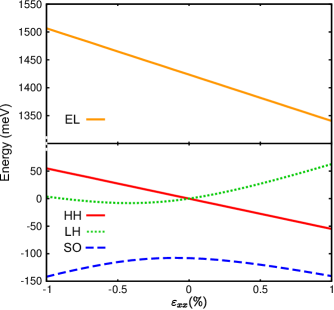
Figure 6 shows the effect of strain at for the diagonalized Hamiltonian (kp and strain terms) as a function of the percentage of strain tensor. A linear variation for the conduction band and the HH band is observed, however, the LH and SO bands have a non-linear behavior. The order of the HH and LH bands changes when strain is distensive. Table LABEL:tab:strain_par lists the ZB parameters used in the calculations.
| Parameter | ZB InP |
|---|---|
| Deformation potentials (eV) | |
| -6.3735 | |
| 2.2868 | |
| 8.6603 | |
| -4.3301 | |
| 3.8868 | |
| 0 | |
| 0 | |
| -0.4434 | |
| -6.0 | |
| -6.0 | |
| Elastic stiffness constant (GPa) | |
| 1011 | |
| 561 | |
| 456 |
III.3 C. Spontaneous and Piezoelectric Polarization
Piezoelectric polarization appears when a crystal is subjected to strain. In ZB semiconductors grown along the [111] direction, the magnitude of the piezoelectric polarization, in the unprimed coordinate system of Fig. 4, is given by prb-35-1242 :
| (24) |
where is the piezoelectric constant for ZB materials, are the cartesian coordinates in a cyclic order and are the strain tensor components.
Applying the coordinate system rotation in the piezoelectric polarization vector components in order to describe them in the primed coordinate system we obtain:
| (25) |
The resulting piezoelectric polarization alongside the growth direction is then:
| (26) |
The spontaneous polarization effect in WZ structure is due to the relative displacement between the cations and anions when the ratio is different from the ideal value in the WZ structure.
In a heterostructure, the effect of the different polarizations in each region creates an electric field through the whole structure. The net electric field in a determined layer, , due to spontaneous and piezoelectric polarizations in the system is given by paul-harrison :
| (27) |
where sums all over the layers in the heterostructure with polarization , dielectric constant and length .
III.4 D. Effective mass equation in reciprocal space
The envelope function approximation book-bastard ; IEEEjqe-22-1625 is applied to couple the different crystal structures alongside the growth direction in the NW. In each region the wave function is expanded in terms of the Bloch functions of the corresponding polytype. Thus, the wave function of the whole system is given by:
| (28) |
where are the envelope functions of the -th basis state.
Considering different Bloch functions for each region, the Hamiltonian parameters vary alongside the growth direction, making it possible to use the common kp and strain matrices, (5) and (9), for both crystal structures. Moreover, since each crystal structure dictates its symmetry to their respective Bloch functions, some matrix elements can be forbidden by symmetry in the region of a certain crystalline phase. For example, the parameter is zero in WZ regions whereas the parameter is zero in ZB regions.
To represent the growth dependence of the Hamiltonian parameters and envelope functions, the plane wave expansion is used. This formalism considers the periodicity of the whole system allowing the expansion of growth dependent functions in Fourier coefficients:
| (29) |
where are the Fourier coefficients of the function and is a reciprocal lattice vector. The Fourier expansion also induces the change in the kp matrix.
IV IV. Results and discussion
The NW system chosen to apply our model is a WZ/ZB/WZ single well structure. Although a real NW is composed of multiple polytypical quantum wells with different sizes, the analysis of just a single well can bring out the physics of the polytypical interface. The effects of lateral confinement are neglected in a first approach, assuming NWs with large lateral dimensions. Strain, piezoelectric and spontaneous polarization are also included in the single well system.
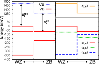
When both crystal structures are put side by side, a band-offset is created at the interface, originating a confinement profile. The band mismatch is also taken from reference prb-81-155210 . Figure 7 exhibits the WZ/ZB interface for InP in two different schemes: in the left, the energies in for the diagonalized Hamiltonian and in the right, the diagonal terms of the Hamiltonian. Although the composition of the states in the diagonalized energy bands are the same in , the matrix is not constructed in this basis. Since the variation along the growth direction of the matrix elements is well defined, the scheme in the right is more convenient to analyze the potential profile of the system.
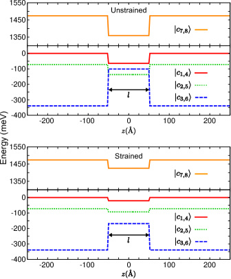
In all performed calculations, the entire length of the system is set to and the width of the ZB region, , is variable. Figure 8 shows the single well potentials with and without the effect of strain. Since the potential profiles exhibits a type-II behavior, we expect a spatial separation of the carriers: electrons are more likely to be in the ZB region and the holes in the WZ region.
The strain considered here, , is a intermediate value between two data available in the literature from ab initio calculations. Reference ssc-151-781 shows that the deviation between the lattice constant of ZB[111] and WZ[0001] is and reference nanotec-21-505709 shows . Also, reference nanolet-10-4055 suggests a difference slighter than between the lattice constants of the two polytypes. The effect of strain shallows the potential wells in the conduction and valence bands, reducing the confinement of the carriers. We expect to have less confined states for the strained potential compared to the unstrained one.
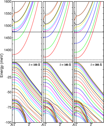
The conduction and valence band structures for the potential profile without strain are presented in Fig. 9 for three different widths of the ZB region. The calculations were performed up to 10% in the direction and 100% in the direction. For the valence band 64 energy states are presented while only 18 are presented for the conduction band. Since the system has no asymmetric potential, the energy bands are two-fold degenerate in spin, therefore 32 states are visible in the valence band and 9 in the conduction band. For the three different values of , the conduction energy bands are nominated, from bottom to top, as EL1-EL9, composed of states. The valence bands, from top to bottom, are nominated as HH1-19, LH1-4, HH20-21, LH5-7, HH22-23, LH8-9 for ; HH1-16, LH1-2, HH17, LH3, HH18, LH4, HH19, LH5-7, HH20-21, LH8-9, HH22-23 for and HH1-14, LH1-2, HH15, LH3, HH16-17, LH4-5, HH18, LH6, HH19, LH7, HH20, LH8, HH21, LH9, HH22, LH10 for .
Since the highest valence band states are HH there is no significant anticrossing among the energy bands in the direction. The anticrossing is characteristic of interactions between HH and LH bands in ZB and WZ quantum well structures. A slight anticrossing, however, can be seen in the energy region just above , which is next to the interaction region of the and profiles.
Increasing the value of we find that the number of confined states in the conduction band increases. On the other hand, for the valence band the number of confined states decreases because the WZ region’s width also decreases.
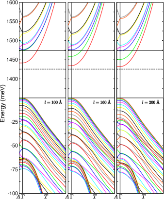
For the strained potential profile, the band structures for three different widths of the ZB region are displayed in Figure 10. The calculations were performed considering the same extension for the FBZ of the unstrained band structure. For the three different values of , the conduction energy bands are nominated, from bottom to top, as EL1-EL9, composed of states. The valence bands, from top to bottom, are nominated as HH1-22, LH1, HH23, LH2-7, HH24-25 for ; HH1-21, LH1-3, HH22-23, LH4-8, HH24 for and HH1-21, LH1-4, HH22-23, LH5-9 for .
As expected, the number of confined states for the strained profile compared to the unstrained one is smaller. Nonetheless, the similar confinement trend is visible here when the value of increases: the number confined states in the conduction band increases while in valence band decreases.
An interesting feature presented in the strained band structure is the presence of some confined states below the top region, around . This suggests a confinement in the intermediate region of the and profiles. Note that the coupling of these two profiles at happens because of the off-diagonal spin-orbit term.
The composition of the energy states at in the band structure is similar for the strained and unstrained cases: they are just HH or LH states. There is no CH states in the energy range considered here. The major contribution for CH states comes from the profile, which is the lowest one in both cases.
The information of the energy states’ composition can reveal important trends in the luminescence spectra for this kind of system. For example, at the dominant symmetry of the energy states belongs to , which means that the luminescence spectra is more intense perpendicular to the growth direction. However, experimental measurements prb-82-125327 indicates that the intensities perpendicular and parallel to the growth direction are almost similar. Therefore, we expect that the contribution for the parallel luminescence comes from the states at . For points away from the -point, there is a stronger mixing between all the basis states.
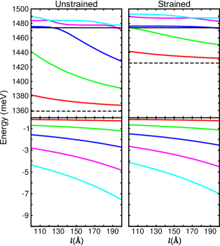
The effect of the ZB region width for both strained and unstrained potential profile for the conduction and valence band states at is presented in Figure 11. It is possible to observe that the number of confined states in the conduction band increases as the value of increases. On the other hand, the number of confined states in the valence band decreases. Nevertheless, the effect of the variation of is more significant for the conduction band since the electron effective mass in ZB () is smaller than the heavy hole mass of WZ ( and ). The same trend is also observed in the strained case. Also, since the bottom of the well in the conduction band has a higher value in the strained case, we can expect the interband transition energies to be blueshifted with the inclusion of strain effects.
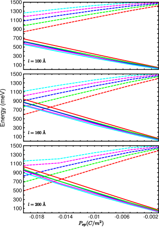
The presence of strain effects gives rise to the piezoelectric polarization. For the InP ZB, the value for the piezoelectric constant used was , taken from Ref. jap-92-932 . For both crystal structures, the value used for static dielectric constant was . The unknown parameter is the spontaneous polarization for WZ InP. Ref. nanolet-10-4055 suggests that this value is smaller than that of InN (). In an attempt to estimate this value for InP, we performed the band structure calculations considering a range of values for .
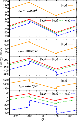
The energy of the first 5 conduction and valence band states at as a function of spontaneous polarization in WZ InP for three different ZB region widths is presented in Figure 12. The considered values for spontaneous polarization are , , , and . For and there is a crossing between the conduction and valence band states. This is not observed experimentally therefore we consider this region forbidden. Then, the allowed values for spontaneous polarization considered here are then , and .
The diagonal potential profile including effects of piezoelectric and spontaneous polarization is presented in Figure 13. The ZB region is fixed at . Analyzing these profiles, we expect to have strong coupling in the band structure for higher values of since the profiles are more close to each other. This induces the mixing of states because an energy value can be in more than one profile.
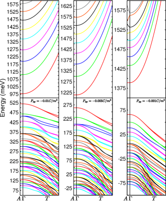
The resulting band structures for the three different potential profiles of Figure 13 are shown in Figure 14. For the three different values of , the conduction energy bands are nominated, from bottom to top, as EL1-EL9, composed of states. The valence bands, from top to bottom, are nominated as HH1-2, LH1, HH3, LH2, HH4-5, LH3, HH6, LH4, HH7, LH5, HH8, LH6, HH9, LH7, HH10, LH8, HH11, LH9, HH12, LH10, HH13, LH11, HH14, LH12, HH15, LH13, HH16, LH14, HH17, LH15 for ; HH1-3, LH1, HH4, LH2, HH5-6, LH3, HH7, LH4, HH8, LH5, HH9-10, LH6, HH11, LH7, HH12, LH8, HH13, LH9, HH14, LH10, HH15-16, LH11, HH17, LH12-13, HH18, LH14 for and HH1-7, LH1, HH8-9, LH2, HH10-11, LH3, HH12-13, LH4, HH14-15, LH5, HH16, LH6, HH17-18, LH7, HH19, LH8, HH20, LH9, HH21-22, LH10 for . The number of HH states increases as the value of decreases.
The anticrossings and also the spin splitting in the valence sub bands are more visible for higher values of . The strength of the resulting electric field not only increases the mixing of HH and LH states but also increases the value of the spin splitting in each sub band. This spin splitting is known as the Rashba effect jpc-17-6039 and is due to potential inversion asymmetry, even though the term does not appear explicitly in the Hamiltonian book-winkler .
The number of confined states decreases as the spontaneous polarization decreases. On the other hand, the energy difference between the conduction and valence band ground state increases as the spontaneous polarization decreases, blueshifting the interband energy transitions.
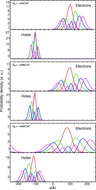
The effect of piezoelectric and spontaneous polarization also induce carriers’ spatial separation. This effect, in the probability densities in can be seen in Fig. 15. The lowest four states of the conduction band and the highest four states of the valence band are presented. At the wave functions of spin-up and spin-down are degenerated. We can see that the overlap increases for more excited states, also blueshifting the energy peak in the interband transitions. Since the potential profile is not completely even or odd, the envelope functions no longer have well defined parities.
V V. Conclusions
The basic result of this study is the theoretical model based on the kp method and group theory concepts to calculate band structures of WZ/ZB polytypical systems in the vicinity of the band edge. The method allows us to describe in the same matrix Hamiltonian the ZB and WZ structures, with along the [111] and [0001] directions, respectively. Since the WZ structure is less symmetric, the ZB parameters are assigned to the WZ ones. Our method not only is able to describe the kp terms of the Hamiltonian but also includes the strain and polarization (spontaneous and piezoelectric) effects.
Extracting the parameters of WZ InP from Ref. prb-81-155210 we applied our model to a WZ/ZB/WZ single well in order to understand the physics of the polytypical interface. The potential profile at the interface WZ/ZB is type-II, whose feature is the spatial separation of carriers. The performed calculations in this study holds this characteristic.
Due to the lack of parameters in the literature for WZ InP, only the strain effect in the ZB region was considered here. This seems to be a reasonable consideration since the WZ structure is the dominant phase in NWs structures. However, such strain parameters would be fundamental in a system that the stable lattice constant is a intermediate value between WZ and ZB InP lattice parameters.
Within the limitation of strain, the piezoelectric polarization was also considered in the ZB region. For the WZ region, only the spontaneous polarization appears. Since there is no value in the literature for the spontaneous polarization of WZ InP, a range of values were considered in the simulations. Some of these values, however, induces a negative gap in the system. There is no data in the literature that corroborates this effect.
The proposed model, jointly with the obtained results, proved to be useful in the study of electronic band structures of WZ/ZB polytypical systems, such as NWs. Exploring the opportunities of band gap engineering considering not only different compounds, but also different crystal structures, could lead to the development of novel nanodevices.
VI Acknowledgements
The authors acknowledge financial support from the Brazilian funding agencies CAPES and CNPq.
References
- (1) Y. Cui, Q. Wei, H. Park, and C. M. Lieber, Science 293, 1289 (2001)
- (2) F. Patolsky, G. Zheng, and L. C. M., Nanomedicine 1, 51 (2006)
- (3) G. Zheng, F. Patolsky, Y. Cui, W. U. Wang, and C. M. Lieber, Nature Biotechnology 23, 1294 (2005)
- (4) X. Duan, Y. Huang, R. Agarwal, and C. M. Lieber, Nature 421, 241 (2003)
- (5) X. Duan, Y. Huang, Y. Cui, J. Wang, and C. M. Lieber, Nature 409, 66 (2003)
- (6) H. Ng, J. Han, T. Yamada, and P. Nguyen, Nano Letters 4, 1247 (2004)
- (7) R. S. Wagner and W. C. Ellis, Applied Physics Letters 4, 89 (1964)
- (8) V. Dubrovskii, G. Cirlin, and V. Ustinov, Semiconductors 43, 1539 (2009)
- (9) Y. Kitauchi, Y. Kobayashi, K. Tomioka, S. Hara, K. Hiruma, T. Fukui, and J. Motohisa, Nano Letters 10, 1699 (2010)
- (10) J. Johansson, L. S. Karlsson, C. P. T. Svensson, T. Mårtensson, B. A. Wacaser, K. Deppert, L. Samuelson, and W. Seifert, Nature Materials 5, 574 (2005)
- (11) P. Caroff, K. A. Dick, J. Johansson, M. E. Messing, K. Deppert, and L. Samuelson, Nature Nanotechnology 4, 50 (2009)
- (12) S.-G. Ihn, J.-I. Song, Y.-H. Kim, J. Y. Lee, and I.-H. Ahn, IEEE Transactions on Nanotechnology 6, 384 (2007)
- (13) J. Bao, D. C. Bell, F. Capasso, N. Erdman, D. Wei, L. Fröberg, T. Mårtensson, and L. Samuelson, Advanced Materials 21, 3654 (2009)
- (14) J. Bolinsson, P. Caroff, B. Mandl, and K. A. Dick, Nanotechnology 22, 265606 (2011)
- (15) C. Thelander, P. Caroff, S. Plissard, A. W. Dey, and K. A. Dick, Nano Letters 11, 2424 (2011)
- (16) K. A. Dick, P. Caroff, J. Bolinsson, M. E. Messing, J. Johansson, K. Deppert, L. R. Wallenberg, and L. Samuelson, Semiconductor Science and Technology 25, 024009 (2010)
- (17) G. Dresselhaus, Physical Review 100, 580 (1955)
- (18) E. O. Kane, Physics of III-V compounds, Semiconductors and Semimetals, Vol. 1 (Academic Press, New York, 1966)
- (19) G. E. Pikus, Soviet Physics JETP 14, 898 (1962)
- (20) G. Bir and G. Pikus, Symmetry and strain-induced effects in semiconductors (Wiley, New York, 1974)
- (21) S. L. Chuang and C. S. Chang, Physical Review B 54, 2491 (1996)
- (22) G. Bastard and J. A. Brum, IEEE Journal of Quantum Electronics 22, 1625 (1986)
- (23) G. M. Sipahi, R. Enderlein, L. M. R. Scolfaro, and J. R. Leite, Physical Review B 53, 9930 (1996)
- (24) S. C. P. Rodrigues, G. M. Sipahi, L. M. R. Scolfaro, and J. R. Leite, Applied Physics Letters 76, 1015 (2000)
- (25) L. C. Chuang and C. S. Chang, Semiconductor Science and Technology 12, 252 (1997)
- (26) S. C. P. Rodrigues and G. M. Sipahi, Journal of Crystal Growth 246, 347 (2002)
- (27) M. Murayama and T. Nakayama, Physical Review B 49, 4710 (1994)
- (28) A. De and C. E. Pryor, Physical Review B 81, 155210 (2010)
- (29) K. Pemasiri, M. Montazeri, R. Gass, L. M. Smith, H. E. Jackson, J. Yarrison-Rice, S. Paiman, Q. Gao, H. H. Tan, C. Jagadish, X. Zhang, and J. Zou, Nano Letters 9, 648 (2009)
- (30) S. Paiman, Q. Gao, H. H. Tan, C. Jagadish, K. Pemasiri, M. Montazeri, H. E. Jackson, L. M. Smith, J. M. Yarrison-Rice, X. Zhang, and J. Zou, Nanotechnology 20, 225606 (2009)
- (31) E. G. Gadret, G. O. Dias, L. C. O. Dacal, M. M. de Lima Jr., C. V. R. S. Ruffo, F. Iikawa, M. J. S. P. Brasil, T. Chiaramonte, M. A. Cotta, L. H. G. Tizei, D. Ugarte, and A. Cantarero, Physical Review B 82, 125327 (2010)
- (32) L. Zhang, J.-W. Luo, A. Zunger, N. Akopian, V. Zwiller, and J.-C. Harmand, Nanoletters 10, 4055 (2010)
- (33) D. Li, Z. Wang, and F. Gao, Nanotechnology 21, 505709 (2010)
- (34) L. C. O. Dacal and A. Cantarero, Solid State Communications 151, 781 (2011)
- (35) M. Moewe, L. C. Chuang, V. G. Dubrovskii, and C. Chang-Hasnain, Journal of Applied Physics 104, 044313 (2008)
- (36) M. S. Dresselhaus, G. Dresselhaus, and A. Jorio, Group Theory: application to the physics of condensed matter (Springer-Verlag, 2008)
- (37) P. E. Faria Junior and G. M. Sipahi, http://arxiv.org/abs/1012.0227(2010)
- (38) S. H. Park and S. L. Chuang, Journal of Applied Physics 87, 353 (2000)
- (39) I. Vurgaftman, J. R. Meyer, and L. R. Ram-Mohan, Journal of Applied Physics 89, 5815 (2001)
- (40) S. L. Chuang and C. S. Chang, Applied Physics Letters 68, 1657 (1996)
- (41) C. Mailhiot and D. L. Smith, Physical Review B 35, 1242 (1987)
- (42) P. Harrison, Quantum Wells, Wires and Dots: Theoretical and Computational Physics of Semiconductor Nanostructures (John Wiley and Sons Ltd, 2006)
- (43) G. Bastard, Wave mechanics applied to semiconductor heterostructures (Halsted Press, Les Ulis Cedex, France, 1988)
- (44) H. Magnus, M. E. Pistol, and C. Pryor, Journal of Applied Physics 92, 932 (2002)
- (45) Y. A. Bychkov and E. I. Rashba, Journal of Physics C: Solid State Physics 17, 6039 (1984)
- (46) R. Winkler, Spin-orbit coupling effects in two-dimensional electron and hole systems (Springer, Berlin, 2003)