Polarization-sensitive absorption of THz radiation by interacting electrons in chirally stacked multilayer graphene
Abstract
We show that opacity of a clean multilayer graphene flake depends on the helicity of the circular polarized electromagnetic radiation. The effect can be understood in terms of the pseudospin selection rules for the interband optical transitions in the presence of exchange electron-electron interactions which alter the pseudospin texture in momentum space. The interactions described within a semi-analytical Hartree–Fock approach lead to the formation of the topologically different broken–symmetry states characterized by Chern numbers and zero-field anomalous Hall conductivities.
I Introduction
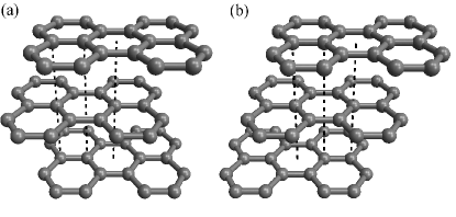
Multilayer graphene is a link between one atom thick carbon layersNovoselov et al. (2005) with the peculiar Dirac-like effective Hamiltonian for carriersCastro Neto et al. (2009) and graphiteWallace (1947) which can be seen as millions of graphene layers stacked together. Graphene layers placed together do not lie exactly one on top of each other but are shifted in such a way that only half of the carbon atoms have a neighbor in another layer and the other half are projected right into the middle of the graphene’s “honeycomb cell”. If the third layer aligns with the first (and the layer with the -th) then we arrive at the more stable arrangement of graphene layers known as Bernal (or AB) stacking, see Fig. 1a. However, this is not the only possible configuration. One can imagine an alternative stacking when the third layer aligns neither the first nor the second but shifted with respect to both, see Fig. 1b. This arrangement is known as rhombohedral (or ABC) stacking and represents the main topic of this work.
The very first studies of Bernal and rhombohedral graphitesWallace (1947); McClure (1957); Slonczewski and Weiss (1958); Haering (1958); McClure (1969) relying on the tight binding model have demonstrated the strong dependence of the band structure on the stacking order. Later on the progress in numerical methods made it possible to refine the tight binding model outcomes using ab initio calculations Painter and Ellis (1970); Tománek and Louie (1988); Charlier et al. (1991). The seminal transport measurements on grapheneNovoselov et al. (2004) have inspired recent investigationsLatil and Henrard (2006); Partoens and Peeters (2006, 2007); Guinea et al. (2006); Avetisyan et al. (2010) of the band structure in a few layer graphene having different stacking patterns. The band structure demonstrates a large variety of behavior including a gapless spectrum, direct and indirect band gaps, and energetic overlap of the conduction and valence bands even though the number of layers has been limited by four.Latil and Henrard (2006) Note that the band gap can be induced by an external electric field. Avetisyan et al. (2010) The influence of an external magentic field (Landau levels) has also extensively been studied. Guinea et al. (2006); Yuan et al. (2011a); Taychatanapat et al. (2011) The electron-electron interactions have been taken into account in Refs. Yuan et al. (2011b); Zhang et al. (2010a, 2011); Nandkishore and Levitov (2010); 2012lemonik (201), also including the Zeeman term. Zhang and MacDonald (2011) There are experimental indications that electron-electron interaction effects play an important role in a few layer graphene where charge carriers may exhibit a variety of broken symmetry states. Weitz et al. (2010); Bao et al. (2011); Velasco et al. (2012); Mayorov et al. (2011)
The brief literature overview given above illustrates how rich the band structure of multilayer graphene (and the effects associated with) can be. Note, however, that among all stacking possibilities, only the pure ABC arrangement maintains the sublattice pseudospin chirality. Zhang et al. (2010b) In the simplest case of negligible interlayer asymmetries and trigonal warp the simplified two-band ABC graphene model leads to the following Hamiltonian close to the neutrality pointZhang et al. (2010b)
| (1) |
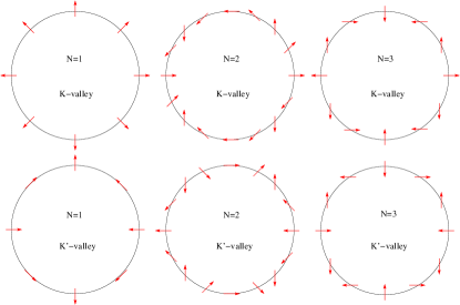
where is the group velocity for carriers in single layer graphene, is the hopping parameter, is the valley index, and is the number of layers. As one can see from Eq. (1), the N-layer and (N+1)-layer graphene stacks differ, apart from the density of states, by only the winding number associated with the pseudospin orientation. The pseudospin texture in the momentum space associated with Hamiltonian (1) and shown in Fig. 2 is the main topic of this work. In what follows we focus on the influence of electron-electron exchange interactions on the pseudospin texture and its detection by optical means.
Note that the pseudospin lies in the -plane as long as its carrier remains in an eigenstate of . The exchange interactions can turn the pseudospin texture to the out-of-plane phase with the out-of-plane angle depending on the absolute value of the particle momentum Trushin and Schliemann (2011); Zhang et al. (2011); Jung et al. (2011); Min et al. (2008). This is due to the huge negative contribution to the Hartree–Fock ground state energy from the valence band (i. e. “antiparticle” states) which cannot be neglected in graphene because of the zero gap and conduction-valence band coupling via pseudospin. The broken symmetry states in multilayer graphene with chiral stacking have been recently studied by Zhang et al Zhang et al. (2011) using quite general arguments. Spontaneous symmetry breaking can occur in presence of exchange electron-electron interactions Min et al. (2008). Here, we utilize a simplified model which includes exchange electron-electron interactions but, at the same time, allows transparent half-analytical solution. Having this solution at hand we focus on the manifestation of such broken symmetry states in optical absorption measurements.
Optical absorption via the direct interband optical transitions in monolayer graphene has been investigated in Nair et al. (2008) and shown to be equal to the universal value . In the presence of the electron-electron interactions the interband absorption can be substantially reduced or enhanced as compared to its universal value just by switching the helicity of the circularly polarized light Trushin and Schliemann (2011). This effect is due to the peculiar pseudospin texture arising from the interplay between pseudospin-momentum coupling and exchange interactions. To observe the pseudospin texture in chirally stacked multilayer graphene by optical means the photon energy must be much smaller than the bottom of the lowest split-off bands . To give an example, a laser Karch et al. (2008) with wavelength (i.e. with the photon energy ) safely satisfies this condition.
II Model
We start from the Coulomb exchange Hamiltonian for chiral carriers which is given by
| (2) |
with and being the band index with for the conduction band. In order to consider the exchange Hamiltonian for any on the equal footing we assume strictly two-dimensional Fourier transform for Coulomb potential. This is in contrast to Min et al. (2008) where the interlayer distance has been included in the screening multiplier . Since the wave vector difference can not be larger than the momentum cut-off of the order of employed in our model (see below) the screening multiplier is always of the order of and can be disregarded here. The intervalley overlap is also assumed to be negligible, and the eigenstates of can be formulated as with spinors , , and , where a non-zero out-of-plane pseudospin component corresponds to . To diagonalize the following -independent equation for must be satisfied Juri and Tamborenea (2008); Trushin and Schliemann (2011)
| (3) |
Here the integration goes over the occupied states. Note that the conduction and valence states are entangled, and the latter cannot be disregarded even at positive Fermi energies assumed below. Thus, in order to evaluate the integrals in Eq. (3) a momentum cut-off is necessary. Most natural choice corresponds to the energy scale at which the split-off bands of bilayer graphene become relevant and our two-band model no longer applies. Substituting we arrive at
| (4) | |||
where . The momentum cut-off is assumed to be much larger than the Fermi momentum , and, therefore, we can set the lower integral limit to zero. In this case our outcomes do not depend on the value of .


Besides a trivial solution with independent of , there are non-trivial ones and with shown in Figs. 3a and 4a for different and . The solutions and represent to two phases with different total ground state energies () for the in-plane (out-of-plane) pseudospin phase. The difference per volume is given by
| (5) |
The ground state energy is the same for both valleys and spins, and, therefore, Eq. (5) contain and for spin and valley degeneracy respectively. has been evaluated numerically and the resulting vs. dependency is shown in Figs. 3b and 4b for suspended and -placed graphene respectively. One can see that strong electron-electron interactions with definitely make the out-of-plane phase energetically preferable for . For graphene placed on substrate the pseudospin out-of-plane phase is energetically preferable only for . Note that the estimates of for clean monoatomic graphene flake vary from (Ref. Jang et al. (2008)) to (Ref. Peres et al. (2005)) and, therefore, even monolayer graphene may get to the pseudospin out-of-plane phase.


Note that it is possible to choose either the same or opposite solutions for two valleys. The former choice breaks the parity invariance whereas the latter one does so with the time reversal symmetry.Trushin and Schliemann (2011) In what follows we consider possible manifestations of these solutions in the optical absorption measurements on multilayer graphene.
III Optical absorption
We assume that an electromagnetic wave is propagating along axis perpendicular to graphene plane. It can be described by the electric field , where is the wave vector, and is the radiation frequency. For our purpose it is more convenient to characterize the electromagnetic wave by its vector potential , where . The relation between and is unambiguous since is always in plane resulting in a gauge with . The interaction Hamiltonian can be then written in the lowest order in as
| (6) | |||
| (9) |
The total absorption can be calculated as a ratio between the total electromagnetic power absorbed by graphene per unit square and the incident energy flux . The probability to excite an electron from the valence band to an unoccupied state in the conduction band can be calculated using Fermi’s golden-rule
Because of normal incidence there is zero momentum transfer from photons to electrons. What is important is that the inter-band transition matrix elements of turn out to be sensitive to the light polarization and pseudospin orientations in the initial and final states. In particular, for linear polarization with and the probability to excite an electron with a given momentum reads
| (10) |
Note that does not depend on the valley index . The total optical absorption is not sensitive to the particular orientation of the polarization plane since the -dependent term is integrated out in this case. In contrast, if we assume a circular polarization fulfilling , then the interband transition probability for K-valley can be written as
| (13) |
Here, the multipliers and are for two opposite helicities of light, and for K’-valley they are interchanged. If the out-of-plane pseudospin polarization is chosen to be opposite in two valleys then this helicity dependence survives the integration over momentum and summation over valley index resulting in the helicity-sensitive total absorption which reads
| (16) | |||
| (17) |
The absorption strongly depends on helicity as long as the radiation frequency is much smaller than the band split-off energy. This regime corresponds to the excitation of electrons with comparatively small momenta, where the angle is close to zero, see Fig. 3b and Fig. 4b. In the in-plane phase with the total absorption does not depend on light polarization, and in the non-interacting limit it equals to
| (18) |
At it acquires the universal value , as expectedNair et al. (2008).
The experiment proposed here is similar to the one discussed recently in Ref. Nandkishore and Levitov (2011) suggesting to detect broken symmetry states in graphene placed on substrate by polar Kerr rotation measurements, i.e. by analyzing the elliptical polarization of reflected radiation. In the present paper, however, we propose to reach the same goal by comparing the opacity for two orthogonal light polarizations, which appears to be the simpler strategy.
Alternatively, one can characterize broken–symmetry states in terms of the topological Chern numbers Thouless et al. (1982) given by
| (19) |
with . This approach is routinely used in the theory of topological insulators Hasan and Kane (2010) and originated from the description of quantized Hall conductances.
A non-trivial band topology has also been found in graphene Kane and Mele (2005); Prada et al. (2011) where the band gap was opened via spin-orbit coupling characterized just by a constant (i.e. wave vector independent) mass term rather than by exchange interactions described by a more complicated Hamiltonian (2).
Note, that in our case here contains a term proportional to which occurs due to the singularity in but does not contribute to as long as at . Thus, for the conduction band electrons we have
| (20) |
Assuming the out-of-plane pseudospin polarization to be opposite in two valleys it follows that the total Chern number for conduction electrons just equals . On the other hand, the total Chern number is zero as long as the out-of-plane pseudospin pseudospin component is same in both valleys. Thus, the two out-of-plane solutions are topologically different even though they correspond to the band gap of the same size. The topologically non-trivial case with corresponds to broken time reversal symmetry leading to the existence of a zero-field Hall current Trushin and Schliemann (2011).
The only question is whether the time reversal broken states really occur in clean graphene samples. More in depth analysis performed by Nandkishore and Levitov Nandkishore and Levitov (2011, 2010) suggests that this is the case at least for bilayer graphene. On the other hand Jung et al.Jung et al. (2011) demonstrate that the intervalley exchange coupling favors parallel pseudospin polarization in opposite valleys breaking the parity invariance. In this case the total absorption does not depend on the radiation helicity but the two valleys are occupied differently by the photoexcited carriers which might be useful effect for valleytronics Xiao et al. (2007). Note that the strain effects also may change the band structure topology in bilayer Mucha-Kruczyński et al. (2011) and probably multilayer graphene. This might be an issue in suspended samples where mechanical deformations can occur easily. There is, however, an experimental evidence Mayorov et al. (2011) of the fact that it is the electron-electron interaction rather than the strain that is responsible for the band structure reconstruction.
IV Conclusion
We have demonstrated that the polarization-sensitive optical absorption predicted in Trushin and Schliemann (2011) for single layer graphene can be found in chirally stacked carbon multilayers within a broader range of parameters. This is due to the enhancement of the interaction effects in multilayer graphene with larger number of layers. The conditions necessary for the observation of the polarization-dependent optical absorption can be summarized as follows. (i) Graphene samples must be prepared as cleaner as possible. It would be better to utilize suspended samples in order to isolate the interacting electrons from the environment with large relative permittivity. (ii) The exchange interactions must break the time reversal invariance rather than the parity. This situation corresponds to the topologically non-trivial state with the Chern number equal to . (iii) Finally, the low frequency radiation is necessary to excite the electrons with smaller momenta having larger out-of-plane pseudospin components and to preclude the influence of split-off bands.
In addition, we would like to mention the possible existence of a zero-field Hall current in the slightly doped graphene samples where the time reversal invariance is broken as described above.
Acknowledgements
We would like to thank Tobias Stauber, Jeil Jung, and Fan Zhang for stimulating discussions. This work was supported by DFG via GRK 1570.
References
References
- Novoselov et al. (2005) K. S. Novoselov, A. K. Geim, S. V. Morozov, D. Jiang, M. I. Katsnelson, I. V. Grigorieva, S. V. Dubonos, and A. A. Firsov, Nature 438, 197 (2005).
- Castro Neto et al. (2009) A. H. Castro Neto, F. Guinea, N. M. R. Peres, K. S. Novoselov, and A. K. Geim, Rev. Mod. Phys. 81, 109 (2009).
- Wallace (1947) P. R. Wallace, Phys. Rev. 71, 622 (1947).
- McClure (1957) J. W. McClure, Phys. Rev. 108, 612 (1957).
- Slonczewski and Weiss (1958) J. C. Slonczewski and P. R. Weiss, Phys. Rev. 109, 272 (1958).
- Haering (1958) R. R. Haering, Canadian Journal of Physics 36, 352 (1958).
- McClure (1969) J. W. McClure, Carbon 7, 425 (1969).
- Painter and Ellis (1970) G. S. Painter and D. E. Ellis, Phys. Rev. B 1, 4747 (1970).
- Tománek and Louie (1988) D. Tománek and S. G. Louie, Phys. Rev. B 37, 8327 (1988).
- Charlier et al. (1991) J.-C. Charlier, X. Gonze, and J.-P. Michenaud, Phys. Rev. B 43, 4579 (1991).
- Novoselov et al. (2004) K. S. Novoselov, A. K. Geim, S. V. Morozov, D. Jiang, Y. Zhang, S. V. Dubonos, I. V. Grigorieva, and A. A. Firsov, Science 306, 666 (2004).
- Latil and Henrard (2006) S. Latil and L. Henrard, Phys. Rev. Lett. 97, 036803 (2006).
- Partoens and Peeters (2006) B. Partoens and F. M. Peeters, Phys. Rev. B 74, 075404 (2006), URL http://link.aps.org/doi/10.1103/PhysRevB.74.075404.
- Partoens and Peeters (2007) B. Partoens and F. M. Peeters, Phys. Rev. B 75, 193402 (2007), URL http://link.aps.org/doi/10.1103/PhysRevB.75.193402.
- Guinea et al. (2006) F. Guinea, A. H. Castro Neto, and N. M. R. Peres, Phys. Rev. B 73, 245426 (2006).
- Avetisyan et al. (2010) A. A. Avetisyan, B. Partoens, and F. M. Peeters, Phys. Rev. B 81, 115432 (2010).
- Yuan et al. (2011a) S. Yuan, R. Roldán, and M. I. Katsnelson, Phys. Rev. B 84, 125455 (2011a), URL http://link.aps.org/doi/10.1103/PhysRevB.84.125455.
- Taychatanapat et al. (2011) T. Taychatanapat, K. Watanabe, T. Taniguchi, and P. Jarillo-Herrero, Nat. Phys. 7, 621 (2011).
- Yuan et al. (2011b) S. Yuan, R. Roldán, and M. I. Katsnelson, Phys. Rev. B 84, 035439 (2011b), URL http://link.aps.org/doi/10.1103/PhysRevB.84.035439.
- Zhang et al. (2010a) F. Zhang, H. Min, M. Polini, and A. H. MacDonald, Phys. Rev. B 81, 041402 (2010a), URL http://link.aps.org/doi/10.1103/PhysRevB.81.041402.
- Zhang et al. (2011) F. Zhang, J. Jung, G. A. Fiete, Q. Niu, and A. H. MacDonald, Phys. Rev. Lett. 106, 156801 (2011).
- Nandkishore and Levitov (2010) R. Nandkishore and L. Levitov, Phys. Rev. B 82, 115124 (2010).
- (23) Competing nematic, anti-ferromagnetic and spin-flux orders in the ground state of bilayer graphene, arxiv:1203.4608.
- Zhang and MacDonald (2011) F. Zhang and A. H. MacDonald, Distinguishing spontaneous quantum hall states in graphene bilayers, arxiv:1107.4727 (2011).
- Weitz et al. (2010) R. T. Weitz, M. T. Allen, B. E. Feldman, J. Martin, and A. Yacoby, Science 330, 812 (2010), eprint http://www.sciencemag.org/content/330/6005/812.full.pdf, URL http://www.sciencemag.org/content/330/6005/812.abstract.
- Bao et al. (2011) W. Bao, L. Jing, J. Velasco, Y. Lee, G. Liu, D. Tran, B. Standley, M. Aykol, S. B. Cronin, D. Smirnov, et al., Nat. Phys. 7, 948 (2011).
- Velasco et al. (2012) J. Velasco, L. Jing, W. Bao, Y. Lee, P. Kratz, V. Aji, M. Bockrath, C. N. Lau, C. Varma, R. Stillwell, et al., Nat. Nano. 7, 156 (2012).
- Mayorov et al. (2011) A. S. Mayorov, D. C. Elias, M. Mucha-Kruczynski, R. V. Gorbachev, T. Tudorovskiy, A. Zhukov, S. V. Morozov, M. I. Katsnelson, V. I. Fal’ko, A. K. Geim, et al., Science 333, 860 (2011), eprint http://www.sciencemag.org/content/333/6044/860.full.pdf, URL http://www.sciencemag.org/content/333/6044/860.abstract.
- Zhang et al. (2010b) F. Zhang, B. Sahu, H. Min, and A. H. MacDonald, Phys. Rev. B 82, 035409 (2010b).
- Trushin and Schliemann (2011) M. Trushin and J. Schliemann, Phys. Rev. Lett. 107, 156801 (2011).
- Jung et al. (2011) J. Jung, F. Zhang, and A. H. MacDonald, Phys. Rev. B 83, 115408 (2011).
- Min et al. (2008) H. Min, G. Borghi, M. Polini, and A. H. MacDonald, Phys. Rev. B 77, 041407 (2008).
- Nair et al. (2008) R. R. Nair, P. Blake, A. N. Grigorenko, K. S. Novoselov, T. J. Booth, T. Stauber, N. M. R. Peres, and A. K. Geim, Science 320, 1308 (2008).
- Karch et al. (2008) J. Karch, P. Olbrich, M. Schmalzbauer, C. Brinsteiner, U. Wurstbauer, M. Glazov, S. Tarasenko, E. Ivchenko, D. Weiss, J. Eroms, et al., Photon helicity driven electric currents in graphene, arxiv: 1002.1047 (2008).
- Juri and Tamborenea (2008) L. O. Juri and P. I. Tamborenea, Phys. Rev. B 77, 233310 (2008).
- Jang et al. (2008) C. Jang, S. Adam, J.-H. Chen, E. D. Williams, S. Das Sarma, and M. S. Fuhrer, Phys. Rev. Lett. 101, 146805 (2008).
- Peres et al. (2005) N. M. R. Peres, F. Guinea, and A. H. Castro Neto, Phys. Rev. B 72, 174406 (2005).
- Nandkishore and Levitov (2011) R. Nandkishore and L. Levitov, Phys. Rev. Lett. 107, 097402 (2011).
- Thouless et al. (1982) D. J. Thouless, M. Kohmoto, M. P. Nightingale, and M. den Nijs, Phys. Rev. Lett. 49, 405 (1982).
- Hasan and Kane (2010) M. Z. Hasan and C. L. Kane, Rev. Mod. Phys. 82, 3045 (2010).
- Kane and Mele (2005) C. L. Kane and E. J. Mele, Phys. Rev. Lett. 95, 226801 (2005).
- Prada et al. (2011) E. Prada, P. San-Jose, L. Brey, and H. Fertig, Solid State Communications 151, 1075 (2011).
- Xiao et al. (2007) D. Xiao, W. Yao, and Q. Niu, Phys. Rev. Lett. 99, 236809 (2007).
- Mucha-Kruczyński et al. (2011) M. Mucha-Kruczyński, I. L. Aleiner, and V. I. Fal’ko, Phys. Rev. B 84, 041404 (2011), URL http://link.aps.org/doi/10.1103/PhysRevB.84.041404.