Electronic band gaps and transport in aperiodic graphene superlattices of Thue-Morse sequence
Abstract
We have studied the electronic properties in aperiodic graphene superlattices of Thue-Morse sequence. Although the structure is aperiodic, an unusual Dirac point (DP) does exist and its location is exactly at the energy corresponding to the zero-averaged wave number (zero-. Furthermore, the zero- gap associated with the DP is robust against the lattice constants and the incident angles, and multi-DPs may appear under the suitable conditions. A resultant controllability of electronic transport in Thue-Morse sequence is predicted, which may facilitate the development of many graphene-based electronics.
pacs:
73.61.Wp, 73.20.At, 73.21.-bGraphene has attracted enormous attention of experimentalists and theorists Novoselov2004 ; Zhang2005 ; Kuzmenko2008 ; Wang2008 ; XChen2009 ; reviews ; TxMa2010 ; Peres2010 since its discovery. The interest is driven by its potential technological applications and unconventional low-energy behavior, since graphene has a unique band structure with the conductance and valance bands touching at Dirac point (DP). Recently, scientists anticipate that graphene-based optoelectronics may supplement silicon-based technology, which is nearing its limits SAWolf2001 . For superlattices are vastly successful to control the electronic transport Tsu2005 , to facilitate the application of graphene-based devices, the graphene superlattices (GSLs) with electrostatic potential or magnetic barrier have also received broad focuses of theoretical and experimental investigationsJCM2008 ; SMarchini2007 ; ALVa2008 ; CXBa2007 ; MBarb2010 ; LBrey2009 ; CHP2008 ; LGWang2010 ; XXGuo2011 ; XiChen2011 . In such GSLs, the new DP appears in the band structures MBarb2010 ; LBrey2009 and it’s exactly located at the energy corresponding to zero-averaged wave number (zero-) LGWang2010 . Contrary to Bragg gaps, the zero- gap associated with the new DP is insensitive to both the lattice constant and the structural disorder, resulting in better controllability of electronic transport in GSLs. Most recently, Zhao and Chen predicted a controllable electron transport in a Fiboncacci quasi-periodic GSL XiChen2011 .
In this letter, we investigate the electronic band gaps and transport in the graphene-based Thue-Morse (TM) sequence. As a typical aperiodic system, the TM lattice has been widely studiedMQu1987 ; ZCheng1988 ; Axel1989 ; Luck1989 ; Jiang2005 ; Noh2011 , which is known to have a singular continuous Fourier transformZCheng1988 and a Cantor-like phonon spectrumAxel1989 , and it is more “disordered” than the Fibonacci sequence ZCheng1988 ; MQu1987 . The TM lattice has a deterministic geometry structure, and its electronic properties are also of great interestingLuck1989 . In the studied graphene-based TM sequence, we find that zero- gap and DP do exist, which results in robust electronic transport properties. Moreover, the splitting behavior of the passing bands in the graphene-based TM sequence is very different from that in the graphene-based Fibonacci sequence, which leads to the different electronic transport property.

For an -th TM sequence, , it contains elements and , and follows the inflation rule: from generation to generation with (for example, see Ref. NhLiu1997 ). Let and denote the left and right half parts of an -th order TM sequence, respectively, then iteration relation for any -th TM sequence is written as
| (1) |
Naturally, , , and so on. In our cases, () denotes barrier () with its width (). Fig. 1 shows the schematic illustration of the 4th order GSL TM sequence and the corresponding distributions of barriers and wells.From Eq. (1) and Fig. 1, it is readily to know that the number of , , equals to that of , , in any , i.e., .
Meanwhile the charge carriers near the K point in graphene (near the Fermi level) are described by the Hamiltonian: , where is a barrier or well, m/s is the Fermi velocity, are Pauli matrices, and is a unit matrix. The solution of , acting on the electronic pseudospin wavefunctions, leads to a transfer matrix LGWang2010
| (2) |
which connects the wave functions at and inside the th potential with , here is the component of , and for , otherwise for . The electronic transmission coefficient in such devices can be obtained by LGWang2010
| (3) |
where () is the incident (exit) angle, and is the element of , which is the entire transfer matrix of a TM sequence. If we let , it is easy to derive the iteration relation for the trace map of the -th GSL TM sequence as follows MKol1991 ; Axel1986 ; NhLiu1997 :
| (4) |
Treating an -th TM sequence as a unit cell, from Bloch’s theorem, we have , where . From Eq.(4), we can calculate the change of the trace map as a function of the order .
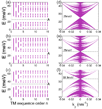
In Fig. 2 (a) and (b), we plot the trace maps for two kinds of graphene-based TM sequences with the change of , at the incident angle . We take nm in Fig. 2(a), and nm in Fig. 2(b). We find that the passing bands are split into more and more sub-bands as increases; when the band structures almost become the discontinuous bands. However, we note that the center positions of the Gap A in Figs. 2(a) and 2(b) are the same, and the positions of other gaps are shifted with the change of the lattice constant. Corresponding to Fig. 2(a) and 2(b), the electronic band structures for a TM sequence of have been shown in Fig. 2(d) and 2(e), respectively. It is seen that a new DP appears inside the Gap A and this new DP actually locates at
| (5) |
This condition is valid for periodic and aperiodic graphene superlattices LBrey2009 ; LGWang2010 ; XiChen2011 . Since in our cases, it is easily to obtain the energy for as follows:
| (6) |
This condition is different from the case of the Fibonacci sequence, which depends on the ration of numbers of layer A and B XiChen2011 . Actually, our formula (5) is valid for the condition of the new DP in the graphene-based Fibonacci sequence. Here we would like to emphasize that for the TM sequence, the location of the DP is independent of order ; while for the Fibonacci sequence it changes for different order . As an example for the TM sequence, in cases of Fig. 2(a,b,d,e), it is given by meV since .
Since the center of the Gap A in Fig. 2 is located at zero-, which is denoted by a dashed black line in Fig. 2(a) and 2(b), we may call it as the zero- gap. According to Eq.(6), the position of the zero- gap for the TM sequences is not shifted with the lattice constant itself, but is shifted with the change of the ratio of . As shown in Fig.2(c) and (f), the position of the zero- gap and the DP move to meV when .
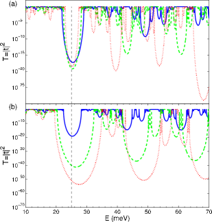
Fig.3 (a) shows the effect of the lattice constants on the electronic transmission spectrum. Based on Fig. 3(a), it is obvious that the zero- gap is insensitive to the lattice constants themselves. However, the positions of other gaps and passing bands with higher energy are highly dependent on the lattice parameters. From Fig. 3(b), one can also find that the position of zero- gap is weakly dependent on the incident angle , while other Bragg gaps change sensitively with .
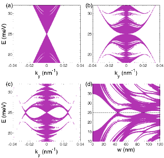
Furthermore, one has known that the multi-Dirac-points could appear in the GSLs with periodic potential structures LBrey2009 ; LGWang2010 . Here we point out that the extra Dirac points, located at , could also emerge in the GSL TM sequence as the lattice constant increases. See Figs. 4(a) and (b), the slope of the band edges near the DP gradually turns smaller as () increases from 20 nm to 40 nm. When () is larger than 40 nm, as that shown in Fig. 4 (c), the additional Dirac points appear at the same energy. From Figs. 4(a) to 4(c), we may also find the appearance of additional Dirac points associating with the variation of the zero- gap. In Fig. 4 (d), we show the energy band gaps as a function of the lattice constants in the case of . In the process of the appearance of the additional Dirac points, the zero- gap opens and closes oscillationally while the other gaps are shifted greatly.
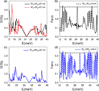
Finally, we calculate the total conductance SDatta1995 and the Fano factor JTwor2006 in GSL TM sequences, which are given by = and = where = and = with denoting the width of the graphene stripe in the direction. In Fig. 5, we present the total conductance and the Fano factor as a function of Fermi energy with different lattice constants. What we should notice is that the angular-averaged conductance ’s curve reaches its minimum at the DP and forms a linear cone around the DP, and at the DP’s location reaches the value of approximately XXGuo2011 ; JTwor2006 . From Fig. 5, we also find that the conductance and the Fano factor shift with the ratio of since the DP’s location relies on this ratio. Therefore, this indicates that the conductance of GSL TM sequence could be modulated by the ratio of the lattice constants. In addition, we should point out that, if one compares the passing bands of Fig. 2(a) in our case with those of Fig. 2(a) in Ref. XiChen2011 , one can easily find that the splitting behavior of bands in the TM sequence is very different from that in the Fibonacci case. Correspondingly, the electronic transport properties (the values of G and F) are different from those in the Fibonacci case. These distinct differences between the TM and Fibonacci sequences will be presented in our future work.
In summary, we have studied the electronic transport properties in the graphene-based Thue-Morse aperiodic sequence. It is shown that the extra-DPs can appear under some suitable conditions. The zero- gap associated with the DP is robust against the lattice constants and the incident angles, and the resultant controllable electron transport may facilitate the development of graphene-based electronics.
Acknowledgements.
This work is supported by NSFCs (Grant. No. 11104014 and No. 61078021), Research Fund for the Doctoral Program of Higher Education of China 20110003120007 and the National Basic Research Program of China (Grant No. 2012CB921602).References
- (1) K. S. Novoselov, A. K. Geim, S. V. Morozov, D. Jiang, Y. Zhang, S. V. Dubonos, I. V. Grigorieva, and A. A. Firsov, Science 306, 666 (2004).
- (2) Y. Zhang, Y. W. Tan, H. L. Stormer, and P. Kim, Nature (London) 438, 201 (2005).
- (3) A. B. Kuzmenko, E. van Heumen, F. Carbone, and D. van der Marel, Phys. Rev. Lett. 100, 117401 (2008).
- (4) F. Wang, Y. Zhang, C. Tian, C. Girit, A. Zettl, M. Crommie, and Y. R. Shen, Science 320, 206 (2008).
- (5) X. Chen and J.-W. Tao, Appl. Phys. Lett. 94, 262102 (2009).
- (6) A. H. Castro Neto, F. Guinea, N. M. R. Peres, K. S. Novoselov, and A. K. Geim, Rev. Mod. Phys. 81, 109 (2009).
- (7) Tianxing Ma, F. M. Hu, Z. B. Huang, and Hai-Qing Lin, Appl. Phys. Lett. 97, 112504 (2010); F. M. Hu, Tianxing Ma, Hai-Qing Lin, and J. E. Gubernatis, Phys. Rev. B 84, 075414 (2011).
- (8) N. M. R. Peres, Rev. Mod. Phys. 82, 2673 (2010).
- (9) S. A. Wolf, D. D. Awschalom, R. A. Buhrman, J. M. Daughton, S. von. Molnár, M. L. Roukes, A. Y. Chtchelkanova, and D. M. Treger, Science 294, 1488 (2001); K. Ando, ibid. 312, 1883 (2006).
- (10) R. Tsu, Superlattice to Nanoelectronics (Elsevier, Oxford, 2005).
- (11) J. C. Meyer, C. O. Girit, M. F. Crommie, and A. Zettl, Appl. Phys. Lett. 92, 123110 (2008).
- (12) S. Marchini, S. Günther, and J. Wintterlin, Phys. Rev. B 76, 075429 (2007).
- (13) A. L. Vazquez de Parga, F. Calleja, B. Borca, M. C. G. Passeggi, Jr., J. J. Hinarejos, F. Guinea, and R. Miranda, Phys. Rev. Lett. 100, 056807 (2008).
- (14) C.-X. Bai and X.-D. Zhang, Phys. Rev. B 76, 075430 (2007).
- (15) M. Barbier, F. M. Peeters, and P. Vasilopoulos, Phys. Rev. B 80, 205415 (2009).
- (16) L. Brey and H. A. Fertig, Phys. Rev. Lett. 103, 046809 (2009).
- (17) L.-G. Wang and S.-Y. Zhu, Phys. Rev. B 81, 205444 (2010); L.-G. Wang and X. Chen, J. Appl. Phys. 109, 033710 (2011).
- (18) Pei-Liang Zhao and Xi Chen, Appl. Phys. Lett. 99, 182108 (2011).
- (19) C. H. Park, L. Yang, Y. W. Son, M. L. Cohen, and S. G. Louie, Phys. Rev. Lett. 101, 126804 (2008).
- (20) X.-X. Guo, D. Liu, and Y.-X. Li, Appl. Phys. Lett. 98, 242101 (2011).
- (21) M. Queffélec, Substitution Dynamical Systems-Spectral Analysis, Lecture Notes in Mathematics Vol. 1294 (Springer, Berlin, 1987).
- (22) Z. Cheng, R. Savit, and R. Merlin, Phys. Rev. B 37, 4375 (1988).
- (23) F. Axel and J. Peyriere, J. Stat. Phys. 57, 1013 (1989).
- (24) J. M. Luck, Phys. Rev. B 39, 5834 (1989).
- (25) X. Y. Jiang, Y. G. Zhang, S. L. Feng, K. C. Huang, Y. Yi, and J. D. Joannopoulos, Appl. Phys. Lett. 86, 201110 (2005).
- (26) H. Noh, Jin-Kyu Yang, S. V. Boriskina, M. J. Rooks, G. S. Solomon, L. D. Negro, and H.Cao, Appl. Phys. Lett. 98, 201109 (2011).
- (27) Nian-hua Liu, Phys. Rev. B 55, 3543 (1997).
- (28) M. Kolář, M. K. Ali, and F. Nori, Phys. Rev. B 43, 1034 (1991).
- (29) F. Axel, J. P. Allouche, M. Kléman, M. Mendès-France, and J.Peyrière, J. Phys. (Paris) Colloq. 47, C3-181 (1986).
- (30) S. Datta, Electronic Transport in Mesoscopic Systems (Cambridge University Press, Cambridge, England, 1995).
- (31) J. Tworzydlo, B. Trauzettel, M. Titov, A. Rycerz, and C. W. J. Beenakker, Phys. Rev. Lett. 96, 246802 (2006).