Persistent electrical doping of Bi2Sr2CaCu2O8+x mesa structures
Abstract
Application of a significantly large bias voltage to small Bi2Sr2CaCu2O8+x mesa structures leads to persistent doping of the mesas. Here we employ this effect for analysis of the doping dependence of the electronic spectra of Bi-2212 single crystals by means of intrinsic tunneling spectroscopy. We are able to controllably and reversibly change the doping state of the same single crystal from underdoped to overdoped state, without changing its chemical composition. It is observed that such physical doping is affecting superconductivity in Bi-2212 similar to chemical doping by oxygen impurities: with overdoping the critical temperature and the superconducting gap decrease, with underdoping the -axis critical current rapidly decreases due to progressively more incoherent interlayer tunneling and the pseudogap rapidly increases, indicative for the presence of the critical doping point. We distinguish two main mechanisms of persistent electric doping: (i) even in voltage contribution, attributed to a charge transfer effect, and (ii) odd in voltage contribution, attributed to reordering of oxygen impurities.
pacs:
74.72.Gh, 74.62.Dh, 74.55.+v, 74.72.KfI Introduction
High temperature superconductivity (HTSC) in cuprates occurs as a result of doping of a parent antiferromagnetic Mott insulator and properties of cuprates change significantly with doping. Superconductivity in overdoped cuprates is fairly well described by the conventional BCS-type second-order phase transition TallonPhC ; SecondOrder ; MR . But properties of underdoped cuprates are abnormal due to the persistence of the normal state pseudogap, strong superconducting fluctuations, or possibly preformed pairing, Kaminski and magnetism Kerr_Shen at . There are indications that the transition from the normal to the abnormal behavior occurs abruptly at a critical doping point TallonPhC ; Doping ; Balakirev ; Kartsovnik ; LeBoeuf2011 . This may be a consequence of the quantum phase transition - a phase transition, which occurs at , in frustrated systems as a result of a competition of coexisting order parameters. The coexistence of superconductivity at with the pseudogap KrasnovPRL2000 ; Lee2007 ; Bernhard , charge and spin density order Kartsovnik ; LeBoeuf2011 ; Nernst2010 was indeed reported by several techniques. Clearly, detailed doping-dependent studies are needed both for understanding the puzzling nature of HTSC in cuprates and for the development of novel HTSC materials.
Usually, the mobile carrier concentration is controlled by chemical doping via chemical substitution, or in case of cuprates also by variation of the oxygen content via appropriate annealing and subsequent quenching to room temperature. This allows an accurate control of the chemical composition, but less so of the local arrangement of impurities and disorder, which is equally important for cuprates DisorderBi2201 . For example, it is well established that properties of the compound strongly depend not only on the average oxygen concentration but also crucially on the order/disorder of oxygen atoms in Cu-O-Cu chains Chains ; Raman . Therefore, analysis of the doping phase diagram of cuprates requires accurate control of both, the concentration and the microscopic structure of impurities.
The carrier concentration can be also varied via two physical doping processes, well established for semiconductors: photo-doping Kudinov ; Schuller ; PhotoScience2011 and through the electric-field effect Ahn ; Moeckly ; Sorkin ; Tulina ; KovalCurrentInj ; KovalMemres . In case of cuprates, physical doping may be persistent at low temperatures in a sense that it is relaxing very slowly after removing the light Kudinov ; Schuller or field Moeckly ; Tulina ; KovalCurrentInj ; KovalMemres . Recently, a persistent electric doping via strong current injection was discovered KovalCurrentInj ; KovalMemres . It is resembling a resistive switching phenomenon in memristor devices Memristor1 ; Memristor2 and is related to previous similar observations in point contact experiments on Bi2Sr2CaCu2O8+x (Bi-2212) Tulina . Such an electric doping is reversible, reproducible and easily controllable. It opens a possibility to analyze the doping dependence of HTSC on one sample without changing its chemical composition PhotoScience2011 . Despite that, there were very few direct spectroscopic studies of cuprates employing physical doping techniques.
Intrinsic Tunneling Spectroscopy (ITS) provides an unique opportunity to probe bulk electronic properties of HTSC SecondOrder . This technique utilizes weak interlayer (-axis) coupling in quasi two dimensional HTSC compounds, in which mobile charge carriers are confined in CuO2 planes separated by some blocking layer (e.g. SrO-2BiO-SrO in case of Bi-2212). This leads to a formation of atomic scale intrinsic tunnel junctions, and to an appearance of the intrinsic Josephson effect at Kleiner94 ; KrasnovPRL2000 ; Suzuki ; Katterwe2009 ; Superluminal .
In this work we employ the persistent electric doping for analysis of the doping dependence of electronic spectra of Bi-2212 single crystals by means of intrinsic tunneling spectroscopy SecondOrder ; Doping ; MR ; KrasnovPRL2000 ; KatterwePRL2008 . Controllable and reversible persistent physical doping is achieved by applying a -axis voltage of a few volts to small Bi-2212 mesa structures. Thus we are able to change the doping state of Bi-2212 single crystals without changing its chemical composition. A wide doping range from a moderately underdoped to strongly overdoped state could be reached. It is observed that the physical doping is affecting the intrinsic tunneling characteristics of Bi-2212 similar to chemical doping Doping . With overdoping the critical temperature and the superconducting gap decrease. With underdoping the pseudogap rapidly increases, indicative for the presence of the quantum critical doping point in the phase diagram, and the -axis critical current density rapidly decreases, indicating a progressively more incoherent interlayer tunneling. We distinguish two main mechanisms of persistent electric doping: (i) an even in voltage contribution, attributed to a charge transfer effect, and (ii) an odd in voltage contribution, attributed to reordering of oxygen impurities.
The paper is organized as follows. In Sec. II we make a brief overview of physical doping mechanisms of cuprates. Sec. III provides experimental details. In Sec. IV we present the main experimental results and in Sec. V we discuss possible mechanisms of persistent electric doping, followed by conclusions.
II Physical doping of cuprates
II.1 Photo-doping
Photo-doping allows a wide-range variation of doping in the same sample Kudinov ; Schuller ; PhotoScience2011 . The ordinary non-equilibrium photo-doping is quickly relaxing because of a very short life time (ps) of photoinduced charge carriers PhotoScience2011 . However, in underdoped and some other cuprates a different type of persistent photo-doping takes place Kudinov ; Schuller . It involves significant energies , which makes it metastable at low temperatures. Several mechanisms are contributing to the persistent photo-doping PhDopTheory , such as charge transfer, which changes the redox state of the impurity atom Kudinov , and ordering of oxygen impurities in the lattice Schuller . Photo-doping always leads to an increase of the doping level with respect to the initial state.
II.2 Electric field effects
Electric fields may both increase or decrease the number of mobile charge carriers, depending on the direction of the applied field Ahn . The ordinary electric field effect is not persistent and exists only during the time an electric field is applied. Since the electric field penetrates only to the Thomas-Fermi charge screening length, , just a thin surface layer can be modified Shapiro .
A persistent electrostatic field-effect due to net electric polarization or trapped charges can be realized at the interface between a superconductor and a ferroelectric SuperFerro or polar insulator ElStatic . This is also a surface phenomenon, but in case of layered cuprates, which represent stacks of metallic CuO planes sandwiched between polar-insulating layers Polariton , electrostatic charging of insulating layers may in principle lead to the bulk persistent electrostatic field-effect.
Another type of a persistent and bulk electric-field effect has been observed at large current densities Moeckly . Similar to photo-doping, it was attributed to a charge transfer Salluzzo2008 and reordering of oxygen impurities Sorkin . Significant oxygen mobility in intense electric fields also leads to a resistive switching phenomenon Tulina .
II.3 Resistive switching in complex oxides
The resistive switching phenomenon occurs in many complex oxides and is the basis for the development of resistive memory devices. Several mechanisms may be involved in the resistive switching phenomenon Memristor1 ; Memristor2 , including a change of the redox state of some of the elements, oxygen migration, and filament formation. Resistive switching has been observed on depleted surfaces of Bi-2212 cuprates Tulina and attributed to oxygen migration. Recently, it was demonstrated that the resistive switching-like phenomenon can be used for controllable and reversible doping of small Bi-2212 micro-structures over a wide doping range KovalCurrentInj ; KovalMemres .
III Experimental
Mesas were fabricated on top of freshly cleaved Bi-2212 single crystals by means of optical lithography, Ar ion milling and focused ion beam trimming. Four batches of crystals were used: pure near optimally doped (OP) Bi-2212, pure strongly underdoped (UD) Bi-2212, lead-substituted [Bi(Pb)-2212], and yttrium-doped [Bi(Y)-2212]. Mesas of different sizes from to and with a different number of junctions were studied. Details of the sample fabrication can be found in Ref. Submicron . All studied mesas exhibited a persistent doping effect upon application of a sufficiently large bias voltage.
The samples were placed in a flowing gas cryostat and measured in a three-probe configuration with a common top gold contact. The ground contacts for current and voltage were provided through other mesas on the same crystal. A Keithley K6221 current source and a FPGA-based arbitrary waveform generator and lock-in amplifier were used to bias and measure the samples. Biasing was done at pseudo-constant voltage, with an optional small superimposed ac voltage to simultaneously measure the high-bias differential resistance in addition to the dc resistance. Positive bias is defined as current going into the mesa through the common top contact, as sketched in Fig. 1 (a).
IV Results
From chemical (oxygen) doping studies it is known that doping/undoping of Bi-2212 is accompanied by a proportional decrease/increase of the -axis resistivity Doping . Therefore, we can control the doping state by tracing the mesa resistance.
IV.1 Dynamics of electric doping
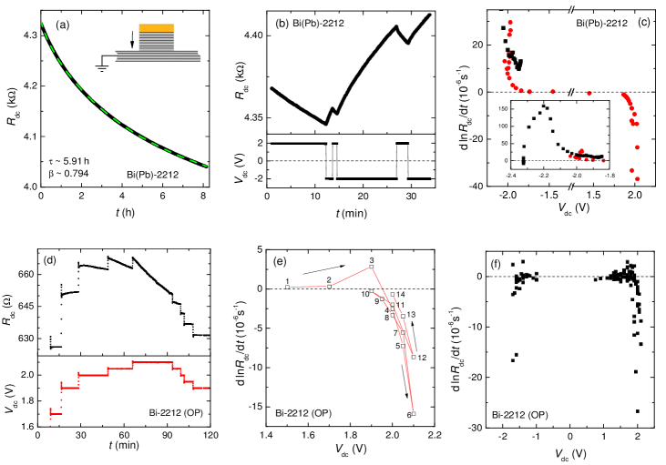
The basic features of the dynamics of the persistent electric doping are shown in Fig. 1. Panel (a) shows the time-evolution of the Bi(Pb)-2212 mesa resistance at a bias of at . It is seen that the mesa resistance is decreasing with time, indicating a gradual doping of the mesa. The doping rate decreases with time, following a stretched exponential decay, , shown by the dashed line in in Fig. 1 (a), which is also typical for persistent photo-doping Kudinov ; Schuller . The doping can be equally well performed at any temperature from 4 to 300 K, but the rate is increasing with . In most cases we perform doping at low in order to be able to immediately probe the superconducting characteristics. Upon reduction of the bias below the threshold voltage the state of the mesa remains stable even at room temperature on the time scale of several days.
The resistive change is reversed upon voltage reversal, as illustrated in Figs. 1 (b) and (c) for the same Bi(Pb)-2212 mesa. The resistance decreases for positive bias (electric field into the crystal) and increases for negative bias (electric field towards the top contact), which indicates that we can controllably and reversibly dope and undope the mesa. The doping rate and direction depend both on the sign and the absolute value of bias voltage.
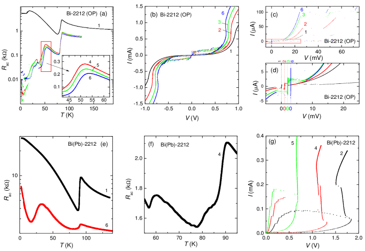
Figure 1 (c) summarizes the bias dependence of the doping rate for the Bi(Pb)-2212 mesa. Below the threshold voltages, , the mesa resistance is stable. Upon increasing the bias voltage, the resistance of the mesa starts to gradually change at a rate that increases drastically up to as shown in the inset of Fig. 1 (c). A further voltage increase reduces the rate and then reverses the resistance alteration rate (see the inset at ). The sign change of the alteration rate at high bias is in agreement with the observations by Koval et al. KovalCurrentInj . The behavior in this regime is, however, history dependent, as may be seen from Fig. 1 (c), and the final state depends on how long time the mesas was biased at every bias voltage. The doping process for the Bi(Pb)-2212 mesa, Fig. 1 (c), is predominantly odd in bias voltage, i.e., the direction of doping is changed when the sign of the bias voltage is changed.
Figures 1 (d) and (e) show a detailed view of the time and voltage dependence of doping for a near optimally doped pure Bi-2212 mesa. The top panel of (d) shows the time evolution of the resistance of an OP Bi-2212 mesa for different bias voltages, shown in the bottom panel. It is seen that the resistance is constant at , and starts to increase slowly at 1.9 V. However, at 2 V the resistance initially increases but then starts to decrease after a few minutes. This clearly shows that there are two counteracting processes: a positive rate mechanism that saturates quickly and a mechanism with negative rates that is dominating at longer times and at higher voltages. The second process also saturates with time, which is clear from Fig. 1 (a) and history dependent rates of Fig. 1 (e). At larger voltage, the resistance steadily decreases at a rate which is strongly bias dependent, as shown in Fig. 1 (f).
Figures 1 (e,f) show the bias dependence of doping and a history dependence upon sequential voltage sweeps (e). It is seen that for the OP Bi-2212 mesa the electric doping is predominantly even in voltage, i.e., the direction of doping does not depend on the sign of the bias voltage. However, certain asymmetry of the doping rate versus bias voltage characteristics in Figs. 2 (c) and (f) indicates the presence of sub-dominant even- and odd-in-voltage contributions for Bi(Pb)-2212 and OP Bi-2212 mesas, respectively.
IV.2 Doping dependence of ITS characteristics
Using the described method, the superconducting properties of the mesas have been altered to different intermediate doping states denoted by a successive number. The electric doping changes all mesa characteristics: the -axis resistivity, the critical temperature , the -axis critical current density , the superconducting energy gap, , the -axis pseudogap and the -axis resistivity in a manner very similar to chemical (oxygen) doping Doping .
Figure 2 shows temperature dependencies of low bias ac-resistances for the initial, high resistance state (HRS), and doped, lower resistance states (LRS), for (a) an OP Bi-2212 and (e,f) a Bi(Pb)-2212 mesa. The - characteristics of those mesas at different doping states are presented in panels (b-d) and (g), respectively.
From Fig. 2 (a) it is seen that the initial state was characterized by the strong thermal-activation-type increase of resistance with decreasing , typical for underdoped Bi-2212 Katterwe2009 . The general shape of the resistive transition was described in Ref. SecondOrder . At the resistance dropped to the top-contact resistance, which originates from the first deteriorated junction between the top CuO plane, shortly exposed to atmosphere after cleavage, and the second, un-deteriorated CuO plane SecondOrder . Initially this junction had a very low and a very small critical current, , as can be seen from the corresponding - in panel (d). After electric doping, the resistance in the normal state dropped almost three times and became less semiconducting. The main of the mesa changed only slightly, indicating that the doping was changing around the optimal doping level with the flat vs. doping dependence. However, the properties of the top junction changed drastically: the increased to , and the critical current increased ten-fold as shown in panel (d), even though it still remains times smaller than for the rest of the junctions in the mesa, as can be seen from panel (c). This indicates that the surface CuO plane was initially strongly underdoped and, therefore, responded much stronger to variation of doping, due to the steep vs. doping dependence at the underdoped side of the doping phase diagram of cuprates Doping . A similar trend was also observed in photo-doping Kudinov ; Schuller .
Another possible reason for the stronger response of the underdoped top junction is the larger -axis resistivity of underdoped intrinsic Josephson junctions Doping . Because of that the electric field is not uniformly distributed along the mesa but is larger in the high-resistive top junction. This together with the strong voltage dependence of the electric doping leads to a faster doping of the top junction and the doping may even go in the opposite direction with respect to the rest of the mesa.
The effect of non-uniform doping along the height of the mesa becomes more pronounced in higher mesas with a larger number of intrinsic Josephson junctions. This is seen from for the Bi(Pb)-2212 mesa from Fig. 2 (e), which contained a fairly large number of junctions . It is seen that after doping some junctions retained the initial , but some were very strongly overdoped to . Fig. 2 (f) shows at the intermediate doping state 4. Small drops represent critical temperatures of individual junctions in the mesa. Apparently there is a gradual distribution of along the height of the mesa.
Doping of Bi-2212 leads to a rapid increase of the -axis critical current density Doping . This is clearly seen from - curves for the Bi-2212 (OP) mesa shown in Figs. 2 (b-d). The increase of of the surface junction is shown in panel (d). One-by-one switching of the rest of the junctions into the resistive state at leads to the appearance of multiple-quasiparticle (QP) branch structures in the - curves. The corresponding critical current at the first QP branch is shown in panel (c). It also strongly increases with doping. The same effect doubles in the Bi(Pb)-2212 mesa, in Fig. 2 (g).
From Fig. 2 (b) it is seen that the - curves exhibit a kink at large bias, followed by an ohmic tunnel resistance. The kink represents the sum-gap singularity in superconducting tunnel junctions at per junction SecondOrder ; MR . This is the basis of the ITS technique, which allows analysis of the superconducting energy gap in the bulk of the Bi-2212 single crystal.
Accurate analysis of the electronic spectra with the ITS technique requires mesas with a small area and a small number of identical junctions. This is needed for avoiding possible artifacts, associated with self-heating, in-plane non-equipotentiality, and spread in junction parameters Heating_PRL2005 ; SecondOrder . This is particularly important for the analysis of the genuineshape of tunneling characteristics, which remains a controversial issue Comment2 . Even though the - characteristics in Figs. 2 (b) and (g) are distorted by self-heating, as evident from a back-bending at large bias, the general trend for a variation of the sum-gap kink with doping is clearly seen: The superconducting gap decreases and the sum-gap kink becomes sharper with (over-)doping. This qualitative conclusion is not affected by self-heating because the dissipation power at the kink decreases with decreasing resistance and becomes smaller with subsequent doping. Thus, with over-doping the superconducting sum-gap singularity becomes sharper and moves to lower voltages despite the progressive reduction of self-heating. This clearly reveals the doping-variation of the genuine -axis tunneling characteristics Comment2 . A similar tendency was observed by other techniques, including the angular resolved photoemission spectroscopy ARPES_doping , scanning tunneling spectroscopy STS_inhomo , and tunneling spectroscopy on point contacts Zasad_doping , as well as in previous ITS studies involving chemical (oxygen) doping Doping ; KatterwePRL2008 ; SecondOrder .
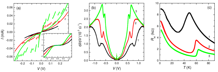
Figure 3 shows the electric doping of an initially strongly underdoped Bi-2212 mesa. A five-fold increase in critical current in the - characteristics (a), and an increase of of about 15 K (c) can be seen. The tunneling conductance curves are shown in panel (b). It is seen that the sum-gap peak shifts to slightly lower voltages and becomes sharper with doping. The hump voltage, attributed to the -axis pseudogap SecondOrder , rapidly decreases with increasing conductance, pointing towards an abrupt opening of the pseudogap at the critical doping point, consistent with chemical doping studies Doping ; Balakirev ; Bernhard .
Note that in all studied cases the electric doping has lead to a significant increase of the critical current, while the superconducting gap was decreasing. The anticorrelation between and in underdoped Bi-2212 has been reported before Doping and was attributed to progressively more incoherent -axis transport in combination with the -wave symmetry of the superconducting order parameter.
IV.3 Short-pulse doping
So far we were discussing a gradual electric doping of Bi-2212 mesas at the time scale of an hour, as shown in Fig. 1. Such a long time doping allows a very strong variation of the doping state, but often leads to inhomogeneous doping within the mesa height, as shown in Fig. 2. Koval et.al. KovalMemres demonstrated that a short-pulse doping strategy leads to highly reversible and reproducible doping, similar to resistive switching in point contacts Tulina . This is probably related to the lack of significant electromigration during the short pulse, which may eventually lead to an irreversible destruction of the crystal structure Moeckly .
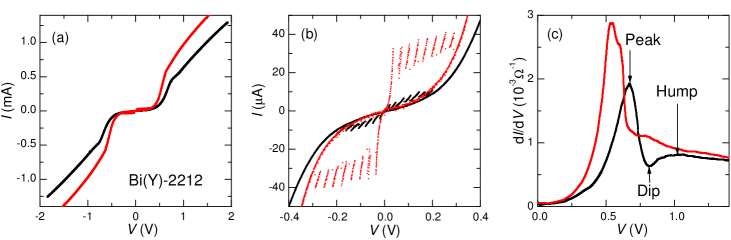
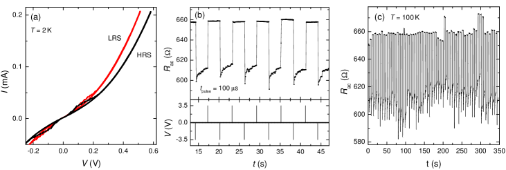
Figure 4 represents the ITS characteristics at for a small Bi(Y)-2212 mesa with a small amount of junctions and small self-heating Heating_PRL2005 . In the initial high-resistive state the mesa is slightly underdoped with . The mesa was switched to a low-resistive state by a short voltage pulse of about a milliseconds width. The periodicity of QP branches in Fig. 4 (b) demonstrates that after switching into the LRS the mesa remains highly uniform. From comparison of - curves in panels (a) and (b) it is seen that the decrease of resistance by is accompanied by an almost four-fold increase of . The increased to being an indication that the mesa became near optimally doped.
Fig. 4 (c) represents the tunneling conductance in the high-resistive (underdoped) and the low-resistive (optimally doped) states. The following main changes in ITS spectra are seen: the superconducting sum-gap peak voltage decreased in the doped low resistive state and the shapes of spectra are changed. The relative sum-gap peak height is increased by about 50% in the low-resistive state. The high-resistive state exhibits a peak-dip-hump structure, which is less obvious in the low-resistive state. All this is similar to the slow-doping case, Figs. 2 and 3, and consistent with the change of doping from the slightly underdoped to near optimally-doped state Doping , in accordance with other spectroscopic studies involving chemical (oxygen) doping ARPES_doping ; STS_inhomo ; Zasad_doping .
As already discussed above, the increase of sharpness of the sum-gap kink in the - curve and the peak in the curve in the low-resistive state, reported in Figs. 2 and 4, and the change of the shape of the peak-dip-hump feature in Fig. 4 (c) can not be attributed to self-heating, because the actual power dissipation at the peak is decreasing in the low-resistive state. For example, the corresponding powers at the peaks in Fig. 4 (c) are and 0.17 mW, respectively. This observation supports the conclusion of Ref. Comment2 that the appearance and the shape of the peak-dip-hump structure in the ITS characteristics of small mesas is determined primarily by the doping level.
A detailed analysis of short pulsed resistive switching has been performed on strongly underdoped Bi-2212 mesas. For negative pulses with length and compliance voltages up to there was no resistive switching. At , a reduction of the quasiparticle resistance to 99.3% is observed (LRS). Nine subsequent pulses reduce the resistance further to 98.4%. A single positive pulse switches the resistance back to the initial HRS, while more positive pulses do not result in additional changes. A single negative pulse with a higher compliance voltage of instead reduces the resistance of the LRS to about 93.4% of the HRS, and the corresponding positive pulses switches it back. Pulses with lower compliance voltage lead to a partial switching but additional pulses with the same compliance do not lead to a significant change. Fig. 5 (a) shows - curves of another UD Bi-2212 mesa at in the HRS and the LRS obtained with a pulse of width. The general difference between -s after the pulsed doping in Figs. 4 (a) and 5 (a) is the same as for the slow doping in Figs. 2 (a) and 3 (a).
Fig. 5 (b) demonstrates a reproducible resistive switching between HRS and LRS at elevated for another UD Bi-2212 mesa. The switching was performed using a similar positive and negative pulse sequence with , a pulse width of and an interval between pulses of 3 s, shown in the bottom panel of Fig. 5 (b). Panels (b) and (c) show the corresponding time sequence of the measured zero-bias resistance of the mesa. It is seen that negative voltage pulses lead to switching into the LRS while a subsequent positive pulse switches the mesa back into the HRS. The corresponding resistance change rates are of the order of , which are somewhat higher than for the slow doping shown in Fig. 1 (d), but not inconsistent with that data, taking into account that the compliance voltage is also significantly higher. It is seen that the HRS is stable and shows no visible relaxation at , while the LRS is initially relaxing with the characteristic time and then saturates before reaching the HRS, as shown in panel (b). At , the behavior is similar with a time constant of .
V Discussion: mechanisms of persistent electric doping
In Sec. II we briefly reviewed known mechanisms of persistent physical doping of cuprates. It is likely that some of them are playing a role in persistent electric doping, studied here. Indeed, the phenomenon is clearly related to the persistent electric-field effect Moeckly , observed in , which in turn is clearly related to persistent photo-doping observed for various cuprates Kudinov ; Schuller .
To identify possible mechanisms, we first summarize characteristic features of the persistent electric doping:
i) Observed different voltage dependencies (odd and even) indicate that several distinct mechanisms are involved.
ii) The doping rate shows a threshold-like behavior as a function of bias voltage (see Fig. 1). The threshold voltage depends on in a thermal-activation manner, i.e. decreases with increasing . Remarkably, the threshold voltage is weakly dependent on the number of junctions in the mesa, consistent with previous reports KovalCurrentInj ; KovalMemres , and is comparable to that for a single point contact Tulina . This suggests that the phenomenon is connected to some characteristic energy , rather than directly to the electric field. Indeed, for a given voltage, the latter should scale inversely proportional to the number of junctions in the mesa, i.e., would not be universal for different mesas (that is why we hesitate to refer to the phenomenon as a persistent electric field effect, and rather call it persistent electric doping).
iii) However, the role of the electric field should not be underestimated. Indeed, the displacement field is given by , where is the dielectric constant and is the thickness of the insulating barrier between CuO bi-layers. The ratio was estimated from an analysis of Fiske (geometrical resonance) step voltages Superluminal . Therefore, the displacement field in intrinsic junctions is
| (1) |
For and , which corresponds to the case of Fig. 4, one would get a very large value , which is certainly capable of seriously polarizing and displacing ions in complex oxides Moeckly ; Tulina ; Memristor1 .
iv) The phenomenon is not associated with a net change of the oxygen content, which may only decrease within the cryostat. To the contrary, mesas can be repeatedly and reversibly doped and undoped, as shown in Figs. 1 (b) and 5 (b).
V.1 Charge transfer and electrostatic charge trapping
If an injected electron has a high enough energy, it may join one of the ions, leading to a change of the redox state and the effective doping. It was suggested that such a “charge transfer” mechanism is involved both in photo-doping of cuprates Kudinov and in the resistive switching phenomenon in other complex oxides Memristor1 .
Alternatively, the electron may be trapped (localized) in dielectric parts, leading to electrostatic charging of the sample. The Bi-2212 compound has a layered structure with metallic CuO planes sandwiched between polar insulator BiO layers Polariton . In this case the electrostatic charging will take place in BiO layers, which may affect the doping state of the neighboring CuO planes via the electrostatic field-effect. The electrostatic charging of means by current injection takes place uniformly within the whole structure. Therefore, unlike the conventional electric field effect Ahn and the electrostatic field effect at the interface between a superconductor and a ferroelectric material SuperFerro ; ElStatic , the current injection may lead to a persistent bulk electrostatic field-effect doping of Bi-2212. Koval et. al. KovalCurrentInj emphasized the similarity of the phenomenon with the floating-gate effect utilized in Flash memory devices.
Both types of charging effects have common similarities:
i) The charge transfer requires a certain energy (eV for ), rather than electric field.
ii) The sign of the current and the direction of the electric field does not matter. Therefore, such doping should be even with respect to the voltage sign, consistent with the observations in Ref. KovalCurrentInj .
Therefore, we attribute even in voltage persistent electric doping to charge transfer and/or charge trapping mechanisms.
V.2 Oxygen reorientation and reordering
It is well established that the doping state of cuprates depends not only on the amount of off-stoichiometric oxygen, but also on the relative orientation of the oxygen bonds Chains . Therefore, the doping state can be changed by oxygen reordering. Since the required energy is large , compared to thermal energies, oxygen reordering is a slow process and does not take place spontaneously at low enough . Oxygen reordering is considered as one of the main mechanisms of the persistent photo Schuller and electric field Moeckly doping.
In the case of persistent electric-field doping, the oxygen reordering is steered by the polarization. Therefore, the direction of doping should depend on the direction of the electric field, i.e., should be odd with respect to the bias voltage. We clearly see such a contribution in our experiment, see Fig. 1 (b). Note that the odd-in-voltage contribution was reported in the point-contact case Tulina , but not reported in previous related works made on zig-zag type Bi-2212 microstructures KovalCurrentInj ; KovalMemres . The geometry of the latter samples is symmetric with respect to the electric field direction (changing the sign of the electric field is equivalent to flipping their sample up-side down). This is not the case in point contacts and mesa structures, studied here, for which the fields down (into the crystal) and up (into the top electrode) are not equivalent. Therefore, the difference may partly be due to the difference in sample geometry, or to the observed sample-dependence of the relative strength of odd and even in voltage doping contributions, as shown in Figs. 1 (d) and (e).
Thus, we attribute the odd in voltage persistent electric doping mechanism to field-induced oxygen reorientation/reordering.
V.3 Irreversible processes: electromigration, filament and arc formation
An increase of the bias voltage above leads to a gradual increase of the current and irreversible change of the mesa properties. A similar phenomenon was observed in thin films and attributed to electromigration and field-induced diffusion of oxygen, which is even in bias voltage. The increase of conductance is probably due to a dielectric breakthrough in the insulating BiO layers, which leads to a pin-hole and filament formation. Thus, we attribute the slow and irreversible drift of the mesa characteristics at large bias voltages to electromigration in the mesas. This destructive process is, however, distinctly different from the reversible and reproducible electric doping effect, reported above.
After deterioration by electromigration, the mesa characteristics become similar to resistive switching characteristics for point contacts on top of oxygen-depleted, Bi-2212 surfaces Tulina . At even higher bias the resistance becomes very high (infinite). But an inspection in a microscope shows that the mesa itself remains intact. There is no physical evaporation of material or a crater at the place of the mesa, as in the case of a violent electric discharge. Instead there are clear indications of an arc formation at one of the sharp corners of the mesa, which probably leads to delamination of the structure and mechanical disattachment of the mesa from the base crystal.
V.4 Mechanisms of energy accumulation
The most puzzling property of the reported persistent electric doping is that the required bias voltage is weakly dependent on the number of junctions in the mesa KovalCurrentInj ; KovalMemres . This is clearly seen from the presented data, for which the threshold voltage is always for in Fig. 4, in Fig. 1 (f) and in Fig. 1 (d), which is also similar to that for a single point-contact V Tulina . It is, therefore, clear that electric doping requires a certain electron energy, rather than electric field. However, for stacked tunnel junctions, the energy acquired by the injected electron in every tunneling event is proportional to the voltage drop across the junction, , and is significantly smaller than the threshold energy. The main question is, therefore, how the electrons accumulate a sufficiently large energy, required for doping.
In Ref. KovalMemres it was suggested that an electron can accumulate energy upon sequential tunneling through several junctions without relaxation. However, in this case only electrons in the last junction will have enough energy. This would result in a strongly inhomogeneous doping in different junctions. Moreover, the probability of sequential tunneling without relaxation is small, because of the small ratio of relaxation time () Cascade to the tunnel time, , . The probability of sequential tunneling through junctions is decreasing rapidly with increasing . This should lead to a dramatic increase of the doping time with increasing . Indeed, suppose that it takes for junctions at to dope the mesa. This will involve tunneling events in each junction ( is the electron charge). Since the probability of sequential tunneling through junctions is decreasing quadratically, it would require tunneling events per junction, which will take . However, such a dramatic increase of the doping time with increasing mesa height is inconsistent with experiments.
For the sequential tunneling scenario to be relevant, the ratio should rapidly drop with increasing electron energy and become of the order of unity at . This may be caused by resonant tunneling, which increases the tunneling rate of quasiparticles with a certain energy, and/or by a drastic slowing down of the high energy quasiparticle relaxation, which may be caused by a rapid decrease of the Eliashberg’s electron-boson spectral function and a gap in the corresponding bosonic density of states at high energies Cascade . Such a scenario is interesting to investigate because it may give an information about the bosonic spectrum, involved in Cooper pairing, and thus provide a clue about the electron-boson coupling mechanism, responsible for high- superconductivity in cuprates Cascade .
We also want to propose an alternative mechanism for the energy accumulation of electrons: the formation of electric-field domains in the natural atomic superlattice formed by the mesa. Electric field domains are well studied in semiconducting superlattices Superlattice . They appear in weakly coupled superlattices close to the resonant tunneling condition. The corresponding non-linearity leads to an instability and a multiple-valued current-voltage characteristics. As a result, the electric field distribution in the superlattice becomes nonuniform and is concentrated in one or several junctions.
A possibility of a formation of electric field domains in Bi-2212 mesas is not just a hypothesis. In fact, the multiple-branch - of Bi-2212 mesas due to one-by-one switching of intrinsic junctions from the superconducting to the resistive state, shown in Fig. 4 (b), is due to a formation of electric field domains in individual tunnel junctions. The formation of electric field domains in Bi-2212 mesas at high bias would explain many of the features of the studied persistent electric doping. In this case electrons in the domain may gain an energy close to eV without sequential tunneling through the whole mesa. Furthermore, since domains are typically dynamic and propagate through the whole superlattice Superlattice , this would also explain the uniformity of doping in the whole mesa, and not just in the outermost junction.
VI Conclusions
We have studied the effect of persistent electric doping on intrinsic tunneling characteristics of small Bi-2212 mesa structures. It was shown that the application of a sufficiently large voltage to the mesas leads to a controllable and reversible physical doping of the mesas, without a modification of their chemical composition. This allows the analysis of bulk electronic spectra in Bi-2212 in a wide doping range on one and the same mesa. This physical doping has the same effect as chemical (oxygen) doping on the intrinsic tunneling characteristics of Bi-2212: the -axis resistivity decreases, the critical current increases and the energy gap is decreasing together with with over-doping. The anticorrelation between and indicates that the -axis transport becomes progressively more incoherent at the underdoped side of the phase diagram. An analysis of the doping variation of the intrinsic tunneling characteristics of the same mesa provides a clue about its genuine shape: with subsequent doping, the sum-gap peak in the tunneling conductance becomes sharper and the pseudogap hump rapidly decreases with doping, suggesting the presence of a critical doping point, in agreement with previous chemical doping studies Doping .
By analyzing the bias- and time dependence we could identify different mechanisms involved in the persistent electric doping: i) The even-in-voltage process via charge transfer and/or charge trapping. ii) The odd-in-voltage process via oxygen reordering. Those are distinct from the irreversible electromigration and oxygen electrodiffusion, observed at higher bias.
We confirm the previous report KovalMemres that the threshold voltage for the electric doping is weakly dependent of the number of junctions in the mesas and is similar to that for a single surface point contact Tulina . This indicates that it is the energy of injected electrons, rather than electric field, that determines the phenomenon. We suggest that the required energy accumulation by tunnel electrons may be due to a formation of electric field domains in the natural atomic superlattice formed in the Bi-2212 single crystal.
Acknowledgments We are grateful to the Swedish Research Council and the SU-Core Facility in Nanotechnology for financial and technical support.
References
- (1) J. L. Tallon, and J. W. Loram, Physica C 349, 53 (2001).
- (2) V. M. Krasnov, Phys. Rev. B 79, 214510 (2009).
- (3) V. M. Krasnov, H. Motzkau, T. Golod, A. Rydh, S. O. Katterwe, and A. B. Kulakov, Phys. Rev. B 84, 054516 (2011).
- (4) T. Kondo, Y. Hamaya, A. D. Palczewski, T. Takeuchi, J. S. Wen, Z. J. Xu, G. Gu, J. Schmalian, and A. Kaminski, Nature Phys. 7, 21 (2011).
- (5) R.-H. He, M. Hashimoto, H. Karapetyan, J. D. Koralek, J. P. Hinton, J. P. Testaud, V. Nathan, Y. Yoshida, H. Yao, K. Tanaka, W. Meevasana, R. G. Moore, D. H. Lu, S.-K. Mo, M. Ishikado, H. Eisaki, Z. Hussain, T. P. Devereaux, S. A. Kivelson, J. Orenstein, A. Kapitulnik, and Z. X. Shen, Science 331, 1579 (2011).
- (6) V. M. Krasnov, Phys. Rev. B 65, 140504(R) (2002).
- (7) F. F. Balakirev, J. B. Betts, A. Migliori, I. Tsukada, Y. Ando, and G. S. Boebinger, Phys. Rev. Lett. 102, 017004 (2009).
- (8) T. Helm, M. V. Kartsovnik, M. Bartkowiak, N. Bittner, M. Lambacher, A. Erb, J. Wosnitza and R. Gross Phys. Rev. Lett. 103, 157002 (2009).
- (9) D. LeBoeuf, N. Doiron-Leyraud, B. Vignolle, M. Sutherland, B. J. Ramshaw, J. Levallois, R. Daou, F. Laliberte, O. Cyr-Choiniere, J. Chang, Y. J. Jo, L. Balicas, R. Liang, D. A. Bonn, W. N. Hardy, C. Proust, and L. Taillefer Phys. Rev. B 83, 054506 (2011).
- (10) V. M. Krasnov, A. Yurgens, D. Winkler, P. Delsing and T.Claeson, Phys. Rev. Lett. 84, 5860 (2000).
- (11) W. S. Lee, I. M. Vishik, K. Tanaka, D. H. Lu, T. Sasagawa, N. Nagaosa, T. P. Devereaux, Z. Hussain and Z. X. Shen, Nature 450, 81 (2007).
- (12) L. Yu, D. Munzar, A. V. Boris, P. Yordanov, J. Chaloupka, Th. Wolf, C. T. Lin, B. Keimer and Ch. Bernhard, Phys. Rev. Lett. 100, 177004 (2008).
- (13) R. Daou, J. Chang, D. LeBoeuf, O. Cyr-Choiniere, F. Laliberte, N. Doiron-Leyraud, B. J. Ramshaw, R. Liang, D. A. Bonn, W. N. Hardy, and L. Taillefer, Nature 463, 519 (2010).
- (14) K. Fujita, T. Noda, K. M. Kojima, H. Eisaki, and S. Uchida, Phys. Rev. Lett. 95, 097006 (2005).
- (15) N. Chandrasekhar, O. T. Valls, and A. M. Goldman, Phys. Rev. B 49, 6220 (1994).
- (16) M. Käll, M. Osada, M. Kakihana, L. Börjesson, T. Frello, J. Madsen, N. H. Andersen, R. Liang, P. Dosanjh, and W. N. Hardy, Phys. Rev. B 57, 14072(R) (1998).
- (17) V. I. Kudinov, I. L. Chaplygin, A. I. Kirilyuk, N. M. Kreines, R. Laiho, E. Lähderanta, and C. Ayache, Phys. Rev. B 47, 9017 (1993).
- (18) A. Gilabert and A. Hoffmann and A. G. Medici and I. K. Schuller, J. Supercond. Novel Magn. 13, 1 (2000).
- (19) D. Fausti, R. I. Tobey, N. Dean, S. Kaiser, A. Dienst, M. C. Hoffmann, S. Pyon, T. Takayama, H. Takagi, and A. Cavalleri, Science 331, 189 (2011).
- (20) C. H. Ahn, A. Bhattacharya, M. Di Ventra, J. N. Eckstein, C. D. Frisbie, M. E. Gershenson, A. M. Goldman, I. H. Inoue, J. Mannhart, A. J. Millis, A. F. Morpurgo, D. Natelson, and J.-M. Triscone, Rev. Mod. Phys. 78, 1185 (2006).
- (21) B. H. Moeckly, D. K. Lathrop, and R. A. Buhrman, Phys. Rev. B 47, 400 (1993); S. H. Huerth, H. D. Hallen and B. Moeckly, Phys. Rev. B 67, 180506(R) (2003).
- (22) P. Konsin, and B. Sorkin, Phys. Rev. B 58, 5795 (1998).
- (23) N. A. Tulina, G. A. Emelchenco, and A. B. Kulakov, Physics Lett. A 204, 74 (1995); N. A. Tulina, A. M. Ionov, and A. N. Chaika, Physica C 366, 23 (2001); A. Plecenik, M. Grajcar, P. Seidel, S. Takacs, A. Matthes, M. Zuzcak, and S. Benacka, Physica C 301, 234 (1998).
- (24) Y. Koval, X. Jin, C. Bergmann, Y. Simsek, L. Özyüzer, P. Müller, H. Wang, G. Behr, and B. Büchner, Appl. Phys. Lett. 96, 082507 (2010).
- (25) Y. Koval, F. Chowdhury, X. Jin, Y. Simsek, F. Lichtenberg, R. Pentcheva, P. Müller, Phys. Status Solidi A 208, 284 (2011).
- (26) R. Waser, and M. Aono, Nature Materials 6, 833 (2007); R. Waser, R. Dittmann, M. Salinga, and M. Wuttig, Sol. St. Electr. 54, 830 (2010).
- (27) J. J. Yang, M. D. Pickett, X. Li, D. A.A. Ohlberg, D. R. Stewart, and R. S. Williams, Nature Nanotechn. 3, 429 (2008).
- (28) R. Kleiner, P. Müller, Phys. Rev. B 49, 1327 (1994).
- (29) K. Anagawa, Y. Yamada, T. Watanabe, and M. Suzuki, Phys. Rev. B 67, 214513 (2003).
- (30) S. O. Katterwe and V. M. Krasnov, Phys. Rev. B 80, 020502(R) (2009).
- (31) S. O. Katterwe, A. Rydh, H. Motzkau, A. B. Kulakov, and V. M. Krasnov, Phys. Rev. B 82, 024517 (2010).
- (32) S. O. Katterwe, A Rydh, and V. M Krasnov Phys. Rev. Lett. 101, 087003 (2008).
- (33) N. Kristoffel, and P. Rubin, Physica C 418, 49 (2005).
- (34) B. Y. Shapiro, Sol. St. Commun. 56, 149 (1985).
- (35) R. Aidam, D. Fuchs, and R. Schneider, Physica C 328, 21 (1999).
- (36) A. Walkenhorst, C. Doughty, X. X. Xi, Q. Li, C. J. Lobb, S. N. Mao, and T. Venkatesan, Phys. Rev. Lett. 69, 2709 (1992); X. X. Xi, J. Supercond. 7, 137 (1994).
- (37) S. O. Katterwe, H. Motzkau, A. Rydh, and V. M. Krasnov, Phys. Rev. B 83, 100510(R) (2011).
- (38) M. Salluzzo, G. Ghiringhelli, J. C. Cezar, N. B. Brookes, G. M. DeLuca, F. Fracassi, and R. Vaglio, Phys. Rev. Lett. 100, 056810 (2008).
- (39) V. M. Krasnov, T. Bauch, and P. Delsing, Phys. Rev. B 72, 012512 (2005).
- (40) V. M. Krasnov, M. Sandberg, and I. Zogaj, Phys. Rev. Lett. 94, 077003 (2005).
- (41) V. M. Krasnov, Phys. Rev. B 84, 136501 (2011).
- (42) H. Ding, J. R. Engelbrecht, Z. Wang, J. C. Campuzano, S.-C. Wang, H.-B. Yang, R. Rogan, T. Takahashi, K. Kadowaki, and D. G. Hinks, Phys. Rev. Lett. 87, 227001 (2001).
- (43) K. M. Lang, V. Madhavan, J. E. Hoffman, E. W. Hudson, H. Eisaki, S. Uchida, and J. C. Davis, Nature 415, 412 (2002).
- (44) L. Ozyuzer, J. F. Zasadzinski, K. E. Gray, C. Kendziora, and N. Miyakawa, Europhys. Lett. 58, 589 (2002).
- (45) V. M. Krasnov, Phys. Rev. Lett. 97, 257003 (2006); ibid., 103, 227002 (2009).
- (46) L. L. Bonilla, and H. T. Grahn, Rep. Prog. Phys. 68, 577 (2005).