Towards precise measurement of oscillatory domain wall by ferromagnetic Josephson junction
Abstract
We theoretically propose a principle for precise measurement of oscillatory domain wall (DW) by a ferromagnetic Josephson junction, which is composed of a ferromagnetic wire with DW and two superconducting electrodes. The current-voltage curve exhibits stepwise structures, only when DW oscillates in the ferromagnetic wire. The voltage step appears at with the fundamental constant , integer number , and the DW frequency . Since can be determined in the order of 10-9 accuracy, the oscillatory DW will be measured more precisely than present status by conventional method.
pacs:
74.50.+r, 76.50.+gNano-scale magnetic materials for spintronics devices are extensively studied due to many advantages such as enhanced operation speed, low power consumption, and high integration of memory cell.zutic ; maekawa Non-volatile memory using a magnetic domain wall (DW) is one example of such devices,allwood ; parkin and many studies are devoted to control DW.yamanouchi ; yamaguchi ; saitoh ; hayashi ; boone ; thiaville ; he07 ; bisig ; ieda Among those studies, the oscillatory DW is experimentally observedsaitoh ; hayashi ; boone and is examined toward applications, e.g. high sensitive magnetic sensor, nano-scale telecommunication, rf-assisted writing of magnetic bit, and microwave generator.kiselev ; thirion ; ono08 ; wang10 Once such devices are realized in a microscopic circuit, one needs to measure the DW frequency more precisely.
One example of precise measurement is the Josephson effect.josephson Under irradiation of microwave to the Josephson junction, the current-voltage (-) curve shows step structures at with microwave frequency , integer , and the ratio of the Plank constant and the elementary charge . This structure called Shapiro stepshapiro is adopted to the voltage standard around the world,hamilton ; kohlmann since the voltage can be determined in the order of 10-9 accuracy by the precise values of the frequency and the fundamental constants.hamilton ; kohlmann
On the other hand, many authors studied the Josephson effect in a hybrid structure of superconductor and ferromagnet.ryazanov_01 ; kontos ; sellier03 ; robinson ; robinson2 ; frolov In this ferromagnetic Josephson junction (FJJ), two superconducting electrodes are separated by a thin ferromagnetic layer, whose thickness is controlled in the order of nano meter.ryazanov_01 ; kontos ; sellier03 ; robinson ; robinson2 ; frolov If DW is put into the ferromagnetic layer of FJJ, it might be possible to measure the oscillatory DW more precisely by using the Josephson effect.

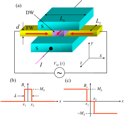
In this letter, by using FJJ, we theoretically propose a principle to measure the oscillatory DW more precisely than the present accuracy. As depicted in Fig.1(a), we use FJJ composed of a ferromagnetic Py wire with DW and two superconducting Nb electrodes. The interface is parallel to the -plane with width and depth . A dc bias current is applied to the -direction between the electrodes separated by height . We suppose the magnetic flux densities due to DW as shown in Figs. 1 (b) and (c), where is the saturation magnetization and . In such a magnetic flux density, a gauge invariant phase difference satisfies the differential equation,barone , where and is the unit vector perpendicular to the -plane. The solution is given by,
| (1) | |||||
| (2) | |||||
| (3) |
where and are both ends of DW. Below, the DW thickness is assumed to be constant.
The DW oscillation is driven by the external ac voltage parallel to the -direction with a certain frequency. Here, we assume that the width of DW is much smaller than , and DW harmonically oscillates within the junction. Then, the position of is expressed to be , where and are the oscillation amplitude and frequency of DW, respectively (see Figs. 1 (b) and (c)).
From Eqs. (1), (2), and (3), the Josephson current is given by
| (4) | |||||
where and for = , . The Josephson critical current and its density are denoted by and , respectively. The position and the width of DW are normalized as, and .
We examine the - curve in FJJ by the resistively shunted junction (RSJ) model,
| (5) |
with the resistance of junction and the flux quantum =.

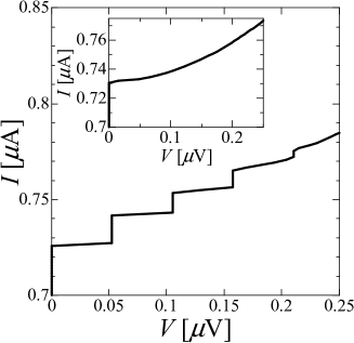
We numerically solve Eq. (5) and calculate the - curve by using the relation, , where denotes a time average. Figure 2 shows the - curve for the following parameters; =160 MHz, nm, =5 nm, =1 A, =0.75 T, and =1 .saitoh ; robinson ; robinson2 ; ando ; note1 We find the stepwise structure similar to the Shapiro step.shapiro This structure, on the other hand, disappears without the DW oscillation (see the inset of Fig. 2). It is noted that ferromagnetism and roughness of interface suppress the proximity effect in FJJ and then leads to the suppression of .ryazanov_01 ; kontos ; sellier03 ; frolov ; robinson ; robinson2 The obtained values in Fig. 2 are experimentally observable, i.e., in order of micro-ampere and micro-volt. In view of the measurement, the fabrication of flat interface and the choice of material is important.
To clarify the origin of the stepwise structure, we analytically examine the relation between the dc voltage and in the I-V curve. For this purpose, it is useful to note that Eq. (4) is written as,
where is the first kind Bessel function. To obtain Eq. (LABEL:ij-2), we suppose with a constant . The time-dependent term is due to the applied bias voltage. The DW oscillation modulates the phase variable such as with an amplitude . The stepwise structure can be associated with the dc component of , which is given by taking the time average of Eq. (LABEL:ij-2) and becomes finite for =. Therefore, the stepwise structures appear at the following voltages,
| (7) |
with integer . It is worth to note that Eq. (7) relates to only by the fundamental constant and . Therefore, we can precisely determine the frequency of DW oscillation by the - curve. Those fundamental constants are known as, =1.602 176 487(40) 10-19C and =1.054 571 628(53) 10-34Js with accuracy in order of .rmp80 On the other hand, is precisely determined by the conventional Josephson junction in the order of accuracy.hamilton ; kohlmann Hence, the measurement on can determine the DW frequency precisely. Accuracy of conventional measurement on the DW oscillation is limited in order of about , since those methods depend on material parameters such as anisotropic field, saturation magnetization and so on.saitoh ; boone Therefore, our method will be more precise than the present accuracy by conventional one.
So far, we have discussed the - curve in the FJJ composed of the ferromagnetic Py wire and superconducting Nb electrodes. If is larger than that of the Nb-based FJJ, one can expect a larger step height in the - curve, since each step heights are proportional to as shown in Eq. (LABEL:ij-2). Since increases with the superconducting gap and/or the transmittance of junction, NbN, NbTiN and high cuprates, which have larger gap compared with Nb, are possible candidates for superconducting electrodes.yang ; keizer For instance, typical of the NbTiN-based FJJ is about A/m2, which is hundred times larger than that of the Nb-based FJJ.note1 ; keizer
We theoretically propose a principle for precise measurement of oscillatory domain wall (DW) by a ferromagnetic Josephson junction (FJJ), which is composed of a ferromagnetic wire (FW) with DW and two superconducting electrodes. The current-voltage curve of FJJ exhibits stepwise structures, only when DW oscillates in the FW. The voltage step appears at with the fundamental constant , integer number , and the DW frequency . Since the voltage is determined in the order of 10-9 accuracy, our result provides the method to measure the oscillatory DW more precisely than the present accuracy. Our result Eq. (4) can be applied to not only the oscillation but also more general dynamics of DW (i.e., the dependence of ) such as uniform motion and so on. Those possibilities and their more detailed treatments will be examined in forthcoming work.
The authors would like to thank J. Ieda and Hyun-Woo Lee for useful discussions and comments. A part of the calculation has been performed using RIKEN Integrated Cluster of Clusters (RICC). This work is partly supported by Grants-in-Aid for Scientific Research from MEXT (Grant No. 21360043, No. 22102501), the ”K” computer project of Nanoscience Program, JST-CREST, and FIRST-Program.
References
- (1) I. uti, J. Fabian, and S. D. Sarma, Rev. Mod. Phys. 76, 323 (2004).
- (2) S. Maekawa, (Oxford University Press, Oxford, 2006).
- (3) D. A. Allwood, G. Xiong, C. C. Faulkner, D. Atkinson, D. Petit, R. P. Cowburn, Science 309, 1688 (2005).
- (4) S. S. Parkin, M. Hayashi, L. Thomas, Science 320, 190 (2008).
- (5) M. Yamanouchi, D. Chiba, F. Matsukura, and H. Ohno, Nature 428, 539 (2004)
- (6) A. Yamaguchi, T. Ono, S. Nasu, K. Miyake, K. Mibu, T. Shinjo, Phys. Rev. Lett. 92, 077205 (2004).
- (7) E. Saitoh, H. Miyajima, T. Yamaoka, G. Tatara, Nature 432, 203 (2004)
- (8) M. Hayashi, L. Thomas, C. Rettner, R. Moriya and S. S. P. Parkin, Nature Physics 3, 21 (2007).
- (9) C. T. Boone, J. A. Katine, M. Carey, J. R. Childress, X. Cheng, and I. N. Krivorotov, Phys. Rev. Lett. 104, 097203 (2010).
- (10) A. Thiaville, Y. Nakatani, J. Miltat, and Y. Suzuki Europhys. Lett. 69, 990 (2005).
- (11) J. He and S. Zhang, Appl. Phys. Lett. 90, 142508 (2007).
- (12) A. Bisig, L. Heyne, O. Boulle, M. Klui Appl. Phys. Lett. 95, 162504 (2009).
- (13) J. Ieda, H. Sugishita, and S. Maekawa J. Magn. Magn. Mat. 322, 1363 (2010).
- (14) S. I. Kiselev, J. C. Sankey, I. N. Krivorotov, N. C. Emley, R. J. Schoelkopf, R. A. Buhrman, D. C. Ralph, Nature 425, 380 (2003).
- (15) C. Thirion, W. Wernsdorfer, D. Mailly Nature Materials 2, 524 (2003).
- (16) T. Ono and Y. Nakatani, Appl. Phys. Exp. 1, 061301 (2008).
- (17) G. A. Wang, S. Nakashima, S. Arai, T. Kato, and S. Iwasa, J. Appl. Phys. 107, 09E709 (2010).
- (18) B. D. Josephson, Phys. Lett. 1, 251 (1962).
- (19) S. Shapiro, Phys. Rev. Lett. 11, 80 (1963).
- (20) C. A. Hamilton, Rev. Sci. Instrum. 71, 3611 (2000).
- (21) J. Kohlmann, R. Behr, and T. Funck, Meas. Sci. Technol. 14 1216 (2003).
- (22) V. V. Ryazanov, V. A. Oboznov, A.Yu. Rusanov, A. V. Veretennikov, A. A. Golubov, and J. Aarts, Phys. Rev. Lett. 86, 2427 (2001).
- (23) T. Kontos, M. Aprili, J. Lesueur, F. Gent, B. Stephanidis, and R. Boursier, Phys. Rev. Lett. 89, 137007 (2002).
- (24) H. Sellier, C. Baraduc, F. Lefloch, and R. Calemczuk, Phys. Rev. B 68, 054531 (2003).
- (25) S. M. Frolov, D. J. Van Harlingen, V. A. Oboznov, V. V. Bolginov, and V. V. Ryazanov, Phys. Rev. B 70,144505,(2004).
- (26) J. W. A. Robinson, S. Piano, G. Burnell, C. Bell, and M. G. Blamire, Phys. Rev. Lett. 97, 177003 (2006).
- (27) J. W. A. Robinson, S. Piano, G. Burnell, C. Bell, and M. G. Blamire, Phys. Rev. B 76, 094522 (2007).
- (28) A. Barone and G. Patern, Physics and Applications of the Josephson Effect (Wiley, New York, 1982).
- (29) K. Ando, Y. Kajiwara, S. Takahashi, S. Maekawa, K. Takemoto, M. Takatsu, and E. Saitoh, Phys. Rev. B 78, 014413 (2008).
- (30) In the FJJ with strong ferromagnet such as Fe, Co, or Py, the Josephson critical current density is roughly estimated as A/robinson ; robinson2 . For instance, if the area of the junction is 0.5 m 200 nm, then 1 A.
- (31) P. J. Mohr, B. N. Taylor, and D. B. Newell, Rev. Mod. Phys. 80, 633 (2008).
- (32) H. Yang, S. Yang, C. Kaiser, and S. Parkin Appl. Phys. Lett. 88, 182501 (2006).
- (33) R. S. Keizer, S. T. B. Goennenwein, T. M. Klapwijk, G. Miao, G. Xiao, and A. Gupta, Nature 439, 825 (2006).