The Aharonov-Bohm effect in graphene rings
Abstract
This is a review of electronic quantum interference in mesoscopic ring structures based on graphene, with a focus on the interplay between the Aharonov-Bohm effect and the peculiar electronic and transport properties of this material. We first present an overview on recent developments of this topic, both from the experimental as well as the theoretical side. We then review our recent work on signatures of two prominent graphene-specific features in the Aharonov-Bohm conductance oscillations, namely Klein tunneling and specular Andreev reflection. We close with an assessment of experimental and theoretical development in the field and highlight open questions as well as potential directions of the developments in future work.
pacs:
72.80.Vp, 73.40.Lq, 74.45.+c, 85.35.DsI Introduction
The Aharonov-Bohm effect Ehrenberg and Siday (1949); Aharonov and Bohm (1959, 1961) is a fundamental phenomenon of quantum interference related to the transmission of particles through a closed loop pierced by a magnetic flux. Besides it’s fundamental significance for quantum theory, it’s importance for applications in mesoscopic interferometric devices such as the electron Sagnac gyroscope Toland and Search (2010) is omnipresent. The effect was originally observed in metal rings in 1985 Webb et al. (1985) and later also in carbon nanotubes Bachtold et al. (1999). In graphene, an atomically thin two-dimensional carbon allotrope which was first isolated in 2004 Novoselov et al. (2004), the Aharonov-Bohm effect is expected to exhibit unusual behavior due to the peculiar electronic properties of this material, in which charge carriers at low energy behave effectively as massless Dirac fermions, giving rise to a number of (pseudo-)relativistic effects such as a Berry’s phase Novoselov et al. (2005); Zhang et al. (2005) (for reviews on graphene see Refs. Geim and Novoselov, 2007; Beenakker, 2008; Castro Neto et al., 2009). In the following, we review recent developments on the Aharonov-Bohm effect in graphene nanostructures, first from the experimental side and, later on, we elaborate more on theoretical aspects.
Experimental progress.
The first experimental realization of a graphene ring structure was reported in 2008 Russo et al. (2008). In this work, the authors investigate the Aharonov-Bohm oscillations in diffusive single-layer graphene as a function of the magnetic field which is applied perpendicular to the graphene plane in a two-terminal setup. They find clear magnetoconductance oscillations with the expected period corresponding to one magnetic flux quantum on top of a low-frequency background signal due to universal conductance fluctuations which are present in any disordered, phase-coherent mesoscopic device. Increasing the temperature gives rise to thermal averaging of the Aharonov-Bohm oscillations, and the authors find that the oscillation amplitudes decay as , as commonly observed in metal rings Washburn and Webb (1986).
The authors further observe two unusual features in the recorded data. First, they find indications of a linear relationship between the oscillation amplitude and the overall ring conductance. Such a behavior has neither been observed in metal rings, nor in semiconductor heterostructures, with the exception of Ref. Angers et al., 2007, where a similar effect is seen. The authors speculate that tunnel barriers which may be present in their device could be responsible for the observed behavior; however, a detailed theoretical analysis has yet to be done.
A second peculiar feature is the significant increase of the oscillation amplitude at strong magnetic fields close to the onset of the quantum Hall regime. This increase is strong enough to make the second harmonic—i. e. oscillations of period —visible in the frequency spectrum. Such a behavior was also observed by another group in subsequent experiments with smaller rings and higher visibility in a two-terminal as well as a four-terminal geometry and was attributed there to scattering on magnetic impurities Huefner et al. (2009)—an explanation derived from corresponding observations in metallic rings that is not compatible with the observations made in Ref. Russo et al., 2008, where, the authors instead speculate that the increase of the oscillation amplitude may be due to orbital effects originating from a potential asymmetry in the arms of the ring; however, this assumption could not be confirmed in subsequent numerical calculations Wurm et al. (2010).
In Ref. Huefner et al., 2009, the authors also introduce additional tunability into the graphene ring device by applying a side gate potential to one of the ring arms. In subsequent experiments Huefner et al. (2010), the same group systematically investigates the influence of such side gates in a four-terminal geometry (see Fig. 1) in the diffusive regime and find phase shifts of the Aharonov-Bohm oscillations as a function of the gate voltage as well as phase jumps of at zero magnetic field—direct consequences of the electrostatic Aharonov-Bohm effect (which is more feasible in graphene than in metal rings due to the low screening of this material) as well as the generalized Onsager relations.
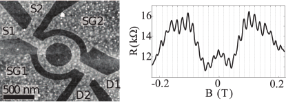
The authors of Ref. Huefner et al., 2009 further speculate on the presence of edge disorder indicated by the fact that the various charge carrier trajectories around the ring, which can be derived from the frequency distribution of the magnetooscillations, do not cover the full area of the ring arms.
Further experiments on graphene ring structures include the local oxidation nanolithography using atomic force microscopy Weng et al. (2008) and antidot arrays on epitaxial graphene films Shen et al. (2008); in the latter setup, universal conductance fluctuations are suppressed since the sample size exceeds the phase coherence length, while Aharonov-Bohm oscillations are still visible due to the small size of the antidots. As a graphene-specific feature, the authors also observe increased visibility of weak localization due to intervalley scattering on antidot edges. Shubnikov-de Haas and Aharonov-Bohm effects on thin graphite single crystals with columnar defects were investigated in Refs. Latyshev et al., 2009, 2010 in a four-probe measurement, and a significant contribution of surface Dirac fermions (“graphene on graphite”) as well as evidence supporting the theoretical prediction of edge states was found. Another multi-terminal measurement of Shubnikov-de Haas oscillations in monolayer graphene relating the Landau level separation between electrons and holes with the transport gap in the density of states is given in Ref. Yoo et al., 2010; the poor visibility of the Aharonov-Bohm oscillations therein is attributed to a low phase coherence length.
Theoretical progress.
On the theoretical side, there is a great variety of topics which have been addressed, including the valley degree of freedom characteristic for graphene, particular device geometries and edge symmetries, resonant behavior and transistor applications, as well as the role of interactions. Common quantities expressing the influence of these aspects include electronic properties such as spectrum and persistent current, as well as transport properties such as conductance and noise.
In the pioneering work on the topic of Aharonov-Bohm rings made of graphene Recher et al. (2007), it was shown—both analytically using a circular ring in the weak intervalley scattering limit in the continuum model, as well as numerically using a hexagonal ring structure with zigzag terminated edges and strong intervalley scattering—that in the confined geometry of a graphene ring structure an applied magnetic flux gives rise to a lifting of the orbital degeneracy in a controllable fashion, which is manifest in conductance and persistent current, even in the absence of intervalley scattering. The magnitude of the lifting of valley degeneracy and it’s dependence on details of the geometry of the ring have subsequently also been discussed in Ref. Yan and Wei, 2010. The effect was further observed in numerical magnetotransport simulations in the closed (or weakly coupled) circular ring geometry described by the tight-binding model Wurm et al. (2010) for the case of smooth mass confinement, where intervalley scattering is suppressed. In this work, simulations have been done both for ballistic and diffusive regimes, and up to the quantum Hall regime where Aharonov-Bohm oscillations are found to be suppressed.
Perfectly shaped ring devices with clean, well defined edges such as the hexagonal ring structure mentioned before Recher et al. (2007) have been addressed in various studies, exploiting graphene-specific features of such ideal nanostructures. A detailed numerical study of the influence of shape and geometry, edge symmetries and corner structures on the electronic structure in the presence of a magnetic field reveals for example the edge state anticrossing and therefore gap opening due to the coupling of states localized at the inner and outer edges of the ring as well as the crucial role of corners in zigzag or armchair edge terminated rings Bahamon et al. (2009). For instance, the corners in an ideal hexagonal ring with zigzag edge termination in a magnetic field introduce intervalley scattering, as was considered in a supercell approach within the tight-binding model Ma et al. (2009); in this work, also a peculiar dependence of the spectrum as well as the persistent current on the even (resulting in semiconducting behavior) or odd (resulting in metallic behavior) character of the number of atoms across the ring arm width was found. Similar rings with metallic armchair termination have been considered in Refs. Luo et al., 2009; Fertig and Brey, 2010; in such systems, appropriately chosen corner junctions exhibit signatures of effective broken time reversal symmetry—caused by pseudomagnetic fields—at low energies, such as broken particle-hole symmetry or a gap in the spectrum that may be closed by the application of a real magnetic flux (The generation of pseudomagnetic fields in graphene rings under strain (or shear stress) has further been discussed in Ref. Abedpour et al., 2011.). In Ref. Ma and Ding, 2010, the authors calculate the spectrum and the persistent current in ideal diamond shaped graphene ring structures either with zigzag or armchair edge termination within the tight-binding model; they also encounter the even-odd behavior mentioned before, and compare their results with previous work on hexagonal rings Ma et al. (2009).
Such ideal structures have also been found to be dominated by resonant behavior in the magnetotransport, for instance in Ref. Wu et al., 2010, where for small rectangular graphene nanorings with perfect edges resonant tunneling through quasi-bound states was observed rather than Aharonov-Bohm oscillations, which may be tuned by varying geometry, Fermi energy, or magnetic field. Resonant behavior was also observed in Ref. Wurm et al., 2010 as well as in in Ref. Munárriz et al., 2011, where it was proposed to utilize the electrostatic Aharonov-Bohm effect via side gates—such as already realized experimentally in Ref. Huefner et al., 2010—for application in a quantum interference transistor with high on/off ratio made of a hexagonal graphene ring structure with perfect edges, where armchair edges were found to be preferable. In contrast, zigzag edges in the leads, acting as valley filters, and a circular graphene ring structure exhibiting an irregular boundary were considered in Ref. Rycerz, 2009, where resonant behavior was encountered as well; however, the main finding of this work was that for opposite valley polarization in the leads and appropriately sized rings exhibiting higher harmonics in the Fourier spectrum due to multiple turns around the ring region, the lowest harmonic is suppressed while higher harmonics are unaffected. A similar geometry, namely a graphene Aharonov-Bohm ring connected to valley filters which encircles a dislocation, was considered in the continuum model in Ref. Mesaros et al., 2009, and decoherence properties were discussed. Possible applications as quantum interference transistors have also recently been discussed in Ref. Xu et al., 2012 for disordered graphene rings, where ballistic rectification and negative differential resistance are observed in the --characteristic; further, while for temperatures as large as mK, phonon scattering is negligible, future work on the effect of electron-phonon interaction might be interesting.
Other aspects of interactions in graphene quantum rings have also been addressed in Ref. Abergel et al., 2008 in the continuum model, with a focus on the interplay between valley polarization and Coulomb interaction, affecting the valley degeneracy. This influence was found to be accessible through the fractional nature of the periodicity of the Aharonov-Bohm oscillations in the persistent current as well as changes in the absorption spectrum. An analysis in the tight-binding model including electron-electron interactions further revealed the connection between electronic correlations and the spin polarization of the interacting ground state as function of ring size and number of electrons Potasz et al. (2009, 2010). The interaction with the electromagnetic field has been discussed in Ref. Moskalenko and Berakdar, 2009, where it was found that, in a graphene ring threaded by a magnetic flux, excitations generated by electromagnetic pulses give rise to “valley currents”—in analogy to spin currents.
The peculiar properties of graphene systems suggest to consider the Aharonov-Bohm effect also in more graphene-specific ring geometries and transport regimes. The electronic properties of monolayer as well as bilayer graphene rings in a magnetic field have been addressed in Refs. Zarenia et al., 2009; Zarenia et al., 2010a, b, either defining the ring geometry by tuning the band gap of bilayer graphene or employing a simplified zero-width ring geometry within the framework of the Dirac equation. In the magnetotransport within the (Andreev-)Corbino disk geometry in graphene, Landau level resonances, the suppression of conductance oscillations away from the charge neutrality point, and the crossover to the normal ballistic transport regime at large doping and weak fields have been encountered Rycerz (2010). Analytical expressions for conductance and Fano factor in the magnetotransport of pseudodiffusive graphene rings, where transport at the Dirac point is dominated by evanescent modes, have been derived in Ref. Katsnelson, 2010.
In the next sections, we will review our previous work on two graphene-specific effects in more detail. In Sec. II, Klein tunneling of Dirac fermions through a potential barrier in a graphene ring system similar to the experimental setup of Refs. Huefner et al., 2009, 2010 is considered. A related effect—Andreev reflection at a graphene-superconductor interface in a mesoscopic ring device—is subsequently discussed in Sec. III. In Sec. IV we will conclude and provide an outlook on potential future developments on the topic of the Aharonov-Bohm effect in graphene.
II Interplay of the Aharonov-Bohm effect and Klein tunneling in graphene
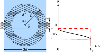
In this section, we review the numerical investigation of the effect of Klein tunneling Katsnelson et al. (2006); Cheianov and Fal’ko (2006) on the Aharonov-Bohm oscillations in a graphene ring on the basis of a tight-binding model with nearest-neighbor couplings. In order to introduce Klein tunneling into the system, an electrostatic potential can be applied to one of the arms of the ring (see Fig. 2 for a schematic), such that this arm together with the two adjacent leads form either a - or -junction (: conduction band transport, : valence band transport).
The former case corresponds to normal tunneling and the latter case to Klein tunneling. Then, the transmission properties strongly depend on the smoothness of the -interfaces. In particular, for sharp junctions the amplitude profile is symmetric around the charge neutrality point in the gated arm, whereas for smooth junctions the Aharonov-Bohm oscillations are strongly suppressed in the Klein tunneling as compared to the normal tunneling regime. Such a setup thus allows for a clear graphene-specific signature in Aharonov-Bohm measurements which seems to be readily observable. Its physical origin is the quantum interference of normal tunneling as well as Klein tunneling trajectories through the two arms of the ring. The work presented in this section was originally published in Ref. Schelter et al., 2010.
II.1 Model
The calculation is based on the usual tight-binding Hamiltonian for graphene
| (1) |
where the second sum runs over nearest-neighbors and is a position-dependent on-site potential, taking the origin of coordinates at the center of the ring. The graphene hopping integral eV picks up a Peierls phase in the presence of a magnetic field, yielding for the nearest-neighbor coupling element the expression
| (2) |
where the line integral is taken along the straight path between sites and . is the magnetic flux quantum, and
| (3) |
with is the vector potential giving rise to a homogeneous magentic field
| (4) |
The system under consideration is a ring-shaped structure cut out of a graphene sheet, which is attached to two crystalline leads also modeled using the graphene lattice structure (see Fig. 2). Besides the magnetic field, the structure is also subject to a gate electrode potential located on top of the lower arm of the ring. The smoothness of the potential interface is controlled via the smoothing width measured from the lower edges of the leads:
In the presented simulations, a cosine-shaped smoothing profile is used and .
For a Fermi energy , together with the adjacent leads this lower arm forms either a - or -junction for and , respectively (see Fig. 3 for a schematic; the Fermi energy is measured relative to the charge neutrality point in the leads).
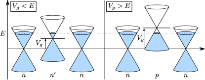
Note that the setup exhibits a flat potential profile for trajectories along the upper ring arm, i. e. a -junction, since there is no gate potential applied. This enables a rather large transmission through the ring even when the lower ring arm is tuned towards the Dirac point, since transport through the upper arm always takes place at an energy distance away from the charge neutrality point.
Transport calculations are done in the Landauer-Büttiker formalism for elastic transport at zero temperature assuming complete phase-coherence using a variant of the recursive Green’s function technique Lee and Fisher (1981); Thouless and Kirkpatrick (1981); MacKinnon (1985) for the coupling of the surface Green’s functions of the leads, as described in Ref. Schelter et al., 2010; the linear conductance of the system is expressed through the transmission function , where is the transmission matrix between the two leads, i. e. the lower left block of the unitary scattering matrix ,
| (5) |
which is obtained from the Green’s function of the coupled system via a Fisher-Lee relation. is the number of propagating modes in the leads.
II.2 Results
In the following, we present transmission properties for a ring with and , nm being the nearest-neighbor distance in graphene, in terms of the linear conductance , where the factor 2 accounts for spin degeneracy. Edge disorder is applied to the ring by randomly removing sites within a width from the inner and outer edges of the ring, respectively (see Fig. 2). We choose in order to keep the edge of the ring as smooth as possible while still allowing for different edge disorder configurations. Fermi energy and gate potential are chosen such that transport always takes place in between the van Hove singularities located at where the density of states diverges in the tight binding model of graphene, , . In Fig. 4, we plot the magnetoconductance at Fermi energy and zero gate voltage () for a particular ring realization, showing pronounced Aharonov-Bohm oscillations on top of a low frequency background.
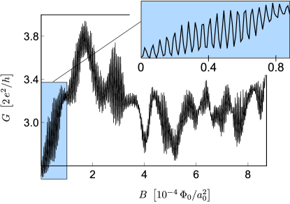
The background signal results from universal conductance fluctuations (UCF) which are typical for phase-coherent mesoscopic devices Datta (2005). The behavior is in agreement with the observations made in Ref. Wurm et al., 2010, where the authors investigate an even wider magnetic field range up to the quantum Hall regime. In Fig. 5, we also show the corresponding frequency spectrum obtained from a Fourier transform of the magnetoconductance signal up to , as well as the UCF background signal and the magnetooscillations after background removal by means of a high pass frequency filter.
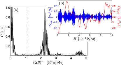
The contributions to the Aharonov-Bohm oscillations are centered around . Using , this frequency corresponds to a mean radius of interfering electron trajectories, which perfectly lies within the boundaries of the ring.
By applying a gate voltage to one of the ring arms, the magnitude of the Aharonov-Bohm oscillations may be modified. A convenient measure of the oscillation magnitude is the root mean square (RMS) amplitude of the signal. Prior to the RMS analysis, the UCF background has to be removed from the signal. This is achieved by applying a high pass frequency filter to the Fourier transform of the magnetoconductance data, as indicated in Fig. 5. The retained, unbiased signal is squared, and the root of the average over the squared signal is defined as the RMS amplitude .
In Fig. 6 we show the dependence of the RMS oscillation amplitude on the gate voltage for different smoothing widths (see Fig. 2) at energy , where the average is taken over the range .
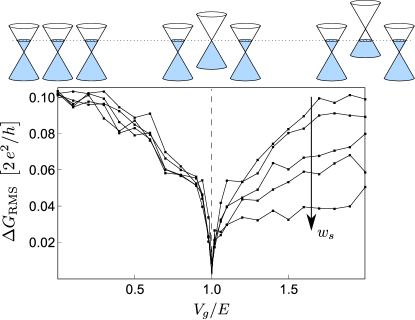
Increasing the gate voltage from zero towards the neutrality point not only leads to increased potential scattering but also to a reduction in the number of accessible propagating states in the lower arm of the ring. As can be seen in Fig. 6, the oscillation amplitude diminishes and reaches a minimum value at the neutrality point. Note that, since the transmission through the upper ring arm is not at all affected by a gate potential, the overall conductance itself is only slightly changed to fluctuate around (see Fig. 7 in Ref. Schelter et al., 2010) as compared to values around in the case of zero gate potential on the lower ring arm (see Fig. 4).
For , the decay of the RMS amplitude towards the neutrality point does not depend on the details of the gate potential interface. However, in the regime of Klein tunneling, , the oscillation behavior strongly depends on the smoothness of the gate potential. In case of a smooth potential, the partial waves in the lower arm have to tunnel through a finite region of low density of states, where (see Fig. 2), in order to interfere with the partial waves traversing the upper arm. The lower arm becomes increasingly penetrable as this region gets narrower, until it gets transparent in case of a sharp potential. This reflects the usual behavior of Klein tunneling phenomena, where the probability for tunneling through a -junction depends on the smoothness of the -interface Beenakker (2008); Cheianov and Fal’ko (2006).
The described behavior of the RMS amplitude is robust over the whole energy range under consideration, except for an increasing uncertainty at lower values for the Fermi energy. Although all results are presented for zigzag boundary conditions in the leads, the effects are independent of a change of orientation of the graphene lattice to armchair boundaries in the leads.
Klein tunneling in graphene thus exhibits clear signatures in the Aharonov-Bohm oscillations observed in mesoscopic rings. In the next section, we will show how another graphene-specific effect, namely specular Andreev reflection at a graphene-superconductor interface Beenakker (2006), can be identified in such nanostructures.
III How to distinguish specular from retro Andreev reflection in graphene rings
In this section, we review numerical transport calculations of Andreev reflection in a graphene ring system threaded by a magnetic flux and attached to one normal conducting and one superconducting lead. To this end, the Bogoliubov-de Gennes equation for the tight binding model using the recursive Green’s functions technique is solved within the Landauer-Büttiker framework for elastic transport. By tuning chemical potential and bias voltage, it is possible to switch between regimes where electron and hole originate from the same band (retro configuration) or from different bands (specular configuration) of the graphene dispersion, respectively. Andreev reflection is known to be closely related to the effect of Klein tunneling discussed in the previous section. Beenakker et al. (2008) However, different aspects of Klein tunneling have become experimentally accessible in the last years Stander et al. (2009); Young and Kim (2009), whereas specular Andreev reflection has not been observed to date, although there exist a number of proposals for the experimental control Cheng et al. (2009) and detection Beenakker (2006); Titov et al. (2007); Cheng et al. (2011) of this process. (For a review on both effects, see Ref. Beenakker, 2008.) Here, we review a novel approach concerning the identification of specular Andreev reflection, distinguishing it from conventional retro reflection, and discuss the advantages over previous works in the field. We find that the dominant contributions to the Aharonov-Bohm oscillations in the subgap transport are of period in retro configuration, whereas in specular configuration they are of period . This result confirms the predictions obtained from a qualitative analysis of interfering scattering paths, and since it is robust against disorder and moderate changes of the system, it provides a clear signature to distinguish both types of Andreev reflection processes in graphene. The work presented in this section was originally published in Ref. Schelter et al., 2012.
III.1 Scattering path analysis
Our approach is based on the observation, that in general, the probability for an incident electron to be reflected as a hole is less than one. This allows for effects typical for phase-coherent mesoscopic devices, like universal conductance fluctuations or Aharonov-Bohm oscillations Aharonov and Bohm (1959) in the magnetoconductance. While in normal metals, the fundamental period of these oscillations is given by the flux quantum , it is half the value for Andreev (retro) reflection in conventional metals, due to the charge of a Cooper pair. However, this is not true anymore in the case of specular Andreev reflection, therefore providing a criterion to distinguish between specular and retro reflection. In order to show this, we consider the phases due to the magnetic flux that are picked up by the various scattering paths. In this analysis, we restrict ourselves to the contributions up to first order in the sense that we take processes into account that involve only a single electron-hole conversion process, and that contain at most one additional round-trip of electron or hole, respectively; higher order contributions connected with additional round-trips are often times negligible Schelter et al. (2010); Russo et al. (2008). The corresponding paths are summarized in Fig. 7.
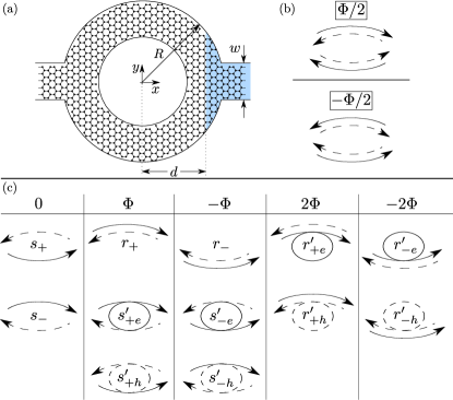
In order to obtain the magnetoconductance for the two types of Andreev reflection, we sum up the amplitudes as defined in Fig. 7 for the various paths coherently:
where , , and is the magnetic flux measured in units of the flux quantum . Assuming for any zeroth- and first-order amplitudes, respectively, we obtain
| (6) |
where and contains contributions that are constant with respect to . Therefore, in the case of specular reflection, oscillations of period are dominant. In contrast, in the case of retro reflection, contributions of period are dominant, as expected:
| (7) |
where again contains -independent terms and we assume for any zeroth- and first-order amplitudes, respectively.
III.2 Numerical model
In order to test the previous analysis on the basis of a microscopic model, we implement the Bogoliubov-de Gennes Hamiltonian Gennes (1999)
| (8) |
within the tight binding formalism of graphene, Eq. (1). In this numerical calculation, all higher order contributions beyond the ones discussed in the previous subsection are also taken into account. In Eq. (8), we assume for the superconducting order parameter . The presence of a magnetic field is captured by a Peierls phase in the hopping matrix element, Eq. (2).
The structure of the graphene device under consideration is schematically shown in Fig. 7. The two semi-infinite leads also exhibit the graphene lattice structure; superconductivity is induced into the right lead due to the proximity effect of a superconducting electrode on top of the graphene. We choose to orient the leads to exhibit armchair edges and later comment on the reason for this particular choice. The whole ring is penetrated by a uniform perpendicular magnetic field of strength , described by the vector potential (3). The origin of coordinates is taken at the center of the ring.
In order to fulfill the mean-field requirement of superconductivity, which demands the superconducting coherence length to be large compared to the wavelength in the superconducting region Beenakker (2006), we introduce additional doping into the superconducting region by applying a gate potential . Which type of Andreev reflection occurs at the NS interface is then determined by the excitation energy (i. e. the eigenvalues of Eq. (8)) and the Fermi energy , as shown in Fig. 8.
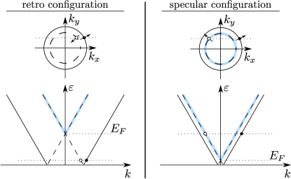
In retro configuration, , where for the -components of the electron and hole velocities, both electron and hole traverse the same arm of the ring. In specular configuration, , the hole is reflected back through the other arm of the ring, since . In the following, we choose , justifying the adoption of the step-function model for the superconducting order parameter, Beenakker (2006).
In order to compare retro (r) and specular (s) configurations, we will choose and since then the states in both configurations exhibit the same wavelength and there is the same number of propagating modes. We further choose so that for nearly each value of , there exist electron-hole scattering channels.
Again, the transport properties of the system are obtained from the scattering matrix that is calculated in the framework of the Landauer-Büttiker formalism using the recursive Green’s function technique as in the previous section. In the framework of the Bogoliubov-de Gennes Hamiltonian, Green’s function and scattering matrix are parameterized by the eigenvalues of the Hamiltonian (8).
In the following, we will concentrate on the regime , in which there are no propagating modes in the superconducting lead, so that electrons injected from the normal conducting lead are reflected back either as electron (e) or hole (h). The scattering matrix thus has the structure
from which the differential conductance for the Andreev processes is given by
where the factor 4 accounts for spin degeneracy and the quantization of charge in units of .
III.3 Results
In Fig. 9, we show the calculated transmission for a ring of width and outer radius , where is the distance between nearest neighbors.
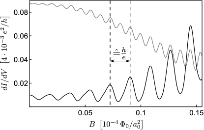
The transmission function exhibits Aharonov-Bohm oscillations on top of a low frequency background which is due to universal conductance fluctuations. The position of the NS interface is given by . The chosen dimensions of the ring are large enough to exclude finite-size effects while still being numerically manageable. For the superconducting order parameter, we choose a value of meV, which may appear unrealistic at first sight, considered the fact that typical values are up to a few meV. However, by making this choice we scale the value of the superconducting order parameter according to the scale of the system size, such that the dimensionless factor stays of same order of magnitude, compared with values realized in experiments Russo et al. (2008); Huefner et al. (2010). Thus, for a realistic system size of m, our choice of would correspond to a value of a few meV for the superconducting gap. Note that due to these low energy scales and the rather large spacing of modes resulting from the narrow geometry of the electron waveguides in such a ring structure, in specular configuration only the regime of a low number of modes is accessible. Also note that due to strong electron backscattering at the front of the hole and at the rough edges of the ring, the average value of the differential conductance is much less than a conductance quantum, .
The average radius of the scattering path is calculated according to , where () in specular (retro) configuration and is the (dominant) period of the oscillation. Evaluating the period of the oscillations shown in Fig. 9, we obtain in specular configuration and in retro configuration. The obtained values lie well within the inner and outer radius of the ring and close to the arithmetic mean , therefore confirming the predictions obtained from Eqs. (6) and (7). Minor contributions of period in retro configuration and in specular configuration visible in Fig. 9 may arise due to terms neglected in Eqs. (6) and (7), scattering off the sharp boundaries of the ring structure, and the fact that for the electron-hole conversion at the NS interface is not strictly conserved.
Another strong evidence that supports our interpretation of the two different periods is the breakdown of this particular signature that is observed for a shift of the position of the NS interface on the scale of the width of the ring. Indeed, while in Ref. Haugen et al., 2010—where a three-terminal graphene junction is analyzed—the exact position of the NS interface has no effect, it matters here; the reason is that is comparable or even less than the system size, while in Ref. Haugen et al., 2010 the superconducting coherence length greatly exceeds the system dimensions. If the interface is too close to the hole region (see Fig. 10 (a) inset), then specularly reflected holes are forced to traverse the same arm as the incoming electron.
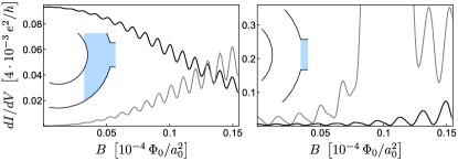
In this case, one should observe oscillations in specular configuration. In contrast, if the interface is too far from the hole (see Fig. 10 (b) inset), holes may significantly be reflected through the other arm, e. g. due to increased scattering at the ring boundaries. This would manifest itself in the observation of oscillations in addition to the oscillations in retro configuration. This behavior is confirmed in the observed magnetooscillations, as shown in Fig. 10.
Apart from that, the vs. signature proves to be very robust against moderate changes to the length and energy scales in the system, such as the extent of the magnetic field or the ratio of Fermi wavelength and the width of the NS interface. We also tested that the signature persists when more propagating modes are present in the lead, leading to values of the average conductance which are much larger compared to the few-mode situation shown in Fig. 9 (see Fig. 11).
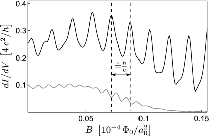
Additionally, the signature is hardly affected by bulk disorder, which is a major advantage of our setup. In Fig. 12, we show the magnetoconductance of the system used in Fig. 9 with a particular random short-range disorder configuration, which is realized by applying an uncorrelated, random on-site potential of Gaussian distribution with zero mean and width to each site.

In addition, the NS interface has been smeared out over a distance in this case. The robustness of the effect can be explained from the topological nature of the signature: since all microscopic scattering paths can be classified into just two groups—yielding - or -oscillations, respectively—according to which arm is traversed by the quasiparticles, impurity scattering and the resulting deflection of quasiparticles has no adverse effect as long as scattering between the groups is weak, while scattering within one group may be arbitrarily strong. In addition, note that while our description of transport via the scattering matrix assumes complete phase coherence, a signature that distinguishes retro from specular Andreev reflection is assumed to persist also in the case of a finite phase coherence length. More specifically, if the phase coherence length is on the order of the ring circumference, first-order amplitudes in Eqs. (6) and (7) may be neglected. Then, retroreflection would still manifest itself in -oscillations, while there would be no oscillations at all in the case of specular reflection.
Finally, we add a remark concerning the choice of armchair boundary conditions in the leads employed in the analysis in this section. In a tight binding implementation of graphene, there are two simple choices for the orientation of the leads. Often, zigzag edges are considered to represent a generic boundary condition for graphene ribbons Akhmerov and Beenakker (2008). In this case, edge states are present in the system that modify the simple picture provided in Fig. 8 by adding additional scattering channels between bulk and edge states while removing certain scattering channels between bulk states due to the conservation of the so-called pseudoparity symmetry that acts like a selection rule Rainis et al. (2009). In the realistic limit of metal leads providing a large number of propagating bulk modes, this effect should be less important. However, for the system geometry used in the numerical calculations in combination with the low energy scales, it may significantly affect the observed behavior. In order to avoid this influence, we chose armchair boundary conditions in the leads that do not provide any edge states. Note in addition, that in realistic systems the zigzag-specific effect would also be suppressed since the zigzag edge state is not protected against disorder when next-nearest neighbor hopping is taken into account Wimmer (2009). Therefore, we are convinced that our results based on armchair edges in the reservoirs describe the generic situation for wide leads.
IV Conclusions and outlook
Considering the development of the topic of the Aharonov-Bohm effect in graphene, we can assess that there is a great variety of aspects covered by theoretical considerations, and despite the significant amount of work done on graphene ring systems, there are still a number of open questions drawn from initial experiments that remain unanswered so far, as well as a large number of theoretical predictions not yet confirmed by corresponding experiments. On the one hand, it would be interesting from a theoretical point of view to investigate the origin and significance of the seemingly linear relationship between conductance and oscillation amplitude as well as the significant increase of the oscillation amplitude at high magnetic field observed in Ref. Russo et al., 2008. Further analysis on the role of interactions may also be worthwhile. On the other hand, while some of the theoretical models are hardly realizable in experiments at the present stage e. g. due to insufficient control over edge properties, there are systems, such as presented in the previous two sections, that should be experimentally accessible and robust, and should therefore allow for the observation of graphene-specific features in the Aharonov-Bohm effect.
Acknowledgements.
We acknowledge interesting discussions and collaborations on the subject with C. W. J. Beenakker, Y. M. Blanter, D. Bohr, C. Bruder, F. Dolcini, K. Ensslin, A. F. Morpurgo, A. Rycerz, C. Stampfer, and M. Wimmer. We further thank the DFG and the ESF for financial support.References
- Ehrenberg and Siday (1949) W. Ehrenberg and R. E. Siday, Proceedings of the Physical Society. Section B 62, 8 (1949).
- Aharonov and Bohm (1959) Y. Aharonov and D. Bohm, Phys. Rev. 115, 485 (1959).
- Aharonov and Bohm (1961) Y. Aharonov and D. Bohm, Phys. Rev. 123, 1511 (1961).
- Toland and Search (2010) J. R. Toland and C. P. Search, Physics Letters A 374, 923 (2010).
- Webb et al. (1985) R. A. Webb, S. Washburn, C. P. Umbach, and R. B. Laibowitz, Phys. Rev. Lett. 54, 2696 (1985).
- Bachtold et al. (1999) A. Bachtold, C. Strunk, J.-P. Salvetat, J.-M. Bonard, L. Forro, T. Nussbaumer, and C. Schönenberger, Nature 397, 673 (1999).
- Novoselov et al. (2004) K. S. Novoselov, A. K. Geim, S. V. Morozov, D. Jiang, Y. Zhang, S. V. Dubonos, I. V. Grigorieva, and A. A. Firsov, Science 306, 666 (2004).
- Novoselov et al. (2005) K. S. Novoselov, A. K. Geim, S. V. Morozov, D. Jiang, M. I. Katsnelson, I. V. Grigorieva, S. V. Dubonos, and A. A. Firsov, Nature 438, 197 (2005).
- Zhang et al. (2005) Y. Zhang, Y.-W. Tan, H. L. Stormer, and P. Kim, Nature 438, 201 (2005).
- Geim and Novoselov (2007) A. K. Geim and K. S. Novoselov, Nat Mater 6, 183 (2007).
- Beenakker (2008) C. W. J. Beenakker, Rev. Mod. Phys. 80, 1337 (2008).
- Castro Neto et al. (2009) A. H. Castro Neto, F. Guinea, N. M. R. Peres, K. S. Novoselov, and A. K. Geim, Rev. Mod. Phys. 81, 109 (2009).
- Russo et al. (2008) S. Russo, J. B. Oostinga, D. Wehenkel, H. B. Heersche, S. S. Sobhani, L. M. K. Vandersypen, and A. F. Morpurgo, Phys. Rev. B 77, 085413 (2008).
- Washburn and Webb (1986) S. Washburn and R. A. Webb, Advances in Physics 35, 375 (1986).
- Angers et al. (2007) L. Angers, E. Zakka-Bajjani, R. Deblock, S. Guéron, H. Bouchiat, A. Cavanna, U. Gennser, and M. Polianski, Phys. Rev. B 75, 115309 (2007).
- Huefner et al. (2009) M. Huefner, F. Molitor, A. Jacobsen, A. Pioda, C. Stampfer, K. Ensslin, and T. Ihn, physica status solidi (b) 246, 2756 (2009).
- Wurm et al. (2010) J. Wurm, M. Wimmer, H. U. Baranger, and K. Richter, Semiconductor Science and Technology 25, 034003 (2010).
- Huefner et al. (2010) M. Huefner, F. Molitor, A. Jacobsen, A. Pioda, C. Stampfer, K. Ensslin, and T. Ihn, New Journal of Physics 12, 043054 (2010).
- Weng et al. (2008) L. Weng, L. Zhang, Y. P. Chen, and L. P. Rokhinson, Applied Physics Letters 93, 093107 (2008).
- Shen et al. (2008) T. Shen, Y. Q. Wu, M. A. Capano, L. P. Rokhinson, L. W. Engel, and P. D. Ye, Appl. Phys. Lett. 93, 122102 (2008).
- Latyshev et al. (2009) Y. Latyshev, A. Latyshev, A. Orlov, A. Shchekin, V. Bykov, P. Monceau, K. van der Beck, M. Kontsikovskii, and I. Monnet, JETP Letters 90, 480 (2009).
- Latyshev et al. (2010) Y. U. I. Latyshev, A. P. Orlov, E. G. Shustin, N. V. Isaev, W. Escoffier, P. Monceau, C. J. van der Beek, M. Konczykowski, and I. Monnet, Journal of Physics: Conference Series 248, 012001 (2010).
- Yoo et al. (2010) J. S. Yoo, Y. W. Park, V. Skakalova, and S. Roth, Applied Physics Letters 96, 143112 (2010).
- Recher et al. (2007) P. Recher, B. Trauzettel, A. Rycerz, Y. M. Blanter, C. W. J. Beenakker, and A. F. Morpurgo, Phys. Rev. B 76, 235404 (2007).
- Yan and Wei (2010) C.-H. Yan and L.-F. Wei, Journal of Physics: Condensed Matter 22, 295503 (2010).
- Bahamon et al. (2009) D. A. Bahamon, A. L. C. Pereira, and P. A. Schulz, Phys. Rev. B 79, 125414 (2009).
- Ma et al. (2009) M. M. Ma, J. W. Ding, and N. Xu, Nanoscale 1, 387 (2009).
- Luo et al. (2009) T. Luo, A. P. Iyengar, H. A. Fertig, and L. Brey, Phys. Rev. B 80, 165310 (2009).
- Fertig and Brey (2010) H. A. Fertig and L. Brey, Philosophical Transactions of the Royal Society A: Mathematical, Physical and Engineering Sciences 368, 5483 (2010).
- Abedpour et al. (2011) N. Abedpour, R. Asgari, and F. Guinea, Phys. Rev. B 84, 115437 (2011).
- Ma and Ding (2010) M. Ma and J. Ding, Solid State Communications 150, 1196 (2010).
- Wu et al. (2010) Z. Wu, Z. Z. Zhang, K. Chang, and F. M. Peeters, Nanotechnology 21, 185201 (2010).
- Munárriz et al. (2011) J. Munárriz, F. Domínguez-Adame, and A. V. Malyshev, Nanotechnology 22, 365201 (2011).
- Rycerz (2009) A. Rycerz, Acta Physica Polonica A 115, 322 (2009).
- Mesaros et al. (2009) A. Mesaros, D. Sadri, and J. Zaanen, Phys. Rev. B 79, 155111 (2009).
- Xu et al. (2012) N. Xu, J. Ding, B. Wang, D. Shi, and H. Sun, Physica B: Condensed Matter 407, 335 (2012).
- Abergel et al. (2008) D. S. L. Abergel, V. M. Apalkov, and T. Chakraborty, Phys. Rev. B 78, 193405 (2008).
- Potasz et al. (2009) P. Potasz, A. D. Güçlü, and P. Hawrylak, Acta Physica Polonica A 116, 832 (2009).
- Potasz et al. (2010) P. Potasz, A. D. Güçlü, and P. Hawrylak, Phys. Rev. B 82, 075425 (2010).
- Moskalenko and Berakdar (2009) A. S. Moskalenko and J. Berakdar, Phys. Rev. B 80, 193407 (2009).
- Zarenia et al. (2009) M. Zarenia, J. M. Pereira, F. M. Peeters, and G. A. Farias, Nano Lett. 9, 4088 (2009).
- Zarenia et al. (2010a) M. Zarenia, J. M. Pereira, A. Chaves, F. M. Peeters, and G. A. Farias, Phys. Rev. B 81, 045431 (2010a).
- Zarenia et al. (2010b) M. Zarenia, J. M. Pereira, A. Chaves, F. M. Peeters, and G. A. Farias, Phys. Rev. B 82, 119906 (2010b).
- Rycerz (2010) A. Rycerz, Phys. Rev. B 81, 121404 (2010).
- Katsnelson (2010) M. I. Katsnelson, Eur. Phys. Lett. 89, 17001 (2010).
- Katsnelson et al. (2006) M. I. Katsnelson, K. S. Novoselov, and A. K. Geim, Nat. Phys. 2, 620 (2006).
- Cheianov and Fal’ko (2006) V. V. Cheianov and V. I. Fal’ko, Phys. Rev. B 74, 041403 (2006).
- Schelter et al. (2010) J. Schelter, D. Bohr, and B. Trauzettel, Phys. Rev. B 81, 195441 (2010).
- Lee and Fisher (1981) P. A. Lee and D. S. Fisher, Phys. Rev. Lett. 47, 882 (1981).
- Thouless and Kirkpatrick (1981) D. J. Thouless and S. Kirkpatrick, Journal of Physics C: Solid State Physics 14, 235 (1981).
- MacKinnon (1985) A. MacKinnon, Zeitschrift für Physik B Condensed Matter 59, 385 (1985).
- Datta (2005) S. Datta, Electronic transport in mesoscopic systems, Cambridge studies in semiconductor physics and microelectronic engineering (Cambridge University Press, 2005).
- Beenakker (2006) C. W. J. Beenakker, Phys. Rev. Lett. 97, 067007 (2006).
- Beenakker et al. (2008) C. W. J. Beenakker, A. R. Akhmerov, P. Recher, and J. Tworzydło, Phys. Rev. B 77, 075409 (2008).
- Stander et al. (2009) N. Stander, B. Huard, and D. Goldhaber-Gordon, Phys. Rev. Lett. 102, 026807 (2009).
- Young and Kim (2009) A. F. Young and P. Kim, Nat. Phys. 5, 222 (2009).
- Cheng et al. (2009) S.-g. Cheng, Y. Xing, J. Wang, and Q.-f. Sun, Phys. Rev. Lett. 103, 167003 (2009).
- Titov et al. (2007) M. Titov, A. Ossipov, and C. W. J. Beenakker, Phys. Rev. B 75, 045417 (2007).
- Cheng et al. (2011) S.-G. Cheng, H. Zhang, and Q.-F. Sun, Phys. Rev. B 83, 235403 (2011).
- Schelter et al. (2012) J. Schelter, B. Trauzettel, and P. Recher, arXiv:1110.4383; accepted for publication in Phys. Rev. Lett. (2012).
- Gennes (1999) P. G. D. Gennes, Superconductivity Of Metals And Alloys, Advanced book classics (Westview Press, 1999).
- Haugen et al. (2010) H. Haugen, D. Huertas-Hernando, A. Brataas, and X. Waintal, Phys. Rev. B 81, 174523 (2010).
- Akhmerov and Beenakker (2008) A. R. Akhmerov and C. W. J. Beenakker, Phys. Rev. B 77, 085423 (2008).
- Rainis et al. (2009) D. Rainis, F. Taddei, F. Dolcini, M. Polini, and R. Fazio, Phys. Rev. B 79, 115131 (2009).
- Wimmer (2009) M. Wimmer, Ph.D. thesis, Regensburg (2009).