First-principles study of the phonon-limited mobility in -type single-layer MoS2
Abstract
In the present work we calculate the phonon-limited mobility in intrinsic -type single-layer MoS2 as a function of carrier density and temperature for K. Using a first-principles approach for the calculation of the electron-phonon interaction, the deformation potentials and Fröhlich interaction in the isolated MoS2 layer are determined. We find that the calculated room-temperature mobility of cm2 V-1 s-1 is dominated by optical phonon scattering via deformation potential couplings and the Fröhlich interaction with the deformation potentials to the intravalley homopolar and intervalley longitudinal optical phonons given by eV/cm and eV/cm, respectively. The mobility is weakly dependent on the carrier density and follows a temperature dependence with at room temperature. It is shown that a quenching of the characteristic homopolar mode which is likely to occur in top-gated samples, boosts the mobility with cm2 V-1 s-1 and can be observed as a decrease in the exponent to . Our findings indicate that the intrinsic phonon-limited mobility is approached in samples where a high- dielectric that effectively screens charge impurities is used as gate oxide.
pacs:
81.05.Hd, 72.10.-d, 72.20.-i, 72.80.JcI Introduction
Alongside with the rise of graphene and the exploration of its unique electronic properties Geim and Novoselov (2007); Neto et al. (2009); Sarma et al. (2011), the search for other two-dimensional (2D) materials with promising electronic properties has gained increased interest Neto and Novoselov (2011). Metal dichalcogenides which are layered materials similar to graphite, provide interesting candidates. Their layered structure with weak interlayer van der Waals bonds allows for fabrication of single- to few-layer samples using mechanical peeling/cleavage or chemical exfoliation techniques similar to the fabrication of graphene Novoselov et al. (2005); Ayari et al. (2007); Matte et al. (2010); Radisavljevic et al. (2011). However, in contrast to graphene they are semiconductors and hence come with a naturally occurring band gap—a property essential for electronic applications.
The vibrational and optical properties of single- to few-layer samples of MoS2 have recently been studied extensively using various experimental techniques Lee et al. (2010); Mak et al. (2010); Korn et al. (2011). In contrast to the bulk material which has an indirect-gap, it has been demonstrated that single-layer MoS2 is a direct-gap semiconductor with a gap of eV Mak et al. (2010); Splendiani et al. (2010). Together with the excellent electrostatic control inherent of two-dimensional materials, the large band gap makes it well-suited for low power applications Yoon et al. (2011). So far, electrical characterizations of single-layer MoS2 have shown -type conductivity with room-temperature mobilities in the range cm2 V-1 s-1 Novoselov et al. (2005); Ayari et al. (2007); Radisavljevic et al. (2011). Compared to early studies of the intralayer mobility of bulk MoS2 where mobilities in the range cm2 V-1 s-1 were reported Fivaz and Mooser (1967), this is rather low. In a recent experiment the use of a high- gate dielectric in a top-gated device was shown to boost the carrier mobility to a value of 200 cm2 V-1 s-1 Radisavljevic et al. (2011). The observed increase in the mobility was attributed to screening of impurities by the high- dielectric and/or modifications of MoS2 phonons in the top-gated sample.
In order to shed further light on the measured mobilities and the possible role of phonon damping due to a top-gate dielectric Radisavljevic et al. (2011), we have carried out a detailed study of the phonon-limited mobility in single-layer MoS2. Since phonon scattering is an intrinsic scattering mechanism that often dominates at room temperature, the theoretically predicted phonon-limited mobility sets an upper limit for the experimentally achievable mobilities in single-layer MoS2 Hwang and Sarma (2008). In experimental situations, the temperature dependence of the mobility can be useful for the identification of dominating scattering mechanisms and also help to establish the value of the intrinsic electron-phonon couplings Kawamura and Sarma (1990). However, the existence of additional extrinsic scattering mechanisms often complicates the interpretation. For example, in graphene samples impurity scattering and scattering on surface polar optical phonons of the gate oxide are important mobility-limiting factors Hwang et al. (2007); Nomura and MacDonald (2007); Chen et al. (2008); Konar et al. (2010); Li et al. (2010); Heo et al. (2011). It can therefore be difficult to establish the value and nature of the intrinsic electron-phonon interaction from experiments alone. Theoretical studies therefore provide useful information for the interpretation of experimentally measured mobilities.
In the present work, the electron-phonon interaction in single-layer MoS2 is calculated from first-principles using a density-functional based approach. From the calculated electron-phonon couplings, the acoustic (ADP) and optical deformation potentials (ODP) and the Fröhlich interaction in single-layer MoS2 are inferred. Using these as inputs in the Boltzmann equation, the phonon-limited mobility is calculated in the high-temperature regime ( K) where phonon scattering often dominate the mobility. Our findings demonstrate that the calculated phonon-limited room-temperature mobility of cm2 V-1 s-1 is dominated by optical deformation potential and polar optical scattering via the Fröhlich interaction. The dominating deformation potentials of eV/cm and eV/cm originate from the couplings to the homopolar and the intervalley polar LO phonon. This is in contrast to previous studies for bulk MoS2, where the mobility has been assumed to be dominated entirely by scattering on the homopolar mode Fivaz and Mooser (1967); Fivaz (1969); Schmid (1974). Furthermore, we show that a quenching of the characteristic homopolar mode which is polarized in the direction normal to the MoS2 layer can be observed as a change in the exponent of the generic temperature dependence of the mobility. Such a quenching can be expected to occur in top-gated samples where the MoS2 layer is sandwiched between a substrate and a gate oxide.
The paper is organized as follows. In Section II the band structure and phonon dispersion of single-layer MoS2 as obtained with DFT-LDA are presented. The latter is required for the calculation of the electron-phonon coupling presented in Section III. From the calculated electron-phonon couplings, we extract zero- and first-order deformation potentials for both intra and intervalley phonons. In addition, the coupling constant for the Fröhlich interaction with the polar LO phonon is determined. In Section IV, the calculation of the phonon-limited mobility within the Boltzmann equation is outlined. This includes a detailed treatment of the phonon collision integral from which the scattering rates for the different coupling mechanisms can be extracted. In Section V we present the calculated mobilities as a function of carrier density and temperature. Finally, in Section VI we summarize and discuss our findings.
II Electronic structure and phonon dispersion
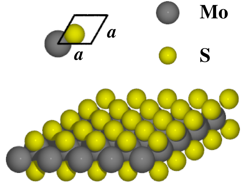
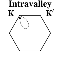
The electronic structure and phonon dispersion of single-layer MoS2 have been calculated within DFT in the LDA approximation using a real-space projector-augmented wave (PAW) method Mortensen et al. (2005); Larsen et al. (2009); Enkovaara et al. (2010). The equilibrium lattice constant of the hexagonal unit cell shown in Fig. 1 was found to be Å using a -point sampling of the Brillouin zone. In order to eliminate interactions between the layers due to periodic boundary conditions, a large interlayer distance of 10 Å has been used in the calculations.
II.1 Band structure
In the present study, the band structure of single-layer MoS2 is calculated within DFT-LDA Lebègue and Eriksson (2009); Han et al. (2011). While DFT-LDA in general underestimates band gaps, the resulting dispersion of individual bands, i.e. effective masses and energy differences between valleys, is less problematic. We note, however, that recent GW quasi-particle calculations which in general give a better description of the band structure in standard semiconductors Aulbur et al. (2000), suggest that the distance between the -valleys and the satellite valleys located on the - path inside the Brillouin zone not as large as predicted by DFT (see below) and that the valley ordering may even be inverted Ataca and Ciraci (2011); Olsen et al. (2011). This, however, seems to contradict with the experimental consensus that single-layer MoS2 is a direct-gap semiconductor Mak et al. (2010); Splendiani et al. (2010) and further studies are needed to clarify this issue. In the following we therefore use the DFT-LDA band structure and comment on the possible consequences of a valley inversion in Section VI.
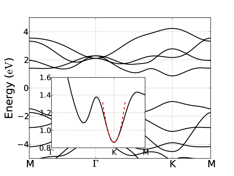
The calculated DFT-LDA band structure is shown in Fig. 2. It predicts a direct band gap of eV at the -poing in the Brillouin zone. The inset shows a zoom of the bottom of the conduction band along the -K-M path in the Brillouin zone. As demonstrated by the dashed line, the conduction band is perfectly parabolic in the -valley. Furthermore, the satellite valley positioned on the path between the -point and the -point lies on the order of meV above the conduction band edge and is therefore not relevant for the low-field transport.
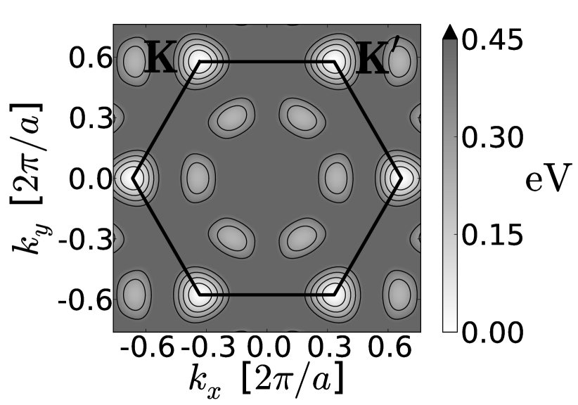
The right plot in Fig. 1 shows a contour plot of the lowest lying conduction band valleys in the two-dimensional Brillouin zone. Here, the -valleys that are populated in -type MoS2, are positioned at the corners of the hexagonal Brillouin zone. Due to their isotropic and parabolic nature, the part of the conduction band relevant for the low-field mobility can to a good approximation be described by simple parabolic bands
| (1) |
with an effective electron mass of and where is measured with respect to the -points in the Brillouin zone. The two-dimensional nature of the carriers is reflected in the constant density of states given by where and are the spin and -valley degeneracy, respectively. The large density of states which follows from the high effective mass of the conduction band in the -valleys, results in non-degenerate carrier distributions except for very high carrier densities.
II.2 Phonon dispersion
The phonon dispersion has been obtained with the supercell-based small-displacement method Alfé (2009) using a supercell. The resulting phonon dispersion shown in Fig. 3 is in excellent agreement with recent calculations of the lattice dynamics in two-dimensional MoS2 Ataca et al. (2011).
With three atoms in the unit cell, single-layer MoS2 has nine phonon branches—three acoustic and six optical branches. Of the three acoustic branches, the frequency of the out-of-plane flexural mode is quadratic in for . In the long-wavelength limit, the frequency of the remaining transverse acoustic (TA) and longitudinal acoustic (LA) modes are given by the in-plane sound velocity as
| (2) |
Here, the sound velocity is found to be and m/s for the TA and LA mode, respectively.
The gap in the phonon dispersion completely separates the acoustic and optical branches even at the high-symmetry points at the zone-boundary where the acoustic and optical modes become similar. The two lowest optical branches belong to the non-polar optical modes. Due to an insignificant coupling to the charge carriers, they are not relevant for the present study.
The next two branches with a phonon energy of meV at the -point are the transverse (TO) and longitudinal (LO) polar optical modes where the Mo and S atoms vibrate in counterphase. In bulk polar materials, the coupling of the lattice to the macroscopic polarization setup by the lattice vibration of the polar LO mode results in the so-called LO-TO splitting between the two modes in the long-wavelength limit. The inclusion of this effect from first-principles requires knowledge of the Born effective charges Giannozzi et al. (1991); Gonze and Lee (1997); Wang et al. (2010). In two-dimensional materials, however, the lack of periodicity in the direction perpendicular to the layer removes the LO-TO splitting Sánchez-Portal and Hernández (2002). The coupling to the macroscopic polarization of the LO mode will therefore be neglected here.
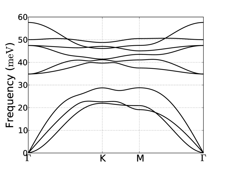
The almost dispersionless phonon at meV is the so-called homopolar mode which is characteristic for layered structures. The lattice vibration of this mode corresponds to a change in the layer thickness and has the sulfur layers vibrating in counterphase in the direction normal to the layer plane while the Mo layer remains stationary. The change in the potential associated with this lattice vibration has previously been demonstrated to result in a large deformation potential in bulk MoS2 Fivaz and Mooser (1967).
III Electron-phonon coupling
In this section, we present the electron-phonon coupling in single-layer MoS2 obtained with a first-principles based DFT approach. The method is based on a supercell approach analogous to that used for the calculation of the phonon dispersion and is outlined in App. A. The calculated electron-phonon couplings are discussed in the context of deformation potential couplings and the Fröhlich interaction well-known from the semiconductor literature.
Within the adiabatic approximation for the electron-phonon interaction, the coupling strength for the phonon mode with wave vector and branch index is given by
| (3) |
where is the phonon frequency, is an appropriately defined effective mass, is the number of unit cells in the crystal, and
| (4) |
is the coupling matrix element where is the wave vector of the carrier being scattered and is the change in the effective potential per unit displacement along the vibrational normal mode.
Due to the valley degeneracy in the conduction band, both intra and intervalley phonon scattering of the carriers in the -valleys need to be considered. Here, the coupling constants for these scattering processes are approximated by the electron-phonon coupling at the bottom of the valleys, i.e. with . With this approach, the intra and intervalley scattering for the -valleys are thus assumed independent on the wave vector of the carriers.
In the following two sections, the calculated electron-phonon couplings are presented foo (a). The different deformation potential couplings are discussed and the functional form of the Fröhlich interaction in 2D materials is established. Piezoelectric coupling to the acoustic phonons which occurs in materials without inversion symmetry, is most important at low temperatures Kawamura and Sarma (1992) and will not be considered here. As deformation potentials are often extracted as empirical parameters from experimental mobilities, it can be difficult to disentangle contributions from different phonons. Here, the first-principles calculation of the electron-phonon coupling allows for a detailed analysis of the couplings and to assign deformation potentials to the individual intra and intervalley phonons.
III.1 Deformation potentials
The deformation potential interaction describes how carriers interact with the local changes in the crystal potential associated with a lattice vibration. Within the deformation potential approximation, the electron-phonon coupling is expressed as Ferry (2000)
| (5) |
where is the area of the sample, is the atomic mass density per area and is the coupling matrix element for a given valley which is assumed independent on the -vector of the carriers. This expression follows from the general definition of the electron-phonon coupling in Eq. 3 by setting the effective mass equal to the sum of the atomic masses in the unit cell. With this convention for the effective mass, , and the expression in Eq. (5) is obtained.
For scattering on acoustic phonons, the coupling matrix element is linear in in the long-wavelength limit,
| (6) |
where is the acoustic deformation potential.
In the case of optical phonon scattering, both coupling to zero- and first-order in must be considered. The interaction via the constant zero-order optical deformation potential is given by
| (7) |
The coupling via the zero-order deformation potential is dictated by selection rules for the coupling matrix elements. Therefore, only symmetry-allowed phonons can couple to the carriers via the zero-order interaction. The coupling via the first-order interaction is given by Eq. (6) with the acoustic deformation potential replaced by the first-order optical deformation potential . Both the zero- and first-order deformation potential coupling can give rise to intra and intervalley scattering.
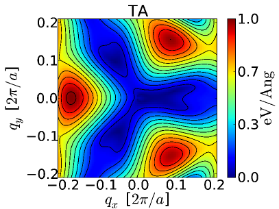
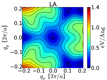
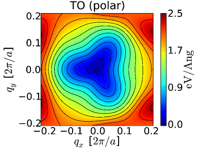
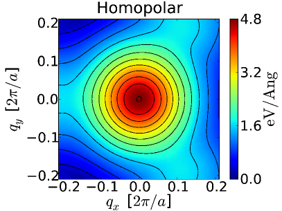
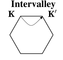
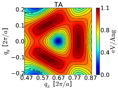
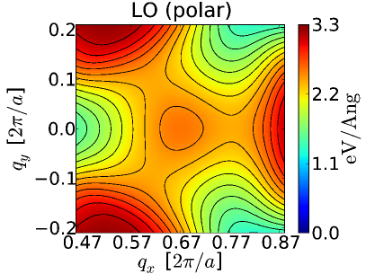
The absolute value of the calculated coupling matrix elements are shown in Fig. 4 for phonons which couple to the carriers via deformation potential interactions. They are plotted in the range of phonon wave vectors relevant for intra and intervalley scattering processes foo (b), and only phonon modes with significant coupling strengths have been included. Although the coupling matrix elements are shown only for , the matrix elements for are related through time-reversal symmetry as . The three-fold rotational symmetry of the coupling matrix elements in -space stems from the symmetry of the conduction band in the vicinity of the -valleys (see Fig. 1). Since the symmetry of the matrix elements has not been imposed by hand, slight deviations from the three-fold rotational symmetry can be observed.
The acoustic deformation potential couplings for the TA and LA modes are shown in the two top plots of Fig. 4. Due to the inclusion of Umklapp processes here, the coupling to the TA mode does not vanish as is most often assumed Madelung (1996). Only along high-symmetry directions in the Brillouin zone is this the case. This results in a highly anisotropic coupling to the TA mode. On the other hand, the deformation potential coupling for the LA mode is perfectly isotropic in the long-wavelength limit but also becomes anisotropic at shorter wavelengths. In agreement with Eq. (6), both the TA and LA coupling matrix elements are linear in in the long-wavelength limit.
The next two plots show the couplings to the intravalley polar TO and homopolar optical modes. While the interaction with the polar TO phonon corresponds to a first-order optical deformation potential, the interaction with the homopolar mode acquires a finite value of eV/Å in the -point and corresponds to a strong zero-order deformation potential coupling. The large deformation potential coupling to the homopolar mode stems from its characteristic lattice vibration polarized in the direction perpendicular to the layer corresponding to a change in the layer thickness. The associated change in the effective potential from the counterphase oscillation of the two negatively charged sulfur layers results in a significant change of the potential towards the center of the MoS2 layer. As the electronic Bloch functions have significant weight here, the homopolar lattice vibration gives rise to a significant shift of the -valley states. The large deformation potential associated with the coupling to the homopolar mode is also present in bulk MoS2 Fivaz and Mooser (1967).
The two bottom plots in Fig. 4 show the couplings for the intervalley TA and polar LO phonons. Due to the nearly constant frequency of the intervalley acoustic phonons, their couplings are classified as optical deformation potentials in the following. Both the shown coupling to the intervalley TA phonon and the coupling to the intervalley LA phonon result in first-order deformation potentials. The intervalley coupling for the polar LO phonon gives rise to a zero-order deformation potential which results from an identical in-plane motion of the two sulfur layers in the lattice vibration of the intervalley phonon.
In general, the deformation potential approximation, i.e. the assumption of isotropic and constant/linear coupling matrix elements, in Eqs. (6) and (7) is seen to hold in the long-wavelength limit only. At shorter wavelengths, the first-principles couplings become anisotropic and have a more complicated -dependence. When determined experimentally from e.g. the temperature dependence of the mobility Kawamura and Sarma (1990), the deformation potentials in Eqs. (6) and (7) implicitly account for the more complex -dependence of the true coupling matrix element. In Section V, the theoretical deformation potentials for single-layer MoS2 are determined from the first-principles electron-phonon couplings. This is done by fitting their associated scattering rates to the scattering rates obtained with the first-principles coupling matrix elements. The resulting the deformation potentials, can be used in practical transport calculations based on e.g. the Boltzmann equation or Monte Carlo simulations. It should be noted that similar routes for first-principles calculations of deformation potentials have been given in the literature Sjakste et al. (2006); Tyuterev et al. (2010); Borysenko et al. (2010).
III.2 Fröhlich interaction
The lattice vibration of the polar LO phonon gives rise to a macroscopic electric field that couples to the charge carriers. For bulk three-dimensional systems, the coupling to the field is given by the Fröhlich interaction which diverges as in the long-wavelength limit Madelung (1996),
| (8) |
where is the vacuum permittivity, is the volume of the sample , and and are the high-frequency optical and static dielectric constant, respectively.
In atomically thin materials, the two-dimensional nature of both the LO phonon and the charge carriers leads to a qualitatively different -dependence of the Fröhlich interaction. The situation is similar to 2D semiconductor heterostructures where the Fröhlich interaction has been studied using dielectric continuum models and microscopic based approaches Mori and Ando (1989); Rücker et al. (1992). From the microscopic considerations presented in App. B, we derive the following functional form for the Fröhlich interaction to the polar LO phonon in 2D materials,
| (9) |
Here, the coupling constant is the equivalent of the square root factors in Eq. (8), is the effective width of the electronic Bloch states and erfc is the complementary error function.
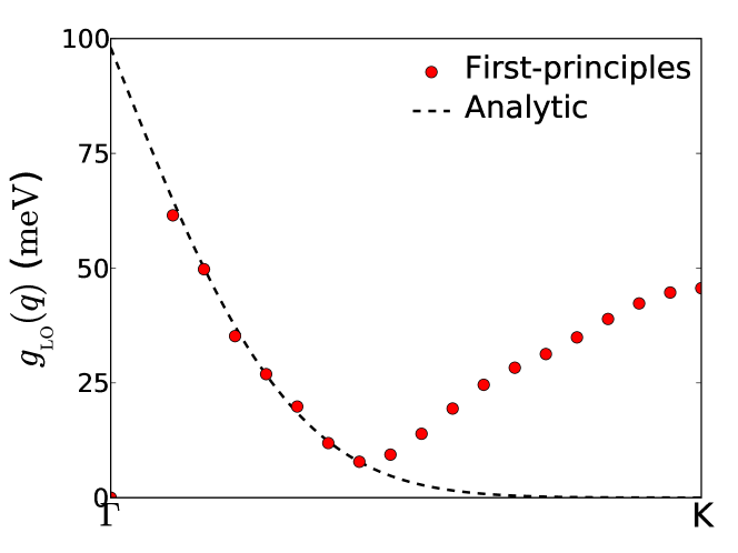
Figure 5 shows the first-principles coupling to the polar LO phonon in single-layer MoS2 (dots) as a function of the phonon wave vector along the - path. The dashed line shows a fit of the coupling in Eq. (9) to the long-wavelength limit of the calculated coupling. With a coupling constant of meV and an effective width of Å, the analytic form gives a perfect description of the calculated coupling in the long-wavelength limit. For shorter wavelengths, the zero-order deformation potential coupling to the intervalley LO phonon from Fig. 4 becomes dominant, and a deviation away from the behavior in Eq. (9) is observed.
IV Boltzmann equation
In the regime of diffuse transport dominated by phonon scattering, the mobility can be obtained with semiclassical Boltzmann transport theory. In the absence of spatial gradients the Boltzmann equation for the out-of-equilibrium distribution function of the charge carriers reads Smith and Jensen (1989)
| (10) |
where the time evolution of the crystal momentum is governed by and is the charge of the carriers. In the case of a time-independent uniform electric field, the steady-state version of the linearized Boltzmann equation takes the form
| (11) |
where is the equilibrium Fermi-Dirac distribution function, , and is the band velocity. In linear response, the out-of-equilibrium distribution function can be written as the equilibrium function plus a small deviation away from its equilibrium value Smith and Jensen (1989), i.e.
| (12) |
Here, the last equality has defined the deviation function . Furthermore, following the spirit of the iterative method of Rode Rode (1975), the angular dependence of the deviation function is separated out as
| (13) |
where is the angle between the -vector and the force exerted on the carriers by the applied field . In general, is a function of the -vector and not only its magnitude . However, for isotropic bands as considered here, the angular dependence of the deviation function is entirely accounted for by the cosine factor in Eq. (13) Ferry (2000).
Considering the phonon scattering, the collision integral describes how accelerated carriers are driven back towards their equilibrium distribution by scattering on acoustic and optical phonons. In the high-temperature regime of interest here, the collision integral can be split up in two contributions. The first, accounting for the quasielastic scattering on acoustic phonons, can be expressed in the form of a relaxation time . The second, describing the inelastic scattering on optical phonons, will in general be an integral operator . The collision integral can thus be written
| (14) |
where the explicit forms of the relaxation time and the integral operator will be considered in detail below.
With the above form of the collision integral, the Boltzmann equation can be solved by iterating the equation
| (15) |
for the deviation function . Here, the angular dependence and a factor have been divided out and the new integral operator is defined by
| (16) |
From the solution of the Boltzmann equation the current and drift mobility of the carriers can be obtained. Taking the electric field to be oriented along the -direction, the current density is given by
| (17) |
where is the conductivity, is the area of the sample, and is the band velocity for parabolic bands with . From the definition of the drift mobility, it follows that
| (18) |
where the modified deviation function having units of time is defined by
| (19) |
and the energy-weighted average is defined by
| (20) |
Here, is the two-dimensional carrier density. In the relaxation time approximation and the well-known Drude expression for the mobility is recovered.
IV.1 Phonon collision integral
The phonon collision integral has been considered in great detail in the literature for two-dimensional electron gases in semiconductor heterostructure (see e.g. Ref. Kawamura and Sarma, 1992). In general, these treatments consider scattering on three-dimensional or quasi two-dimensional phonons. In atomically thin materials the phonons are strictly two-dimensional which results in a slightly different treatment. In the following, a full account of the two-dimensional phonon collision integral is given for scattering on acoustic and optical phonons.
With the distribution function written on the form in Eq. (12), the linearized collision integral for electron-phonon scattering takes the form Smith and Jensen (1989)
| (21) |
where is the equilibrium distribution of the phonons given by the Bose-Einstein distribution function and is understood. The different terms inside the square brackets account for scattering out of () and into () the state with wave vector via absorption and emission of phonons. Screening of the electron-phonon interaction by the carriers themselves is accounted for by the static dielectric function , which is both wave vector and temperature dependent. Due to the large effective mass of the conduction band, the charge carriers in single-layer MoS2 are non-degenerate except at very high carrier concentrations. Semiclassical screening where the screening length is given by the inverse of the Debye-Hückel wave vector therefore applies Ferry and Goodnick (2009). For the considered values of carrier densities and temperatures, this corresponds to a small fraction of the size of the Brillouin zone, i.e. . As scattering on phonons in general involves larger wave vectors, screening by the carriers can to a good approximation be neglected here. The calculated mobilities therefore provide a lower limit for the proper screened mobility.
IV.1.1 Quasielastic scattering on acoustic phonons
For quasielastic scattering on acoustic phonons at high temperatures, the energy of the acoustic phonon can be neglected in the collision integral in Eq. (IV.1). As a consequence, the collision integral can be recast in the form of the following relaxation time Kawamura and Sarma (1992)
| (22) |
where the summation variable has been changed to and the transition matrix element for quasielastic scattering on acoustic phonons is given by
| (23) |
For isotropic scattering as assumed here in Eq. (6), the square of the electron-phonon coupling can be expressed as
| (24) |
where the acoustic phonon frequency has been expressed in terms of the sound velocity . Except at very low temperatures implying that the equipartition approximation for the Bose-Einstein distribution applies. With the resulting -factors in the transition matrix element in Eq. (IV.1.1) canceling, the in the -sum in Eq. (22) vanishes and the first term yields a factor density of states divided by the spin and valley degeneracies . The relaxation time for acoustic phonon scattering becomes
| (25) |
The independence on the carrier energy and the temperature dependence of the acoustic scattering rate are characteristic for charge carriers in two-dimensional heterostructures and layered materials Fivaz and Mooser (1967); Kawamura and Sarma (1992).
IV.1.2 Inelastic scattering on dispersionless optical phonons
For inelastic scattering on optical phonons the phonon energy can no longer be neglected and the collision integral in Eq. (IV.1) must be considered in full detail. Under the reasonable assumption of dispersionless optical phonons , the inelastic collision integral can be treated semianalytically. The overall procedure for the evaluation of the collision integral is given below, while the calculational details have been collected in App. C. The resulting expressions for the collision integral apply to both intravalley and intervalley optical and intervalley acoustic phonons.
In the following, the integral operator for inelastic scattering in Eq. (16) is split up in separate out- and in-scattering contributions,
| (26) |
which include the terms in Eq. (IV.1) involving and , respectively. With the contributions from different phonon branches adding up, scattering on a single phonon with branch index is considered in the following.
From Eq. (IV.1), the out-scattering part of the collision integral follows directly as
| (27) |
where the transition matrix element for optical phonon scattering is given by
| (28) |
For the in-scattering part, the desired factor in Eq. (16) can be extracted from using the relation . Since the sine term vanishes from symmetry consideration, the in-scattering part of the inelastic collision integral reduces to
| (29) |
The evaluation of the -sum in Eqs. (27) and (29) is outlined in App. C. Here, the assumption of dispersionless optical phonons allows for an semianalytical treatment. For zero- and first-order coupling within the deformation potential approximation, the sum can be carried out analytically. The resulting expressions for the collision integral are given in Eqs. (C.2.1), (65), (C.2.2), (67) and (C.2.2). In the case of the Fröhlich interaction, the angular part of the -integral must be done numerically.
IV.1.3 Optical deformation potential scattering rates
In spite of the fact that the collision integral for inelastic scattering on optical phonons cannot be recast in the form of a (momentum) relaxation time foo (c), a scattering rate related to the inverse carrier lifetime can still be defined from the out-scattering part of the inelastic collision integral alone. The scattering rate so defined is given by
| (30) |
and corresponds to the imaginary part of the electronic self-energy in the Born approximation Smith and Jensen (1989). Below, the resulting scattering rates for zero-order and first-order deformation potential scattering are given for non-degenerate carriers, i.e. with the Fermi factors in Eq. (30) neglected. They follow straight-forwardly from the expressions for the out-scattering part of the collision integral derived in App. C. It should be noted that the scattering rate for the zero-order deformation potential interaction given below in Eq. (31), in fact defines a proper momentum relaxation time because the in-scattering part of the collision integral vanishes in this case (see App. C).
For zero-order deformation potential scattering, the scattering rate is independent of the carrier energy and given by
| (31) |
Here, is the Heavyside step function which assures that only electrons with sufficient energy can emit a phonon.
The scattering rate for coupling via the first-order deformation potential is found to be
| (32) |
Due to the linear dependence on the carrier energy, zero-order scattering processes dominate first-order processes at low energies. Only under high-field conditions where the carriers are accelerated to high velocities will first-order scattering become significant.
The expressions for the scattering rates in Eqs. (31) and (IV.1.3) above apply to scattering on dispersionless intervalley acoustic phonons and intra/intervalley optical phonons. Except for a factor of originating from the density of states, the energy dependence of the scattering rates is identical to that of their three-dimensional analogs Ferry (2000).
V Results
In the following, the scattering rate and phonon-limited mobility in single-layer MoS2 are studied as a function of carrier energy, temperature and carrier density using the material parameters collected in Tab. 1. Here, the reported deformation potentials represent effective coupling parameters for the deformation potential approximation in Eqs. (6) and (7) (see below).
| Parameter | Symbol | Value |
|---|---|---|
| Lattice constant | 3.14 Å | |
| Ion mass density | g/cm2 | |
| Effective electron mass | 0.48 | |
| Transverse sound velocity | m/s | |
| Longitudinal sound velocity | m/s | |
| Acoustic deformation potentials | ||
| TA | eV | |
| LA | eV | |
| Optical deformation potentials | ||
| TA | eV | |
| LA | eV | |
| TO | eV | |
| TO | eV | |
| LO | eV/cm | |
| Homopolar | eV/cm | |
| Fröhlich interaction (LO) | ||
| Effective layer thickness | 4.41 Å | |
| Coupling constant | meV | |
| Optical phonon energies | ||
| Polar LO | 48 meV | |
| Homopolar | 50 meV |
V.1 Scattering rates
With access to the first-principles electron-phonon couplings, the scattering rate taking into account the anisotropy and more complex -dependence of the first-principles coupling matrix elements can be evaluated. They are obtained using the expression for the scattering rate in Eq. (30) with the respective transition matrix elements for acoustic and optical phonon scattering given in Eqs. (IV.1.1) and (IV.1.2) foo (d). In order to account for the different coupling matrix elements in the -valleys, the scattering rates have been averaged over different high-symmetry directions of the carrier wave vector . The resulting scattering rates are shown in Fig. 6 as a function of the carrier energy for non-degenerate carriers at K. The different lines show the contributions to the total scattering rate from the various electron-phonon couplings to the intra and intervalley phonons which have been grouped according to their coupling type, i.e. acoustic deformation potentials (ADPs), zero/first-order optical deformation potentials (ODPs) and the Fröhlich interaction. The acoustic deformation potential scattering includes the quasielastic intravalley scattering on the TA and LA phonons with linear dispersions. Scattering on intervalley acoustic phonons is considered as optical deformation potential scattering. Both the total scattering rate and the contributions from the different coupling types have been obtained using Matthiessen’s rule by summing the scattering rates from the individual phonons, i.e.
| (33) |
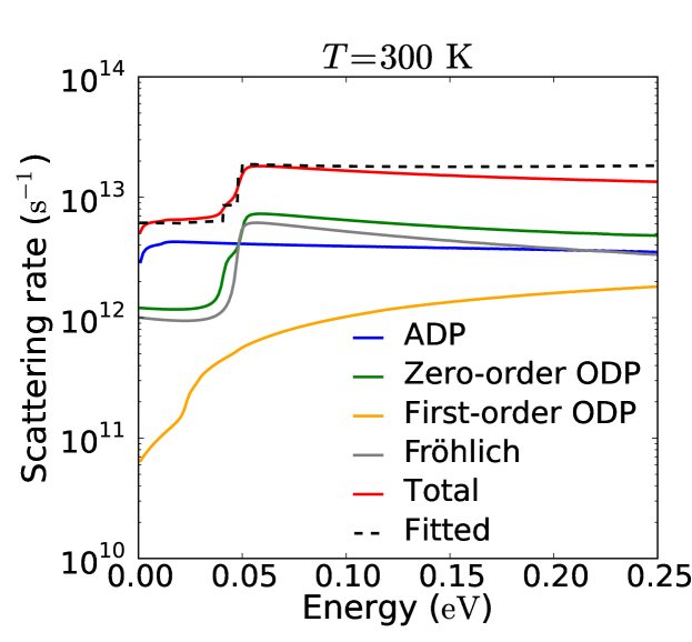
For carrier energies below the optical phonon frequencies, the total scattering rate is dominated by acoustic deformation potential scattering. At higher energies zero-order deformation potential scattering and polar optical scattering via the Fröhlich interaction become dominant. Due to the linear dependence on the carrier energy, the first-order deformation potential scattering on the intervalley acoustic phonons and the optical phonons is in general only of minor importance for the low-field mobility. This is also the case here, where it is an order of magnitude smaller than the other scattering rates for almost the entire plotted energy range. The jumps in the curves for the optical scattering rates at the optical phonon energies are associated with the threshold for optical phonon emission where the carriers have sufficient energy to emit optical phonons
V.2 Deformation potentials
In this section, we determine the deformation potential parameters in single-layer MoS2. They can be used in the following study of the low-field mobility within the Boltzmann approach outlined in Section IV.
The energy dependence of the first-principles based scattering rates in Fig. 6 to a high degree resembles that of the analytic expressions for the deformation potential scattering rates in Eqs. (25), (31) and (IV.1.3). For example, the acoustic and zero-order deformation potential scattering rates are almost constant in the plotted energy range. The first-principles electron-phonon couplings can therefore to a good approximation be described by the simpler isotropic deformation potentials in Eqs. (6) and (7). The deformation potentials are obtained by fitting the associated scattering rates for each of the intra and intervalley phonons separately to the first-principles scattering rates. The resulting deformation potential values are summarized in Tab. 1. In analogy with deformation potentials extracted from experimental mobilities, the theoretical deformation potentials represent effective coupling parameters that implicitly account for the anisotropy and the full -dependence of the first-principles electron-phonon couplings. However, as momentum and energy conservation limit phonon scattering to involve phonons in the vicinity of the -point foo (b), the fitting procedure yields deformation potentials close to the direction averaged / limiting behavior of the first-principles coupling matrix elements. For the zero-order deformation potentials, the sampling of the coupling matrix elements away from the -point in the sum in Eq. (30), leads to a deformation potentials which is slightly smaller than the -point value of the coupling matrix element.
The total scattering rate resulting from the fitted deformation potentials is shown in Fig. 6 to give an almost excellent description of the first-principles scattering rate. With the mobility in the relaxation time approximation given by the energy-weighted average of the relaxation time (see Eq. (18)), the difference between the associated mobilities will be negligible. Hence, the deformation potentials provide well-founded electron-phonon coupling parameters for low-field studies of the mobility.
V.3 Mobility
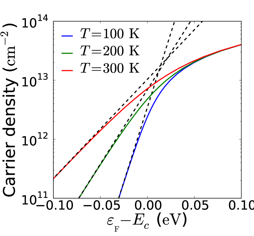
The high density of states in the -valleys of the conduction band in general results in non-degenerate carrier distributions in single-layer MoS2. This is illustrated in the left plot of Fig. 7 which shows the carrier density versus the position of the Fermi level for different temperatures. At room temperature, carrier densities in excess of cm-2 are needed to introduce the Fermi level into the conduction band and probe the Fermi-Dirac statistics of the carriers. Thus, only at the highest reported carrier densities of cm-2 Novoselov et al. (2005), are the carriers degenerate at room temperature. For the lowest temperature K, the transition to degenerate carriers occurs at a carrier density of cm-2. The transition from non-degenerate to degenerate distributions is also illustrated by the discrepancy between the full and dashed lines which shows the Fermi level obtained with Boltzmann statistics.
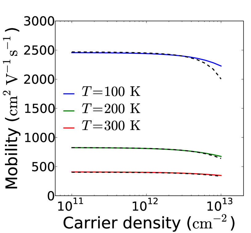
The right plot of Fig. 7 shows the phonon-limited drift mobility calculated with the full collision integral as a function of carrier density for the same set of temperatures. The dashed lines represent the results obtained with Boltzmann statistics and the relaxation time approximation using the expressions in Section IV for optical phonon scattering and Matthiessen’s rule for the total relaxation time. The strong drop in the mobility from cm2 V-1 s-1 at K to cm2 V-1 s-1 at K, is a consequence of the increased phonon scattering at higher temperatures due to larger phonon population of, in particular, optical phonons. The relatively low intrinsic room-temperature mobility of single-layer MoS2 can be attributed to both the significant phonon scattering and the large effective mass of in the conduction band. While the mobility decreases strongly with increasing temperature, it is relatively independent on the carrier density. The weak density dependence of the mobility originates from the energy-weighted average in Eq. (20) where the derivative of the Fermi-Dirac distribution changes slowly as a function of carrier density for non-degenerate carriers. As the Fermi energy is introduced into the band with increasing carrier density, the derivative of the Fermi-Dirac distribution to a larger extent probes the scattering rate at higher energies leading to a decrease of the mobility. This effect is most prominent at K where the level of degeneracy is larger compared to higher temperatures.
Surprisingly, the relaxation time approximation is seen to work extremely well. The deviation from the full treatment at high carrier densities stems from the assumption of non-degenerate carriers and not the relaxation time approximation. The reason for the good performance of the relaxation time approximation shall be found in the in-scattering part of the collision integral in the full treatment. As the in-scattering part of the collision integral vanishes for zero-order deformation potential coupling and is small compared to the out-scattering part otherwise, the full collision integral does not differ significantly from the corresponding scattering rate as defined in Eq. (30) of Section IV, i.e. with the in-scattering part neglected. The good performance of the relaxation time approximation therefore seems to be of general validity for the phonon collision integral even in the presence inelastic scattering on optical phonons.
Finally, we study the temperature dependence of the mobility in more detail. In general, room temperature mobilities are to a large extent dominated by optical phonon scattering. This is manifested in the temperature dependence of the mobility which follows a law where the exponent depends on the dominating scattering mechanism. For acoustic phonon scattering above the Bloch-Grüneisen temperature, the temperature dependence of the scattering rate in Eq. (25) results in . At higher temperatures where optical phonon scattering starts to dominate, the mobility acquires a stronger temperature dependence with . In this regime, the exponent depends on the optical phonon frequencies and the electron-phonon coupling strength. In an early study of the in-plane mobility of bulk MoS2 Fivaz and Mooser (1967), the measured room-temperature exponent of was found to be consistent with scattering on the homopolar mode via a zero-order deformation potential.
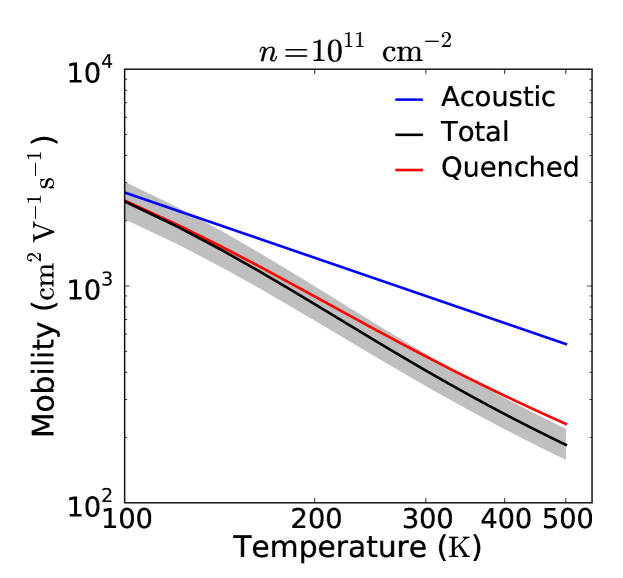
In Fig. 8, we show the temperature dependence of the mobility at cm-2 calculated with the full collision integral. For comparison, the mobility limited by acoustic phonon scattering with the temperature dependence is also included. To illustrate the effect of an uncertainty in the calculated deformation potentials, the shaded area shows the variation of the mobility with a change in the deformation potentials of . The calculated room-temperature mobility of cm2 V-1 s-1 is in fair agreement with the recently reported experimental value of cm2 V-1 s-1 in the top-gated sample of Ref. Radisavljevic et al., 2011 where additional scattering mechanisms as e.g. impurity and surface-optical phonon scattering must be expected to exist. Over the plotted temperature range, the mobility undergoes a transition from being dominated by acoustic phonon scattering at K to being dominated by optical phonon scattering at higher temperatures with a characteristic exponent of . At room temperature, the mobility follows a temperature dependence with . The increase in the exponent is almost exclusively due to the optical zero-order deformation potential couplings and the Fröhlich interaction while the first-order deformation potential couplings contribute only marginally. The exponent found here is considerably lower than the above-mentioned exponent of for bulk MoS2, indicating that the electron-phonon coupling in bulk and single-layer MoS2 differ. Indeed, the transition from an indirect band gap in bulk MoS2 to a direct band gap in single-layer MoS2 which shifts the bottom of the conduction band from the valley located along the -K path to the -valleys, could result in a change in the electron-phonon coupling.
In top-gated samples as the one studied in Ref. Radisavljevic et al., 2011, the sandwiched structure with the MoS2 layer located between substrate and gate dielectric, is likely to result in a quenching of the characteristic homopolar mode which is polarized in the direction normal to the layer. To address the consequence of such a quenching, the mobility in the absence of the zero-order deformation potential originating from the coupling to homopolar mode is also shown in Fig. 8. Here, the curve for the quenched case shows a decrease in the characteristic exponent to and an increase in the mobility of cm2 V-1 s-1 at room temperature. Despite the significant deformation potential of the homopolar mode, the effect of the quenching on the mobility is minor.
VI Discussions and conclusions
Based on our finding for the phonon-limited mobility in single-layer MoS2, it seems likely that the low experimental mobilities of cm2 V-1 s-1 reported in Refs. Novoselov et al., 2005; Ayari et al., 2007; Radisavljevic et al., 2011 are dominated by other scattering mechanisms as e.g. charged impurity scattering. The main reason for the increase in the mobility to 200 cm2 V-1 s-1 observed when depositing a high- dielectric on top of the MoS2 layer in Ref. Radisavljevic et al., 2011 is therefore likely to be impurity screening. The quenching of the out-of-plane homopolar phonon only led to a minor increase in the mobility and cannot alone explain the above-mentioned increase in the mobility. It may, however, also contribute. A comparison of the temperature dependence of the mobility in samples with and without the top-gate structure can help to clarify the extent to which a quenching of optical phonons contributes to the experimentally observed mobility increase. With our theoretically predicted room-temperature mobility of 410 cm2 V-1 s-1, the observed enhancement in the mobility to 200 cm2 V-1 s-1 induced by the high- dielectric, suggests that dielectric engineering Jena and Konar (2007) is an effective route towards phonon-limited mobilities in 2D materials via efficient screening of charge impurities.
A rough estimate of the impurity concentrations required to dominate phonon scattering can be inferred from the phonon scattering rate of s-1 in Fig. 6. The scattering rate is related to the mean-free path of the carriers via where is their mean velocity. Using the velocity of the mean energy carriers for a non-degenerate distribution where , we find a mean-free path of nm at K. In order for impurity scattering to dominate, the impurity spacing must be on the order of the phonon mean-free path or smaller. This results in a minimum impurity concentration of cm-2 in order to dominate phonon scattering. The high value of the estimated impurity concentration needed to dominate phonon scattering is in agreement with the experimental observation that low-mobility single-layer MoS2 samples are heavily doped semiconductors Novoselov et al. (2005).
As discussed in Section II, independent GW quasi-particle calculations Ataca and Ciraci (2011); Olsen et al. (2011) suggest that the ordering of the valleys at the bottom of the conduction band might not be as clear as predicted by DFT. If this is the case, the satellite valleys inside the Brillouin zone must also be taken into account in the solution of Boltzmann equation. This gives rise to additional intervalley scattering channels that together with the larger average effective electron mass of the satellite valley will result in mobilities below the values predicted here.
In conclusion, we have used a first-principles based approach to establish the strength and nature of the electron-phonon coupling and calculate the intrinsic phonon-limited mobility in single-layer MoS2. The calculated room-temperature mobility of 410 cm2 V-1 s-1 is to a large extent dominated by optical deformation potential scattering on the intravalley homopolar and intervalley LO phonons as well as polar optical scattering on the intravalley LO phonon via the Fröhlich interaction. The mobility follows a temperature dependence at room temperature characteristic of optical phonon scattering. A quenching of the homopolar mode likely to occur in top-gated samples, results in a change of the exponent in the temperature dependence of the mobility to 1.52. With effective masses, phonons and measured mobilities in other semiconducting metal dichalcogenides being similar to those of MoS2 Fivaz and Mooser (1967); Fivaz (1969), room-temperature mobilities of the same order of magnitude can be expected in their single-layer forms.
Acknowledgements.
The authors would like to thank O. Hansen and J. J. Mortensen for illuminating discussions. KK has been partially supported by the Center on Nanostructuring for Efficient Energy Conversion (CNEEC) at Stanford University, an Energy Frontier Research Center funded by the U.S. Department of Energy, Office of Science, Office of Basic Energy Sciences under Award Number DE-SC0001060. CAMD is supported by the Lundbeck Foundation.Appendix A First-principles calculation of the electron-phonon interaction
The first-principles scheme for the calculation of the electron-phonon interaction used in this work is outlined in the following. Contrary to other first-principles approaches for the calculation of the electron-phonon interaction which are based on pseudo potentials Sjakste et al. (2006); Giustino et al. (2007); Tyuterev et al. (2010); Borysenko et al. (2010), the present approach is based on the PAW method Blöchl (1994) and is implemented in the GPAW DFT package Mortensen et al. (2005); Larsen et al. (2009); Enkovaara et al. (2010).
Within the adiabatic approximation for the electron-phonon interaction, the electron-phonon coupling matrix elements for the phonon and Bloch state can be expressed as
| (34) |
where is the number of unit cells, is an appropriately defined effective mass, is the phonon frequency, and the -dependent derivative of the effective potential for a given atom is defined by
| (35) |
where the sum is over unit cells in the system and is the gradient of the potential with respect to the position of atom in cell . The polarization vectors of the phonons appearing in Eq. (34) are normalized according to .
In order to evaluate the matrix element in Eq. (34), the Bloch states are expanded in LCAO basis orbitals where is a composite index for atomic site and orbital index and is the lattice vector to the ’th unit cell. In the LCAO basis, the Bloch states are expanded as where
| (36) |
are Bloch sums of the localized orbitals. Inserting the Bloch sum expansion of the Bloch states in the matrix element in Eq. (34), the matrix element can be written
| (37) |
where the -labels on the expansion coefficients have been discarded for brevity. The phase factor from the reciprocal lattice vector can be neglected since . By exploiting the translational invariance of the crystal the matrix elements can be obtained from the gradient in the primitive cell as
| (38) |
by performing the change of variables in the integration. Inserting in Eq. (A) and changing the summing variables to and we find for the matrix element
| (39) |
Here, the sum over in the first equality produces a factor of . The result for the matrix element in Eq. (A) is similar to the matrix element reported in Eq. (22) of Ref. Giustino et al., 2007 where a Wannier basis was used instead of the LCAO basis.
From the last equality in Eq. (A), the procedure for a supercell-based evaluation of the matrix element has emerged. The matrix element in the last equality involves the gradients of the effective potential with respect to atomic displacement in the reference cell at . These can be obtained using a finite-difference approximation for the gradient where the individual components are obtained as
| (40) |
Here, denotes the effective potential with atom located at in the reference cell displaced by in direction . The calculation of the gradient thus amounts to carrying out self-consistent calculations for six displacements of each atom in the primitive unit cell. Having obtained the gradients of the effective potential, the matrix elements in the LCAO basis of the supercell must be calculated and the sums over unit cells and atomic orbitals in Eq. (A) can be evaluated.
In general, the matrix elements of the electron-phonon interaction must be converged with respect to the supercell size and the LCAO basis. In particular, since the supercell approach relies on the gradient of the effective potential going to zero at the supercell boundaries, the supercell must be chosen large enough that the potential at the boundaries is negligible. For polar materials where the coupling to the polar LO phonon is long-ranged in nature, a correct description of the coupling can only be obtained for phonon wave vectors corresponding to wavelengths smaller than the supercell size. Large supercells are therefore required to capture the long-wavelength limit of the coupling constant (see e.g. main text).
A.1 PAW details
In the PAW method, the effective single-particle DFT Hamiltonian is given by
| (41) |
where the first term is the kinetic energy, is the effective potential containing contributions from the atomic potentials and the Hartree and exchange-correlation potentials and the last term is the non-local part including the atom-centered projector functions and the atomic coefficients . In contrast to pseudo-potential methods where the atomic coefficients are constants, they depend on the density and thereby also on the atomic positions in the PAW method.
The diagonal matrix elements (i.e. ) in Eq. (A) correspond to the first-order variation in the band energy upon an atomic displacement in the normal mode direction . Together with the matrix elements for , these can be obtained from the gradient of the PAW Hamiltonian with respect to atomic displacements. The derivative of (41) with respect to a displacement of atom in direction results in the following four terms
| (42) |
While the gradient of the projector functions in the first and second terms inside the square brackets can be evaluated analytically, the gradients of the effective potential and the projector coefficients in the last term are obtained using the finite-difference approximation in Eq. (40).
Once the gradient of the PAW Hamiltonian has been obtained, the matrix elements in Eq. (A) can be obtained. Under the assumption that the smooth pseudo Bloch wave functions from the PAW formalism is a good approximation to the true quasi particle wave function, the matrix element follows as
| (43) |
where is given in Eq. (35). With the pseudo wave function expanded in an LCAO basis, the matrix element is evaluated following Eq. (A).
In order to verify the calculated matrix elements, we have carried out self-consistent calculations of the variation in the band energies with respect to atomic displacements along the phonon normal mode. For the coupling to the -point homopolar phonon in single-layer MoS2, we find that the calculated matrix element of 4.8 eV/Å agrees with the self-consistently calculated value to within eV/Å.
As the matrix elements of the electron-phonon interaction are sensitive to the behavior of the potential and wave functions in the vicinity of the atomic cores, variations in electron-phonon couplings obtained with different pseudo-potential approximations can be expected. We have confirmed this via self-consistent calculations of the band energy variations, which showed that the coupling to the homopolar -point phonon increases with eV/Å compared to the PAW value when using norm-conserving HGH pseudo potentials.
Appendix B Fröhlich interaction in 2D materials
In the long-wavelength limit, the lattice vibration of the polar LO mode gives rise to a macroscopic polarization that couples to the charge carriers. In three-dimensional bulk systems, the coupling strength is given by Eq. 8 which diverges as . Using dielectric continuum models, the coupling has been studied for confined carriers and LO phonons in semiconductor heterostructures Mori and Ando (1989); Rücker et al. (1992) where a non-diverging interaction is found. For atomically thin materials, however, macroscopic dielectric models are inappropriate. Using an approach based on the atomic Born effective charges , a functional form that fits the calculated values of the Fröhlich interaction in Fig. 5 is here derived.
B.1 Polarization field and potential
In two-dimensional materials, the polarization from the lattice vibration of the polar LO phonon is oriented along the plane of the layer. It can be expressed in terms of the relative displacement of the unit cell atoms as
| (44) |
where is the two-dimensional phonon wave vector, is the optical dielectric constant, is the Born effective charge of the atoms (here assumed to be the same for all atoms) and describes the profile of the polarization in the direction perpendicular (here the -direction) to the layer. The associated polarization charge is given by . The resulting scalar potential which couples to the carriers follows from Poisson’s equation. Fourier transforming in all three directions, Poisson’s equation takes the form
| (45) |
where is the Fourier variable in the direction perpendicular to the plane of the layer and for the LO phonon.
In 2D materials, the -profile of the polarization field can to a good approximation be described by a -function, i.e.
| (46) |
Inserting the Fourier transform in Eq. (45), we find for the potential
| (47) |
which in agreement with the findings of Refs. Mori and Ando, 1989; Rücker et al., 1992 does not diverge in the long-wavelength limit.
B.2 Electron-phonon interaction
In three-dimensional bulk systems, the -dependence of the Fröhlich interaction is given entirely by the -divergence of the potential associated with the lattice vibration of the polar LO phonon. However, in two dimensions, the interaction follows by integrating the potential with the square of the envelope function of the electronic Bloch state. Hence, the Fröhlich interaction is given by the matrix element
| (48) |
For simplicity, we here assume a Gaussian profile for the envelope function
| (49) |
where denotes the effective width of the electronic Bloch function. With this approximation for the envelope function, the Fröhlich interaction becomes
| (50) |
where is the Fröhlich coupling constant, erfc is the complementary error function and the last equality holds in the long-wavelength limit where . As shown in Fig. 5 in the main text, this functional form for the Fröhlich interaction gives a perfect fit to the calculated electron-phonon coupling for the polar LO mode.
Appendix C Evaluation of the inelastic collision integral
Following Eq. (26) in the main text, the inelastic collision integral for scattering on optical phonons is split up in separate out- and in-scattering contributions,
| (51) |
which are given by Eq. (27) and (29), respectively. With the assumption of dispersionless optical phonons, the Fermi-Dirac and Bose-Einstein distribution functions do not depend on the phonon wave vector and can thus be taken outside the -sum.
The out-scattering part of the collision integral then takes the form
| (52) |
For the in-scattering part, the additional factor is rewritten as
| (53) |
leading to the following general form of the in-scattering part of the collision integral
| (54) |
This depends on the deviation function in and thus couples the deviation function at the initial energy of the carrier to that at . The two terms inside the square brackets account for emission and absorption out of the state and into the state , respectively.
C.1 Integration over
The in- and out-scattering contributions to the inelastic part of the collision integral in Eqs. (C) and (C) can be written on the general form
| (55) |
where the function accounts for the -dependent functions inside the -sum. The conservation of energy and momentum in a scattering event is secured by the -function entering the collision integral.
Following the procedure outlined in Ref. Fivaz and Mooser, 1967, the integral over resulting from the -sum in the collision integral is evaluated using the following property of the -function,
| (56) |
Here, and are the roots of . Rewriting the argument of the -function in Eq. (55) as
| (57) |
we get
| (58) |
Depending on the -dependence of the phonon frequency, different solutions for the roots result.
C.1.1 Dispersionless optical phonons
With the assumption of dispersionless optical phonons, i.e. , the roots of in Eq. (C.1) become
| (59) |
for absorption (upper sign in the first and last term) and emission (lower sign in the first and last term), respectively.
For absorption there is only one positive root given by the plus sign in front of the square root,
| (60) |
where all values of are allowed. The absorption terms in the collision integral then becomes
| (61) |
In the case of phonon emission, both possible roots in Eq. (59)
| (62) |
can take on positive values. However, the minus sign inside the square root restricts the allowed values of the integration angle to the range . Furthermore, in order to secure a positive argument to the square root, the electron energy must be larger than the phonon energy, . Hence, the emission terms can be obtained as
| (63) |
C.2 Collision integral for optical phonon scattering
In the following two sections, analytic expressions for collision integral in the case of zero- and first-order optical deformation potential coupling are given. For the Fröhlich interaction the integration over can not be reduced to a simple analytic form and is therefore evaluated numerically.
C.2.1 Zero-order deformation potential
For the zero-order deformation potential coupling in Eq. (7), the -integration in the out-scattering part of the collision integral yields a factor of resulting in the following form
| (64) |
For the in-scattering part, the -independence of the deformation potential results in a vanishing -sum and the in-scattering contribution is zero, i.e.
| (65) |
C.2.2 First-order deformation potential
For first-order deformation potentials, we find for the out-scattering part
| (66) |
For the in-scattering part, the result for the first and second term inside the square brackets in Eq. (C) is
| (67) |
and
| (68) |
which accounts for absorption and emission, respectively.
References
- Geim and Novoselov (2007) A. K. Geim and K. S. Novoselov, Nature Mat. 6, 183 (2007).
- Neto et al. (2009) A. H. C. Neto, F. Guinea, N. M. R. Peres, K. S. Novoselov, and A. K. Geim, Rev. Mod. Phys. 81, 109 (2009).
- Sarma et al. (2011) S. D. Sarma, S. Adam, E. H. Hwang, and E. Rossi, Rev. Mod. Phys. 83, 407 (2011).
- Neto and Novoselov (2011) A. H. C. Neto and K. Novoselov, Rep. Prog. Phys. 74, 1 (2011).
- Novoselov et al. (2005) K. S. Novoselov, D. Jiang, F. Schedin, T. J. Booth, V. V. Khotkevich, S. V. Morozov, and A. K. Geim, PNAS 102, 10451 (2005).
- Ayari et al. (2007) A. Ayari, E. Cobas, O. Ogundadegbe, and M. S. Fuhrer, J. Appl. Phys. 101, 014507 (2007).
- Matte et al. (2010) H. S. S. R. Matte, A. Gomathi, A. K. Manna, D. J. Late, R. Datta, S. K. Pati, and C. N. R. Rao, Angew. Chem. 122, 4153 (2010).
- Radisavljevic et al. (2011) B. Radisavljevic, A. Radenovic, J. Brivio, V. Giacometti, and A. Kis, Nature Nano. 6, 147 (2011).
- Lee et al. (2010) C. Lee, H. Yan, L. E. Brus, T. F. Heinz, J. Hone, and S. Ryu, ACS Nano 4, 2695 (2010).
- Mak et al. (2010) K. F. Mak, C. Lee, J. Hone, J. Shan, and T. F. Heinz, Phys. Rev. Lett. 105, 136805 (2010).
- Korn et al. (2011) T. Korn, S. Heydrich, M. Hirmer, J. Schmutzler, and C. Schüller, Appl. Phys. Lett. 99, 102109 (2011).
- Splendiani et al. (2010) A. Splendiani, L. Sun, Y. Zhang, T. Li, J. Kim, C.-Y. Chim, G. Galli, and F. Wang, Nano. Lett. 10, 1271 (2010).
- Yoon et al. (2011) Y. Yoon, K. Ganapathi, and S. Salahuddin, Nano. Lett. 11, 3768 (2011).
- Fivaz and Mooser (1967) R. Fivaz and E. Mooser, Phys. Rev. 163, 743 (1967).
- Hwang and Sarma (2008) E. H. Hwang and S. Das Sarma, Phys. Rev. B 77, 235437 (2008).
- Kawamura and Sarma (1990) T. Kawamura and S. Das Sarma, Phys. Rev. B 42, 3725 (1990).
- Hwang et al. (2007) E. H. Hwang, S. Adam, and S. Das Sarma, Phys. Rev. Lett. 98, 186806 (2007).
- Nomura and MacDonald (2007) K. Nomura and A. H. MacDonald, Phys. Rev. Lett. 98, 076602 (2007).
- Chen et al. (2008) J.-H. Chen, C. Jang, S. Xiao, M. Ishigami, and M. S. Fuhrer, Nature Nano. 3, 206 (2008).
- Konar et al. (2010) A. Konar, T. Fang, and D. Jena, Phys. Rev. B 82, 115452 (2010).
- Li et al. (2010) X. Li, E. A. Barry, J. M. Zavada, M. B. Nardelli, and K. W. Kim, Appl. Phys. Lett. 97, 232405 (2010).
- Heo et al. (2011) J. Heo, H. J. Chung, S.-H. Lee, H. Yang, D. H. Seo, J. K. Shin, U.-I. Chung, S. Seo, E. H. Hwang, and S. Das Sarma, Phys. Rev. B 84, 035421 (2011).
- Fivaz (1969) R. C. Fivaz, NUOVO CIMENTO 63 B, 10 (1969).
- Schmid (1974) P. Schmid, NUOVO CIMENTO 21 B, 258 (1974).
- Mortensen et al. (2005) J. J. Mortensen, L. B. Hansen, and K. W. Jacobsen, Phys. Rev. B 71, 035109 (2005).
- Larsen et al. (2009) A. H. Larsen, M. Vanin, J. J. Mortensen, K. S. Thygesen, and K. W. Jacobsen, Phys. Rev. B 80, 195112 (2009).
- Enkovaara et al. (2010) J. . Enkovaara, C. Rostgaard, J. J. Mortensen, J. Chen, M. Dulak, L. Ferrighi, J. Gavnholt, C. Glinsvad, V. Haikola, H. A. Hansen, et al., J. Phys.: Condens. Matter 22, 253202 (2010).
- Lebègue and Eriksson (2009) S. Lebègue and O. Eriksson, Phys. Rev. B 79, 115409 (2009).
- Han et al. (2011) S. W. Han, H. Kwon, S. K. Kim, S. Ryu, W. S. Yun, D. H. Kim, J. H. Hwang, J.-S. Kang, J. Baik, H. J. Shin, et al., Phys. Rev. B 84, 045409 (2011).
- Alfé (2009) D. Alfé, Comput. Phys. Commun. 180, 2622 (2009).
- Ataca et al. (2011) C. Ataca, M. Topsakal, E. Aktürk, and S. Ciraci, J. Phys. Chem. C 115, 16354 (2011).
- Giannozzi et al. (1991) P. Giannozzi, S. de Gironcoli, P. Pavone, and S. Baroni, Phys. Rev. B 43, 7231 (1991).
- Gonze and Lee (1997) X. Gonze and C. Lee, Phys. Rev. B 55, 10355 (1997).
- Wang et al. (2010) Y. Wang, J. J. Wang, W. Y. Wang, Z. G. Mei, S. L. Shang, L. Q. Chen, and Z. K. Liu, J. Phys.: Condens. Matter 22, 202201 (2010).
- Sánchez-Portal and Hernández (2002) D. Sánchez-Portal and E. Hernández, Phys. Rev. B 66, 235415 (2002).
- foo (a) The calculation of the electron-phonon interaction has been performed using a supercell and a DZP basis for the electronic Bloch states. For the polar LO phonon, a supercell was required to capture the long-wavelength limiting behavior of the electron-phonon coupling due to long-range Coulomb interactions. This calculation must be done with Dirichlet boundary conditions, i.e. , on the boundaries in the non-periodic direction perpendicular to the layer in order to avoid interlayer contributions to the potential in the long-wavelength limit.
- Kawamura and Sarma (1992) T. Kawamura and S. Das Sarma, Phys. Rev. B 45, 3612 (1992).
- Ferry (2000) D. K. Ferry, Semiconductor Transport (Taylor and Francis, New York, 2000).
- foo (b) For non-degenerate carriers at room temperature meV implying that is a good measure for the wave vector of the carriers. With a maximum phonon frequency of 50 meV, the phonon wave vectors will be restricted to the interval where is the phonon wave vector in a backscattering process with .
- Madelung (1996) O. Madelung, Introduction to Solid State Physics (Springer, Berlin, 1996).
- Sjakste et al. (2006) J. Sjakste, V. Tyuterev, and N. Vast, Phys. Rev. B 74, 235216 (2006).
- Tyuterev et al. (2010) V. Tyuterev, J. Sjakste, and N. Vast, Phys. Rev. B 81, 245212 (2010).
- Borysenko et al. (2010) K. M. Borysenko, J. T. Mullen, E. A. Barry, S. Paul, Y. G. Semenov, J. M. Zavada, M. B. Nardelli, and K. W. Kim, Phys. Rev. B 81, 121412 (2010).
- Mori and Ando (1989) N. Mori and T. Ando, Phys. Rev. B 40, 6175 (1989).
- Rücker et al. (1992) H. Rücker, E. Molinari, and P. Lugli, Phys. Rev. B 45, 6747 (1992).
- Smith and Jensen (1989) H. Smith and H. H. Jensen, Transport Phenomena (Oxford, 1989).
- Rode (1975) D. L. Rode, in Semiconductors and Semimetals, edited by R. K. Willardson and A. C. Beer (Academic Press, New York, 1975), vol. 10, pp. 1–89.
- Ferry and Goodnick (2009) D. K. Ferry and S. M. Goodnick, Transport in Nanostructures (Cambridge University Press, Cambridge, 2009), 2nd ed.
- foo (c) In order to define a momentum relaxation time , the collision integral in Eq. (IV.1) must be put on the form . For inelastic scattering processes, this is general not possible since the in-scattering part of the collision integral depends on the deviation function .
- foo (d) The sum over in Eqs. (22) and (30) have been evaluated using a lorentzian of width meV to represent the -function: .
- Jena and Konar (2007) D. Jena and A. Konar, Phys. Rev. Lett. 98, 136805 (2007).
- Aulbur et al. (2000) W. G. Aulbur, L. Jönsson, and J. Wilkins, in Solid State Physics, edited by F. Seitz, D. Turnbull, and H. Ehrenreich (Academic Press, New York, 2000), vol. 54, p. 1.
- Ataca and Ciraci (2011) C. Ataca and S. Ciraci, J. Phys. Chem. C 115, 13303 (2011).
- Olsen et al. (2011) T. Olsen, K. W. Jacobsen, and K. S. Thygesen, arXiv:1107.0600v1 (2011).
- Giustino et al. (2007) F. Giustino, M. L. Cohen, and S. G. Louie, Phys. Rev. B 76, 165108 (2007).
- Blöchl (1994) P. E. Blöchl, prb 50, 17953 (1994).