, ,
Transverse conductivity in the sliding CDW state of NbSe3
Abstract
The dynamical properties of longitudinal and transverse conduction of NbSe3 single-crystals have been simultaneously studied when the current is applied along the axis (chain direction). In the vicinity of the threshold electric field for CDW sliding, the transverse conduction sharply decreases. When a rf field is applied, voltage Shapiro steps for longitudinal transport are observed as usual, but also current Shapiro steps in the transverse direction. The possible mechanisms of this effect are discussed.
pacs:
71.45.Lr, 72.20.My, 72.15.NjOne of the most interesting property of quasi-one dimensional-conductors with a charge-density-wave ground state (CDW) is their nonlinear electronic transport associated with the collective motion of the CDW above a depinning threshold electric field, Gruner . In Refs.pokrovskii07 it was shown that when a voltage near threshold is applied to a crystal of o-TaS3 which is free to distort, the crystal twists by a small rotation angle achieving several degrees as a result of torsional strain. This effect was associated with surface shear of the CDW coupled to the crystal shear that obviously results from some deformation of the CDW in the transverse direction. These data indicate that some peculiarities in transverse properties take place when the longitudinal electric field overcomes .
In the present letter we report for the first time observation of dynamical effects in transverse conduction in NbSe3 when the CDW is sliding along the chains.
NbSe3 is a layered quasi-one-dimensional (Q1D) conductor exhibiting two incommensurate charge-density wave (CDW) transitions at K and K Gruner . The Peierls transitions in this material are not complete and ungapped carriers remain in small pockets at the Fermi level. As a result, NbSe3 keeps metallic properties down to the lowest temperatures. The crystal lattice of NbSe3 is monoclinic with the axis being parallel to the CDW chains and corresponding to maximum conductivity. NbSe3 single crystals have a ribbon shape with a long size coinciding with the CDW chain direction and the width along the c-axis.
For the experiment we selected only high quality NbSe3 single-crystals with a thickness (0.3-0.4) m and a width 60-100 m. The crystals selected were cleaned in oxygen plasma, glued on sapphire substrates and patterned into a ten-probe configuration from the single crystal itself with the help of electron lithography. A SEM image of one of such a structure is shown in Fig.1. The width of the sample is 20 m. The distance between probes 1-2; 2-4; 4-6; 6-8; 8-10 are 100; 100; 50; 100 and 100 m correspondingly. The width of contacts 2,3,8 and 9 are 10 m; width of contacts 4,5,6 and 7 are 3 m. Three such structures were prepared and measured.
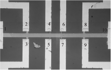
In the Hall-bar geometry (Fig.1) without any magnetic field, in the ohmic regime, with the current applied along the chain axis Sinch11 , we have measured a finite voltage,, across the potential leads. In the normal state between room temperature and , this voltage is weak; its magnitude and sign may depend on the exact current direction with a temperature dependence slightly positive or negative (even nul), as it was checked by injecting the transport current through the two pairs of contact, 2-3 and 8-9, each pair being connected through variable resistors. is also dependent of the sample inhomogeneity. Then, for studying properties of the transverse conduction in the longitudinal CDW sliding state, it is appropriate to have well defined transverse components of the electronic transport. With this respect, we used the pairs of contacts 2-9 or 3-8 as current electrodes. For transverse voltage, , measurements were performed through the opposite potential probes 4-5 and 6-7 . The longitudinal drop of voltage, , was measured on 4-6 or 5-7 contacts. The disturbing voltage signals (thermoelectric etc.) were eliminated by reversing the transport current in the measurements of the temperature dependencies and . Although we measure a transverse voltage, it is more convenient to use resistance rather than voltage in the analysis of the data; then we define and . For studying nonstationary effects a radiofrequency (rf) current was superposed on the dc current using contacts 1 and 10 via two capacitors.
The temperature dependencies and at different currents are shown in Fig.2. The qualitatively same dependencies were observed for the three structures we measured. In the ohmic regime, the dependence at mA (inset in Fig.2 (b)) has the conventional shape for the resistance variation along the conducting chains in NbSe3 in the static pinned state. As can be seen, a qualitatively different dependence takes place for at the same current (inset in Fig.2 (b)). The temperature dependence of does not follow at all the resistance measured at constant current applied along the -axis direction OngBrill but exhibits a sharp drop at and . That indicates moreover a negligible contribution to from the longitudinal voltage variation, which may have resulted possibly due to a misalignment of potential probes or to current injection not strictly parallel to the conducting chains.
The appearance of this electric potential normal to the transport current has been attributed to fluctuations of the critical temperature of the Peierls transition. It has also been demonstrated that the transverse voltage is proportional to the derivative of the longitudinal voltage, (Fig.4 in Ref.Sinch11 ).
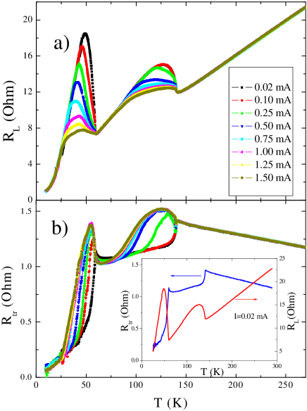
CDWs start to slide for transport current A inducing significant changes in both transverse and longitudinal resistances. As can be seen in Fig.2 (a), maxima of observed below and decrease as usual, indicating the increase of conductivity due to the CDW sliding. The opposite picture is observed in the behaviour (Fig.2 (b)): a strong increase of the transverse voltage takes place below and indicating the decrease of conductivity. As the CDW cannot slide transversely to chains Ayari , the electronic transport in this direction can only be attributed to uncondensed carriers and/or to the conversion CDW - normal carriers.
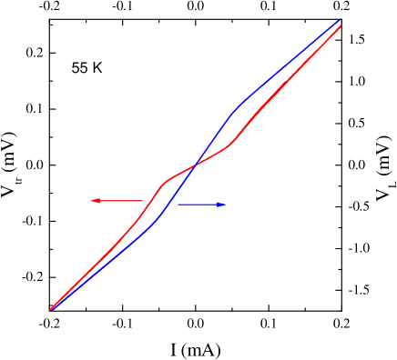
In Fig.3, we have drawn the current-voltage characteristics (IVc) in the transverse (red curve) and the longitudinal (blue curve) directions measured simultaneously for the low temperature CDW ( K). Fig.4 shows the derivatives (red curve) and (blue curve) for the high temperature CDW ( K). The curves for the longitudinal direction are typical IVc: the ohmic behavior is observed at low current and the excess CDW current appears above the threshold current resulting from CDW sliding. For the transverse direction the IVc present the following features:
i) For both CDWs in the vicinity of the threshold current, , defined as the beginning of the decrease of , a sharp increase of is observed. Below this current IVc have a ohmic character.
ii) The increase of (indicated by red dotted lines) occurs at a current which is less than the threshold current for CDW sliding (indicated by blue dotted lines).
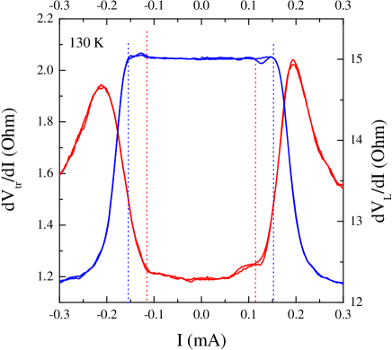
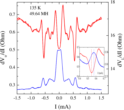
The joint application of dc and rf driving fields leads to appearance of harmonic and subharmonic Shapiro steps in the longitudinal dc IV characteristics Gruner . In the present work we have observed Shapiro steps in both longitudinal and transverse directions below and . Fig.5 shows (red curve) and (blue curve) at 135 K under application of a rf field with a frequency 49.64 MHz. As can be seen, Shapiro steps for longitudinal transport appear in the differential resistance characteristic as spikes, as usual; that corresponds to voltage steps. On the contrary, in the characteristic, minima in the differential resistance are observed, that corresponding to Shapiro current steps. Note that, in our experimental conditions of a low rf power and consequently without complete mode locking, we observe Shapiro steps in transverse transport with a larger amplitude and much more pronounced features when compared to those in the longitudinal direction.
Thus, data indicate that nonlinearity in occurs at a smaller threshold field than in . It has to be noted that the threshold field in elastic measurements, and particularly in the shear compliance data, was also shown to be below that for changes in transport measurements Staresinic01 . Voltage-induced torsional strain is also initiated at voltage below the transport longitudinal threshold, suggesting that the torsional crystal strain is caused by deformations of the CDW, rather than by the CDW current. This torsional strain was attributed to CDW wavefronts being twisted, even without applied voltage and due, for instance to contacts or defects Brill10 .
One may consider the possibility that current density inhomogeneity results from lateral current injection through electrodes 2-9 or 3-8, in the vicinity of which electric field is stronger. Then, depinning may occur near these electrodes at a lower threshold than that between electrodes 4-5 or 6-7. However, we have measured characteristics with current injection from contacts 2-8 and from 1-10 and found a difference less than 2%. In addition, a strong current inhomogeneity which should account for the difference of around 20% between longitudinal and transverse threshold should lead the threshold characteristic to get smeared. In contrast, as seen in Fig. 4, we observe very sharp characteristics longitudinally and transversally with well defined threshold fields. That allows us to conclude that current density inhomogeneity in the measuring part of the sample cannot be the explanation of the effect we are reporting.
The fact that in the transverse direction is less than the longitudinal , but close to it, means that CDW deformations are necessary for CDW sliding. This CDW deformation may be considered as a part of sliding does randomly distributed impurities, being a precursor to sliding. One can also propose the statement in which it is the change in transverse coherence which triggers the longitudinal CDW motion.Thus, when a longitudinal electric field is applied up to , the CDW is deformed up to a certain critical value, above which the transverse CDW coherence is lost. This proposed scenario is in agreement with results of Brazovskii00 ; DiCarlo93 where, from high-resolution x-ray scattering measurements, a strong reduction of the transverse correlation was observed when the CDW moves. Thus, due to the loss of transverse coherence in motion, CDW velocities are distributed along filaments in the -axis.
Due to the presence of impurities in or between chains, a configuration similar to weak links (tunnel contact) between adjacent CDW filaments can be realized. In such a configuration, significant phase shift appears between CDW chains. It was theoretically shown by Artemenko and Volkov Artemenko97 ; ArtemenkoVolkov84 that the transverse current comprises a term proportional to the cosine of the CDW phase difference between neighbouring chains. Let first consider the simple case when the CDW slides with different velocities along two chains coupled by a weak link; then the phases vary with time and alternating tunneling current is generated transversely to the chain direction with a frequency depending on the longitudinal electric field. When an external alternating signal acts on the sample, a resonance will be observed for a fixed if the frequency of the external field and that of the characteristic oscillations coincide. As a result current Shapiro steps will appear in the transverse IV characteristics. This effect shows some analogy with the time-dependent Josephson effect in weakly linked superconductors. However, in a macroscopic sample, the CDW phase fluctuates because the presence of impurities or takes different values in different domains which may wash out the time-dependent phenomena. However, experimentally, we have observed more pronounced features of Shapiro steps in the transverse direction than in the longitudinal one (Fig.5). That may imply a specific synchronisation between oscillations from all the weak links in the sample.
It may have another possible explanation in which the alternating tunneling current takes its origin at the electrodes 4, 5 or 6, 7; at these places the CDW is time dependent along the chain axis but not time dependent in the electrode where the CDW remains pinned , realizing thus a (nearly perfect) junction. However it has to be envisaged that this macroscopic junction (size of 2-3 m) is composed of many microscopic weak links with characteristic dimension of the order of the amplitude CDW coherence length, which is the frame of the theoretical model of Artemenko and Volkov ArtemenkoVolkov84 .
In summary, we have measured for the first time the dynamical properties which occur in the transverse direction to the conducting chains in NbSe3 single-crystals, when the CDW slides along the chains. At an electric field less than the longitudinal threshold one for CDW sliding a sharp decrease in transverse conductivity takes place; that may result from induced phase shifts between CDW chains. Under the joint application of dc and rf driving fields pronounced current Shapiro steps in transverse transport have been observed. The results were tentatively explained in the frame of Artemenko-Volkov theory ArtemenkoVolkov84 ; Artemenko97 . Note that it would be worth to consider the effect of the transverse voltage we have measured in other nonlinear transport CDW phenomena with induced CDW deformations.
Acknowledgements.
The authors are thankful S.A. Brazovskii and especially to S.N. Artemenko for helpful discussions of the experimental results and J. Marcus for help in the sample preparation. The work has been supported by Russian State Fund for the Basic Research (No. 11-02-01379- ), and partially performed in the frame of the CNRS-RAS Associated International Laboratory between CRTBT and IRE ”Physical properties of coherent electronic states in coherent matter”.The support of ANR-07-BLAN-0136 is also acknowledged.References
- (1) G. Grüner, Density Waves in Solids (Addison – Wesley, Reading, Massachusetts, 1994), L. Gor’kov and G. Grüner Charge Density Waves in Solids (Amsterdam: Elsevier Science, 1989), Electronic Crystals 08 edited by S. Brazovskii, P. Monceau and N. Kirova, (Physica B, vol 404, Issues 3-4, 2009).
- (2) V.Ya. Pokrovskii, S.G. Zybtsev, and I.G. Gorlova, Phys. Rev. Lett. 98, (2007) 206404.
- (3) J. Nichols, C.S. Weerasooriya and J.W. Bril, J. Physics: Condens. Matt. 22, (2010) 334224.
- (4) S.N. Artemenko, JETP 84, (1997), 823.
- (5) S.N. Artemenko and A.F. Volkov, Sov. Phys. JETP 60, (1984), 395; JETP Lett., 83, (1983), 368.
- (6) A.A. Sinchenko, P. Monceau and T. Crozes, JETP Lett. 93, (2011), 56.
- (7) N.P. Ong and J.W. Brill, Phys. Rev. B 18, (1978) 5265.
- (8) D. Staresinic, A. Borovac, K. Biljakovic, H. Berger, F. Levy and J.W. Brill, Eur.Phys. J. 24, (2001) 425.
- (9) S. Brazovskii, N. Kirova, H. Requardt, F. Ya. Nad, P. Monceau, R. Currat, J.E. Lorenzo, G. Grübel and Ch. Vettier, Phys. Rev. B 61, (2000) 10640.
- (10) A. Ayari and P. Monceau, Phys. Rev. B 66, (2002) 235119.
- (11) D. DiCarlo, E. Sweetland, M. Sutton, J.D. Brock and R.E. Thorne, Phys. Rev. Lett. 70, (1993) 845.