Electron-photon scattering mediated by localized plasmons: A quantitative analysis by eigen-response theory
Abstract
We show that the scattering interaction between a high energy electron and a photon can be strongly enhanced by different types of localized plasmons in a non-trivial way. The scattering interaction is predicted by an eigen-response theory, numerically verified by finite-difference-time-domain simulation, and experimentally verified by cathodoluminescence spectroscopy. We find that the scattering interaction associated with dark plasmons can be as strong as that of bright plasmons. Such a strong interaction may offer new opportunities to improve single-plasmon detection and high-resolution characterization techniques for high quality plasmonic materials.
pacs:
73.22.-f, 73.20.Mf, 68.49.Jk, 78.67.BfThe strength of the near-field resonant response of plasmonic nanostructures plays an important role in the processes of spontaneous emission Farahani:2005 ; Taminiau:2008 ; Choy:2011 and stimulated emission Berini:2012 ; Bergman:2003 ; Hill:2009 ; Noginov:2009 ; Oulton:2009 . Despite the rapid development of numerical simulation techniques, the strength of resonant response of an arbitrary plasmonic nanostructure is not easy to understand Bigelow:2012 . In particular, the scattering interaction strength between electron and photon mediated by plasmon resonance is non-trivial and, meanwhile, very crucial for high resolution microscopy and spectroscopy on plasmonic nanostructures.
Predicted by an eigen-response theory, dark plasmon modes Stockman:2001 ; Markel:1995 ; Benisty:2009 ) are considered to be weakly-radiative plasmon modes in nanostructures which can give high gain factor in stimulated emission Berini:2012 ; Noginov:2009 . Research interest in dark plasmon modes and the associated Fano phenomena Fano:1961 has been growing rapidly due to many potential applications such as sensors, lasing, and nonlinear and slow-light devices Luk:2010 ; Giannini:2010 ; Zhang:2008 ; Liu:2009 ; Lassiter:2010 ; Fan:2010 . Recently, dark plasmon modes have been observed in optical nanoantennas Schuck:2005 using electronic excitation Abajo:2010 ; Chu:2009 ; Koh:2011 ; Mirsaleh-Kohan:2012 . This opens great opportunity for using electron beam to study the local strength of high quality plasmonic resonances in spatial resolution smaller than 10 nm. In particular, if the dark mode can be observed using cathodoluminescence (CL) spectroscopy Yacobi:1990 , it will show great advantages in imaging plasmonic nanostructures due to its simultaneous high spatial and spectral resolutions.
Here, we use an eigen-response theory Markel:1995 ; Bergman:1980 ; Fung:2007 to study the strong interaction strength of electron-photon scattering mediated by localized plasmons. The theory predicts a counter-intuitive response from dark plasmon, which leads to a strong scattering interaction between a high energy electron and a photon. We use finite-difference-time-domain (FDTD) simulation and CL to verify the theoretical prediction by studying the scattering between electron and photon close to a plasmonic nanoantenna. The theoretical predictions agree with our CL experimental results.
We first briefly introduce the prediction from the eigen-response theory. For a given excitation field , the general response polarization (dipole moment density) can be written as a linear combination of the eigenmodes , where is a label of one eigenmode. In an abstract-vector form, it is written as
| (1) |
where and () are, respectively, the -th eigenmode and the -th eigenvalue of an operator which is defined in the relation between the excitation field and the response through . Since has a dimension of polarizability, it is called eigen-polarizability Fung:2007 of the -th eigenmode. As we will see below, Eq. [1] suggests that a dark mode can contribute to a higher detected signal than a bright mode does in some situations, which seems to be contradictory to our usual believe.
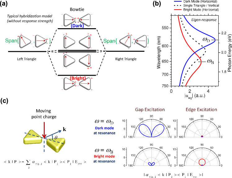
To explain our prediction, let us consider a concrete example (bowtie nanoantenna). Dark modes can be formed in a system of coupled dipole resonators due to the hybridization among dipole modes Markel:1995 , such as in bowtie nanoantenna Schuck:2005 . The hybridization diagram for a bowtie nanoantenna formed by two equilateral Au triangles is shown in Figure 1(a) for the dominant in-plane dipole modes in single triangles. Two-fold degenerate dipole modes in each triangle hybridize with the modes in the opposite triangle, giving a total of four hybridized modes which include horizontal dark and bright modes indicated in Fig. 1(a) and the other almost degenerate vertical modes. The magnitudes of the eigenpolarizbilities, , for these plasmon modes are shown in Fig. 1(b) with their peaks indicating the resonant frequencies. The horizontal dark and bright modes are well-separated in frequency while the vertical modes are almost indistinguishable. In the following, we will focus on distinguishing the horizontal dark and bright plasmon modes. For a system that supports one dark mode and one bright mode , the radiation amplitude (i.e., the interaction strength with free photon) is
| (2) |
In general, has a magnitude smaller than (see Fig. 1. However, a dark mode with high quality factor should also have larger magnitude of at resonance Fung:2008 ). As a result, the magnitude of can be comparable with . In addition, a crucial factor that determines the ultimate radiation is the projection magnitudes and . By choosing a zero projection to the bright mode (i.e., making , we can have strong photon radiation dominated by the dark mode, which means a strongly enhanced interaction between electron and photon by dark plasmon. Details of how each of these quantities contributes to the strong interaction are illustrated in the Supplemental Material. For an excitation by a high energy electron (30 keV), the final interaction strength predicted by the theory is shown in Fig. 1(c).
To support our prediction, we performed FDTD simulations as well as experiments for the case of excitation by electron beam, which is considered to be a fine and controllable excitation source. In both our simulation and experiment, a 30 keV electron beam is incident normally to a bowtie nanoantenna. Electron beam is modeled in FDTD simulation as a moving point charge. Details of simulation method can be found in Supplemental Material and elsewhere Chaturvedi:2009 . The three dimensional geometry of the bowtie antenna in our simulation is almost the same as in the experiment, except the imperfection of the fabricated sample and the very thin (3nm) adhesion layer below Au particles. To match the fabricated sample, all corner and edges in the model structure have a rounding radius of 15 nm.
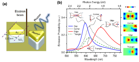
Fig. 2(a) shows a schematic of the problem we consider. We simulate and measure the photon emission for different fixed e-beam locations, which indicates the strength of the scattering interaction between electron beam and photon. Simulation results in Fig. 2(b) show that there is a dominant peak associated with each fixed e-beam. When the e-beam is fixed at the center (gap), right upper corner, and right edge of the bowtie antenna, we observe a peak at 600 nm, 620 nm, and 680 nm, respectively. We see that there are at least three different plasmon modes supported by the bowtie antenna. This is consistent with our prediction that four resonant modes are supported while two of the modes are almost degenerate such that they can hardly be distinguished. To further verify our theory and understand the peaks, we also simulate the case of single nanotriangle [dashed line in Fig. 2(b)]. Such a peak wavelength corresponds to the dipole resonance of single nanotriangle while the peaks for gap, edge, and corner excitations correspond to anti-parallel horizontal dipoles, parallel horizontal dipoles, and vertical dipoles, respectively. The above classification of peaks is verified by simulating the field patterns at the corresponding peaks in Fig. 2(b). The right colored panels in Fig. 2 show the z-component of the electric field at a plane located 2 nm above the surface of the bowtie nanoantenna for the three dominant peaks. These patterns can approximately represent the surface charge density. We see that, when fixing e-beam at the central gap and observing the field pattern at the wavelength of 600 nm, the distribution of the induced charges is symmetric in y-direction, which represents a pair of anti-parallel dipoles. For edge excitation at 680 nm, the induced charges show an almost antisymmetric distribution except the field produced by the e-beam itself near the right edge. For corner excitation at 620 nm, the induced charges show a pair of anti-parallel vertical dipoles. This agrees with our theory that the vertical modes have wavelengths very close to the single triangle case. Apart from the dominant peak positions, we also see some small features at shorter wavelengths, which may corresponds to higher order modes.
Here, we briefly discuss why both dark and bright modes can be selectively excited and analyzed in the far-field with strong signals. When we fix the e-beam at the center of the gap, the excitation field produced by the e-beam has an azimuthal symmetry with respect to the center of the bowtie. Therefore, only the plasmon with charge distribution symmetric in both directions can be excited ( and ) and this leads to a pure excitation of horizontal anti-parallel dipole mode, which has the shortest wavelength among the three observable peaks. When the e-beam is fixed at the edge, a mirror symmetry is broken and the excitation of the horizontal parallel dipole mode is possible ( and ). Since the e-beam is far away from the center of bowtie nanoantenna, it is more favorable to the excitation of horizontal parallel mode, which leads to a peak at the longest wavelength. Similarly, in the case of e-beam fixed at the corner, the vertical dipole modes can be excited due to the broken mirror symmetry in the vertical direction. Details of the projection magnitudes and the emission strengths as a function of the position of electron beam are described in the Supplemental Material.
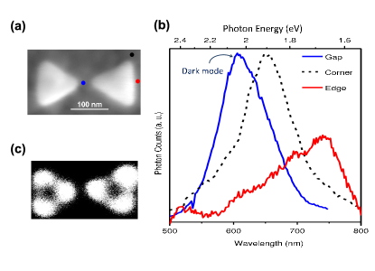
The gold bowtie nanoantenna was fabricated using electron-beam lithography on a multilayered substrate with minimal background luminescence and relatively low substrate index Kumar:2010 . In our CL experiment, an Aluminum parabolic mirror, with a small hole for electron beam, was placed on top of the sample collected the photons emitted by the antenna irradiated with an electron beam accelerated at 30 kV and 20 nA current. The collected photons were directed into a Mach-Czerny type monochromator to collect spectral information and imaging. Experimental setup have been previously published with details Chaturvedi:2009 ; Kumar:2010 . More information related to this experiment is included in Supplemental Material. Our experimental results (Fig. 3) show the strong scattering interaction mediated by the dark plasmon, which agrees very much with our theory. An SEM picture of the fabricated bowtie nanoantenna is shown in Fig. 3(a). We observed three peaks for center (gap), corner, and edge excitations, indicated in the same SEM picture as blue, black, and red dots, respectively. The observation of the three modes is consistent with a previous related experiment Koh:2011 . The results [Fig. 3(b)] also agree well with the simulation results in terms of the number of peaks and relative peak positions, except the separation between peaks are larger in the experiment. The obtained peak wavelengths for center, corner, and edge excitations are, respectively, 600 nm, 650 nm, and 740 nm. We believe that the discrepancy from simulation results can be due to the detailed material and geometrical properties. The panchromatic CL image [Fig. 3(c)] also indicates that the edge excitation gives a weak signal even the bright mode is excited.
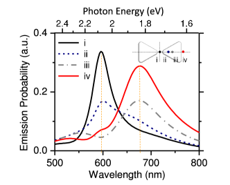
To further demonstrate the roles of projected magnitudes , we repeat the simulation by changing the position of the electron beam from the gap to the edge. The results in Fig. 4 show the peak positions for different e-beam excitation locations are the same except the strength of signal, indicating a gradual change in projection magnitude from domination of anti-parallel mode to parallel mode (from “i” to “iv”). We see that there is no component of parallel mode contributing to the response when the e-beam is located at the gap and the radiation from the anti-parallel mode is thus the only dominant mode observed. It should be emphasized that the signal for position “i” is even higher than that of the parallel mode for position “iv”, indicating a strong interaction between electron beam and photon. This is also observed in our experimental results in Fig. 3(b).
To conclude, we introduced a nontrivially strong electron-photon scattering interaction enhanced by dark plasmon modes. Our theory predicts that even though dark plasmon mode couples weakly with photon, it can strongly enhance the scattering interaction between a high energy electron and a photon. Our simulation and experiment strongly support the theoretical predictions. The discovery may offer new opportunities for improving single-plasmon generation and detection in nanostructures. Our study also provides new insights for developing new high-resolution characterization techniques for high quality plasmonic materials. The phenomenon presented in this Letter is explained by a classical model. It would be interesting to study the quantum interaction in the future.
This work was supported by National Science Foundation and the Office of Naval Research and carried out in part in the Frederick Seitz Materials Research Laboratory Central Facilities, University of Illinois, which are partially supported by the U.S. Department of Energy. We thank Dr. Jun Xu, Dr. Hyungjin Ma, Prof. C. T. Chan, Prof. Lei Zhou, and Prof. Min Chen for fruitful discussions.
I References
References
- (1) J.N. Farahani, D.W. Pohl, H.J. Eisler, B. Hecht, Phys. Rev. Lett. 95, 017402 (2005).
- (2) T.H. Taminiau, F.D. Stefani, F.B. Segerink, N.F. van Hulst, Nat. Photon. 2, 234–237 (2008).
- (3) J.T. Choy, B.J.M. Hausmann, T.M. Babinec, I. Bulu, M. Khan, P. Maletinsky, A. Yacoby, M. Lon ar, Nature Photon. 5, 738–743 (2011).
- (4) P. Berini, I. De Leon, Nature Photon 6, 16–24 (2012).
- (5) D.J. Bergman, M.I. Stockman, Phys. Rev. Lett. 90, 027402 (2003).
- (6) M.T. Hill et al., Opt. Express 17, 11107–11112 (2009).
- (7) M.A. Noginov, G. Zhu, A.M. Belgrave, R. Bakker, V.M. Shalaev, E.E. Narimanov, S. Stout, E. Herz, T. Suteewong, U. Wiesner, Nature 460, 1110–1113 (2009).
- (8) R.F. Oulton, V.J. Sorger, T. Zentgraf, R.M. Ma, C. Gladden, L. Dai, G. Bartal, X. Zhang, Nature 461, 629–632 (2009).
- (9) N.W. Bigelow, A. Vaschillo, V. Iberi, J.P. Camden, and D.J. Masiello, ACS Nano 6, 7497–7504 (2012).
- (10) M.I. Stockman, S.V. Faleev, D.J. Bergman, Phys. Rev. Lett. 87, 167401 (2001).
- (11) V.A. Markel, J. Opt. Soc. Am. B 12, 1783–1791 (1995).
- (12) H. Benisty, J. Opt. Soc. Am. B 26, 718–724 (2009).
- (13) U. Fano, Phys Rev 124, 1866–1878 (1961).
- (14) B. Luk’yanchuk, N.I. Zheludev, S.A. Maier, N.J. Halas, P. Nordlander, H. Giessen, C.T. Chong, Nature Mater 9, 707–715 (2010).
- (15) V. Giannini, A.I. Fernández-Domínguez, Y. Sonnefraud, T. Roschuk, R. Fernández-García, S.A. Maier, Small 6, 2498–2507 (2010).
- (16) S. Zhang, D.A. Genov, Y. Wang, M. Liu, X. Zhang, Phys. Rev. Lett. 101, 047401 (2008).
- (17) N. Liu, L. Langguth, T. Weiss, J. Kästel, M. Fleischhauer, T. Pfau, H. Giessen, Nature Mater. 8, 758–762 (2009).
- (18) J.B. Lassiter, H. Sobhani, J.A. Fan, J. Kundu, F. Capasso, P. Nordlander, N.J. Halas, Nano Lett. 10, 3184–3189 (2010).
- (19) J.A. Fan, K. Bao, C.H. Wu, J.M. Bao, R. Bardhan, N.J. Halas, V.N. Manoharan, G. Shvets, P. Nordlander, F. Capasso, Nano Lett. 10, 4680–4680 (2010).
- (20) P.J. Schuck, D.P. Fromm, A. Sundaramurthy, G.S. Kino, W.E. Moerner, Phys. Rev. Lett. 94, 017402 (2005).
- (21) F.J.G. de Abajo, Rev. Mod. Phys. 82, 209–275 (2010).
- (22) M.W. Chu, V. Myroshnychenko, C.H. Chen, J.P. Deng, C.Y. Mouand, F.J.G. de Abajo, Nano Lett. 9, 399–404 (2009).
- (23) A.L. Koh, A.I. Fernández-Domínguez, D.W. McComb, S.A. Maier, J.K.W. Yang, Nano Lett. 11, 1323–1330 (2011).
- (24) N. Mirsaleh-Kohan et al., J. Phys. Chem. Lett. 3, 2303–2309 (2012).
- (25) B.G. Yacobi, D.B. Holt, Cathodoluminescence Microscopy of Inorganic Solids (Plenum, New York, 1990).
- (26) D.J. Bergman, D. Stroud, Phys. Rev. B 22, 3527–3539 (1980).
- (27) K.H. Fung, C.T. Chan, Opt. Lett. 32, 973–975 (2007).
- (28) K.H. Fung, C.T. Chan, Phys. Rev. B 77, 205423 (2008).
- (29) P. Chaturvedi, K.H. Hsu, A. Kumar, K.H. Fung, J.C. Mabon, N.X. Fang, ACS Nano 3, 2965–2974 (2009).
- (30) A. Kumar, K.H. Fung, J.C. Mabon, E. Chow, N.X. Fang, J. Vac. Sci. Technol. B 28, C6C21–C6C25 (2010).