1
High Van Hove singularity extension and Fermi velocity increase in epitaxial graphene functionalized by gold clusters intercalation
Abstract
Gold intercalation between the buffer layer and a graphene monolayer of epitaxial graphene on SiC(0001) leads to the formation of quasi free standing small aggregates of clusters. Angle Resolved Photoemission Spectroscopy measurements reveal that these clusters preserve the linear dispersion of the graphene quasiparticles and surprisingly increase their Fermi velocity. They also strongly modify the band structure of graphene around the Van Hove singularities (VHs) by a strong extension without charge transfer. This result gives a new insight on the role of the intercalant in the renormalization of the bare electronic band structure of graphene usually observed in Graphite and Graphene Intercalation Compounds.
pacs:
68.65.-k, 81.16.Fg, 81.07.-b, 81.16.Rf, 82.30.RS, 82.65.+rThe enormous craze for graphene is due to the coexistence between
the fundamental aspects of research and the increasing number of
potential applications. From the fundamental point of view, this
system brings together the physics of particles with relativistic
behaviors and the condensed matter. It becomes a promising
material for the next generation of nanoelectronic devices
destined to supplant silicon NovoselovNature2005 . However
the main drawback limiting the potential use of graphene stems
from its intrinsic characteristics: a semiconductor with zero gap,
almost inert towards controlled chemisorption and doping. One of
the main challenges is to functionalize the graphene layer while
preserving its fascinating properties. Different ways of
functionalization have been opened. Deposition of metal or
molecules on top of graphene could allow to modify the Fermi level
or to induce long range superconductive correlations (for example
using superconducting metal contact)
BouchiatPRL2010 ; DirksNatPhysics2011 . It is also possible to
intercalate metal clusters or molecules between the graphene
layers, opening the possibility to functionalize the graphene
layer on both sides creating a Graphene-Based Hybrid structure
(GBHs). In the latter case, the potentialities of modification of
the graphene band structure by intercalation meet the historical
research community of the Graphite Intercalation Compounds (GICs),
well-known in the community of Carbon and also for its famous
application which is the Li-ion battery. The research in this
field has been considerably intensified after the recent discovery
of high Tc superconductivity for the GIC
WellerNatPhys2005 . Despite this intense activity, it is
still not yet clear if the superconductivity is due to the nature
of the intercalant or to the graphene plane itself. Angle Resolved
Photoemission Spectroscopy (ARPES) measurements have revealed a
systematic VHs extension for these graphitic superconductor
VallaPRL2011 . Moreover, recently, in the case of
the superconducting property has been associated to Charge Density
Waves (CDW) evidenced by STM EllerbyNature2011 . In this
context, epitaxial graphene consists of a playground to understand
how the band structure of graphene could be modified and more
particularly the various many-body phases that we could expect
near VHs. Indeed, the growth of graphene monolayer on silicon face
of silicon carbide substrate leads to the formation of a monolayer
graphene covalently bonded to the substrate (called buffer layer)
which decouples the true monolayer graphene in weak interaction
with it. An intercalation process is then possible between these
two layers. As the transition from the monolayer to bilayer and
few layers graphene can be done in a controlled way on SiC(0001),
this system is also particularly interesting to follow the
staging sequences of the intercalation process. In a detailed
study by Scanning Tunneling Microscopy (STM), we have revealed
that upon specific preparation procedure gold intercalates in two
different structures PremlalAPL09 . One is the formation of
small intercalated clusters. We have shown by STM that these
intercalated gold clusters create a strong ”standing waves-like”
pattern, on the upper monolayer graphene which has been attributed
to a possible VHs singularity extension cranneyEPL10 .
The goal of the present work was to realize homogeneous surfaces with intercalated gold clusters
and to explore the band structure of this functionalized graphene
on the occupied states with ARPES measurements. We report here
ARPES and STM studies of pristine epitaxial graphene and
with the intercalation of gold clusters.
The graphene samples were prepared in UHV by the annealing of n-doped SiC(0001) at 900 K for several hours and subsequent annealing at 1500 K VanBommelSurfSci75 ; SimonPRB99 ; others . The deposition of gold on graphene was carried out at room temperature using a homemade Knudsen cell calibrated using a Quartz Crystal Microbalance. The sample was further annealed at 1000 K for 5 min PremlalAPL09 . In order to avoid frequent confusion, we would like to notice that the literature reports two types of intercalation process. One occurs during the annealing process of the carbon rich SiC(0001) reconstruction in presence of a foreign element for example H, F or Au BostwickScience2010 ; WalterAPL2011 ; GierzPRB2010 ; StarkePRB11 ; WongACSNano11 . This leads to the intercalation between the SiC substrate and the C-rich initially covalently bonded graphene layer leading to a partial decoupling. This is associated to a p-type doping effect. In our case the deposition of gold is done after the complete realization of the graphene monolayer leading to the intercalation between the top graphene layer and the buffer layer. Our STM experiments were performed with a LT-STM from Omicron at 77 K at a base pressure in the mbar range. The images were acquired using a lock-in amplifier and a modulation voltage of . The ARPES measurements were carried out on the CASSIOPEE beamline of the SOLEIL synchrotron radiation source using a Scienta R4000 electron spectrometer. The spectra were recorded at a photon energy of 60 eV with an overall energy resolution of around 30 meV at a temperature of 10 K. All the samples were prepared in a separated UHV system and then characterized by STM. They were then transported in air prior to their introduction in the UHV system of the synchrotron radiation source. A soft degassing process at 500K was performed during several minutes prior to measurements.
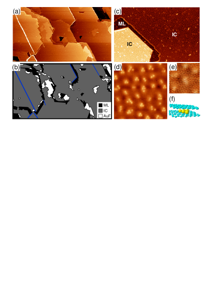
Figure 1 shows the resulting STM images of the epitaxial
graphene monolayer with the deposition of gold atoms followed by
annealing process as previously described. ARPES measurements
require surfaces as homogeneous as possible, which has been done
here. We are able to control the deposition and annealing process
in order to obtain a fairly homogeneous surface with the given
intercalation process. Indeed figures 1a) and b) show
respectively a large scale STM image of the studied sample and the
corresponding scheme of the repartition of the different domains
obtained. More than 80% of the surface is covered with the
intercalated gold clusters (IC) . A small part is occupied by
pristine monolayer (ML) and by another domain which corresponds to
the insertion of a continuous monolayer of gold (AuF). The
continuous monolayer of gold has been evidenced by a Moiré
pattern and is associated to a p-doping effect
PremlalAPL09 . The bright lines in a) correspond to the
initial puckers currently observed on the pristine ML graphene,
that are known to be due to the cooling process after the
annealing. These defects play probably a role in the intercalation
of metal as they are systematically observed on the border of
areas with intercalated gold. As shown in figures c) and d), the
gold clusters are evidenced by bright protrusion visible at high
negative bias (probing the full states). The intercalated gold
atoms on the IC domains form a quasi periodically arrangement of
aggregates of clusters intercalated between the buffer layer and
the top graphene monolayer. Indeed in e) a high resolution image
performed at low bias (-100 meV) shows the graphene plane over
gold clusters where the 6 carbon atoms of the honeycomb structure
are equally visible. This definitively proves that gold clusters
are just under the top graphene monolayer. These clusters are less
visible for the low bias voltage and the honeycomb structure of
graphene dominates the contrast. In Figure d), we tentatively
attributed these bright spots to aggregates of flat clusters made
of 6 atoms as schematized in figure f) PremlalAPL09 . This
proposed model is however still under debate and currently tested
by DFT calculations, but the discussion of the exact nature of
these
clusters is out of the scope of this article.
We have shown that these clusters create standing waves patterns
for bias voltage corresponding to the unoccupied states starting
from +0.6 to +1 eV
cranneyEPL10 . The non-dispersive character of these
standing waves let us consider them as charge density waves (CDW).
We have attributed these structures as a screening effect. Indeed
we know that in the epitaxial graphene the top Graphene ML is
n-doped due to the transfer of charges from the substrate. The Au
clusters seem to screen these charges which create a charge
inhomogeneity on the graphene plane and scatter the QPs. We have
used the Fourier Transform Scanning Tunnelling Spectroscopy
Technique (FT-STS) JofCondMater07 i. e. we performed a 2D
FT of the dI/dV map images with standing waves pattern in function
of the bias voltage. This technique was already successfully used
in order to determine the full band structure dispersion of the 2D
system VonauPRL05 ; JPhysD2011 . Here the FT-STS
showed elliptic features around M points which have been
attributed to a fingerprint of large extension of the VHs. As
these results were obtained on the empty states in the band
structure, we wanted to explore the filled states with ARPES
measurements. In the case of the epitaxied graphene ML on
SiC(0001), the graphene dispersion band is not contaminated by
the bulk band structure for a large scale of energy and up to the expected VHs VarchonPRL2007 .
The experimental spectral functions of our epitaxial ML graphene samples, without and with intercalated gold clusters are shown respectively in figures 2 b) and c). Both samples exhibit the characteristic linear dispersion around the K point. The Dirac point is at 230 meV below the Fermi level for the functionalized graphene with gold clusters and 260 meV for the pristine graphene. The doping due to the clusters is quite negligible as previously deduced from STS measurements PremlalAPL09 . For the pristine ML graphene (Fig. 2b), we obtain a very good dispersion characterized by thin bands and linearity over nearly . The dispersion band indicates that the pristine ML graphene is of very high quality. In the case of graphene with intercalated gold clusters (Fig.2c) the bands are much broader. This is probably due to the reduced size of the homogeneous domains. However the dispersion is also linear until -2 eV . The band exhibits a strong ”kink” when approaching the VHs below -2 eV.
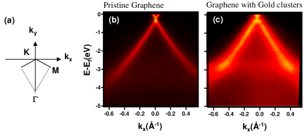
This is associated to a high
increase in the spectral intensity. This is the characteristic of
a strong renormalization of the band structure which is usually
due to a doping dependence with electron-electron correlation,
electron-phonon coupling or electron-plasmon coupling. The
surprise here comes from the Fermi velocity of the quasiparticles.
For the pristine graphene we deduced from the slope a group
velocity of while is measured in the case of the
functionalized graphene with gold. Although the uncertainty is
larger in the latter case, this Fermi velocity is increased by
more than 20% of the initial value.
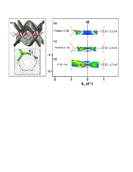
The constant energy
surfaces around the M points give also remarkable results. The
figure 3a) recalls the band structure and the interesting
topological points of graphene with the calculated Constant Energy
Contours (CEC). In b), c) and d) we present respectively the
constant energy maps around the M point (which is the position of
the expected VHs) at different energies. The VHs are found at -2.8
eV in the case of pristine graphene in figure 3c) and at -2.3 eV
in the case of graphene with gold in fig. 3 d). As shown
in 3b) the VHs is not reached at -2.3 eV without the presence of
gold clusters. The isocontour in d) (with gold) is strongly warped
and the apex of the triangular shaped contour is filled
approaching the VHs. These results confirm our interpretation of
standing waves pattern and features observed in FT-STS attributed
to a large VHs extension cranneyEPL10 . The reason of such a
VHs extension remains an open question for the moment. It seems
that there is a general behavior of the graphene band structure in
the case of intercalated compounds (graphite and epitaxial
graphene) particularly around the VHs. Indeed, similar results
have been obtained on epitaxial graphene where strong VHs
extension has been observed after the intercalation of K and Ca in
epitaxial graphene layer McChesneyPRL2010 . In this latest
experiment the graphene was strongly n-doped and the Fermi level
was positioned at the VHs of the graphene-derived states
which are usually suspected to be at the origin of the
superconductivity. Up to now, whatever the studied system (GICs or
intercalated graphene), the intercalant was considered to be
homogeneously distributed between graphene planes leading to
specific surstructures (usually a p-2x2) depending on the
stoichiometryDresselhauss2002 . However in each of these
cases the VHs extension has been associated to a highly doping
process and electron-electron correlation. The Fermi velocities
were found generally lower (0.5 to ).
In our case the electron-electron correlation has to be ruled out.
The sample is no more doped compared to the pristine graphene and
the Fermi velocity is increased by the intercalated clusters. The
Fermi velocities, we have measured for Pristine graphene and with
intercalated gold clusters are comparable to those found in the
literature, i. e. to for
epitaxial graphene on SiC for the Si terminated face and
for the carbon terminated face (see
for example SeyllerPSS2008 ), or
in the case of exfoliated
graphene on NovoselovNature2005 . Then the Fermi
velocity we have measured with the intercalated gold clusters is
comparable to the one measured on graphene epitaxied on the
C-face. This tends to demonstrate that the clusters decouple the
graphene layer from the substrate as in the case of C- face
graphene layers. However this leads to a counterintuitive
reasoning. Indeed, among the all possible origins of the VHs
extension, the pseudo periodic potential created by the clusters
is the most probable hypothesis.
Following the theoretical calculation of Cheol et al.
LouieNature2008 , applying a weak pseudopotential should
leads to decrease the group velocity (renormalization). This work
also shows that a slight potential oscillation and/or corrugation
on the graphene layer tends to strongly modify the VHs. Here the
compressive strain of graphene is probably partially released by
the decoupling induced by the clusters, leading to an increase of
lattice parameter and consequently an increase of the Fermi
velocity compared to pristine graphene. Concerning the VHs
extension, one more time this appears to be a general
characteristic of the graphene electronic properties. Indeed, as
soon as the hopping process of the quasiparticule is modified,
either theoretically by the modification of the Hopping potential
BenaPRB11 or experimentally by the modification of the
rotation angle between two graphene layers
AndreiNatPhys2010 , the VHs are affected. In a very complete
detailed study of the graphitic superconductors, it has been
demonstrated that critical temperature Tc depends on the charge
transfer between the intercalated atoms and the graphene plane
i.e. the doping level. The increase of Tc was correlated to an
expected electron-phonon coupling which is associated to the kink
in the dispersion band structure VallaPRL2011 . This was
also associated to a strong anisotropic Fermi velocity and
trigonal warping in the constant energy contour map around the K
point approaching the Fermi level. The reason why these clusters
modify the band structure in this way remains an open question but
in this context, considering the importance of the controversial
possible role of the VHs in the superconductivity property (VHs
extension scenario), particularly in the case of GICs, our results
open a new way for the understanding of this phenomena. Indeed
here the graphene is not strongly doped, and the intercalant is
not homogeneously distributed. The last but not the least point of
this study is to show one more time the link between the FT-STS
and ARPES measurements, even if it is not discussed in detail
cranneyEPL10 .
Acknowledgements.
This work is supported by the Région Alsace and the CNRS. The Agence Nationale de la Recherche supports this work under the ANR Blanc program, reference ANR-2010-BLAN-1017-ChimiGraphNReferences
- (1) K. S. Novoselov, A. K. Geim, S. V. Morozov, D. Jiang, M. I. Katsnelson, I. V. Grigorieva, S. V. Dubonos, and A. A. Firsov, Nature 438, 197 (2005).
- (2) B. M. Kessler, C .Ö. Girit, A. Zettl, and V. Bouchiat, Phys. Rev. Lett. 104, 047001 (2010).
- (3) Travis Dirks, Taylor L. Hughes, Siddhartha Lal, Bruno Uchoa, Yung-Fu Chen, Cesar Chialvo, Paul M. Goldbart, and Nadya Mason, Nat. Phys. 7, 386 (2011).
- (4) T. Weller, M. Ellerby, S. Saxena, R. Smith, and N. Skipper, Nat. Phys. 1, 39 (2005).
- (5) Z.-H. Pan, J. Camacho, M. H. Upton, A. V. Fedorov, C. A. Howard, M. Ellerby, and T. Valla, Phys. Rev. Lett. 106, 187002 (2011).
- (6) K.C. Rahnejat, C.A. Howard, N.E. Shuttleworth, S.R. Schofield, K. Iwaya, C.F. Hirjibehedin, Ch. Renner, G. Aeppli, and M. Ellerby, Nat. Commun. 2:558 doi: 10.1038/ncomms1574 (2011).
- (7) B.Premlal et al., Appl. Phys. Lett. 94, 263115 (2009).
- (8) M. Cranney, F. Vonau, P.B. Pillai, E. Denys, D. Aubel, M.M. De Souza, C. Bena, and L. Simon, EPL 91, 66004 (2010).
- (9) A. J. Van Bommel et al, Surf.Sci. 48, 463(1975).
- (10) L. Simon, J. L. Bischoff, and L. Kubler, Phys. Rev. B 60, 11653 (1999).
- (11) C. Berger, Z. Song, T. Li, X. Li, A. Y. Ogbazghi, R. Feng, Z. Dai, A. N. Marchenkov, E. H. Conrad, P. N. First, and W. A. de Heer, J. Phys. Chem., 108, 19912 (2004).
- (12) A. Bostwick, F. Speck, T. Seyller, K. Horn, M. Polini, R. Asgari,A. H. MacDonald, and E. Rotenberg, Science 328, 999 (2010).
- (13) A. L. Walter, K.-J Jeon, A. Bostwick, F. Speck, M. Ostler, T. Seyller, L. Moreschini, Y. S. Kim, Y. J. Chang, K. Horn, and E. Rotenberg, Appl. Phys. Lett. 98, 184102 (2011).
- (14) I. Gierz, T. Suzuki, R. T. Weitz, D. S. Lee, B. Krauss, C. Riedl, U. Starke, H. Höchst, J. H. Smet, C. R. Ast, and K. Kern, Phys. Rev. B 81, 235408 (2010).
- (15) S. Forti, K. V. Emtsev, C. Coletti, A. A. Zakharov, C. Riedl, and U. Starke, Phys. Rev. B 84, 125449 (2011)
- (16) Swee Liang Wong, Han Huang, Yuzhan Wang, Liang Cao, Dongchen Qi, Iman Santoso, Wei Chen and Andrew Thye Shen Wee, ACSNANO 5, 7662 (2011).
- (17) L. Simon, F. Vonau and D. Aubel, J. of Phys. Cond. Mat., 19, 355009 (2007).
- (18) F. Vonau, D. Aubel, G. Gewinner, S. Zabrocki, J. C. Peruchetti, D. Bolmont, and L. Simon, Phys. Rev. Lett. 95, 176803 (2005).
- (19) L. Simon, C. Bena, F. Vonau, M. Cranney and D. Aubel, J. Phys. D 44, 464010 (2011).
- (20) F. Varchon, R. Feng, J. Hass, X. Li, B. Ngoc Nguyen, C. Naud, P. Mallet, J.-Y. Veuillen, C. Berger, E. H. Conrad, and L. Magaud, Phys. Rev. Lett. 99, 126805 (2007).
- (21) Jessica L. McChesney, Aaron Bostwick, Taisuke Ohta, Konstantin V. Emtsev, Thomas Seyller, Karsten Horn, and Eli Rotenberg, Phys. Rev. Lett. 104, 136803 (2010).
- (22) M.S. Dresselhaus, and G. Dresselhaus Advances in Physics vol 51, p1-186 (2002).
- (23) I. Horcas et al, Rev. Sci. Instrum. 78, 013705 (2007).
- (24) Th. Seyller, A. Bostwick, K. V. Emtsev, K. Horn, L. Ley, J. L. McChesney, T. Ohta, J. D. Riley, E. Rotenberg, and F. Speck Phys. Stat. Sol. (b) 245, 1436 (2008).
- (25) Cheol-Hwan Park, Li Yang, Young-Woo Son, Marvin L. Cohen and Steven G. Louie Nat. Phys. 4, 213 (2008).
- (26) Cristina Bena, and Laurent Simon, Phys. Rev. B 83, 115404 (2011).
- (27) Guohong Li, A. Luican, J. M. B. Lopes dos Santos, A. H. Castro Neto, A. Reina, J. Kong, and E. Y. Andrei, Nat. Phys. 6, 109 (2010).