Spectroscopy of spin-orbit quantum bits in indium antimonide nanowires
Abstract
Double quantum dot in the few-electron regime is achieved using local gating in an InSb nanowire. The spectrum of two-electron eigenstates is investigated using electric dipole spin resonance. Singlet-triplet level repulsion caused by spin-orbit interaction is observed. The size and the anisotropy of singlet-triplet repulsion are used to determine the magnitude and the orientation of the spin-orbit effective field in an InSb nanowire double dot. The obtained results are confirmed using spin blockade leakage current anisotropy and transport spectroscopy of individual quantum dots.
pacs:
73.63.Kv, 85.35.BeThe spin-orbit interaction (SOI) describes coupling between the motion of an electron and its spin. In one dimension, where electrons can move only to the left or to the right, the SOI couples this left or right motion to either spin-up or spin-down. An extreme situation occurs in what is called a helical liquid Streda2003 where, in the presence of magnetic field, all spin-up electrons move to the left and all spin-down electrons to the right. As proposed recently Lutchyn2010 ; Oreg2010 , a helical liquid in proximity to a superconductor can generate Majorana fermions Kitaev2001 . The search for Majorana fermions in 1D conductors is focused on finding the best material in terms of a strong spin-orbit interaction and large Landé g-factors. The latter is required for a helical liquid to exist at magnetic fields that do not suppress superconductivity. High g-factors of the order 50, strong SOI and the ability to induce superconductivity put forward InSb nanowires Nilsson2009 ; Nilsson2011 as a natural platform for the realization of 1D topological states.
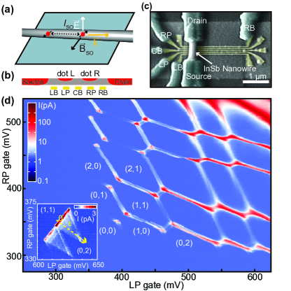
The SOI can be expressed as an effective magnetic field that depends on the electron momentum. An electron moving through the wire undergoes spin precession around with a rotation over a distance lSO called the spin-orbit length (see Fig. 1(a)). The length lSO is a direct measure of the SOI strength: a stronger SOI results in a shorter lSO. In this letter, we use spin spectra of single electrons in quantum dots Schreiber2010 to extract lSO and the direction of . In quantum dots, the SOI hybridizes states with different spin Nilsson2009 ; Pfund2007a ; Fasth2007 . For a single electron, the SOI-hybridized spin-up and spin-down states form a spin-orbit qubit Nadj-Perge2010a ; Nowack2007 . For two electrons SOI hybridization induces level repulsion between singlet and triplet states. The resulting level-repulsion gap between the well-defined qubit states can be used to measure the SOI: the gap size is determined by lSO Nilsson2009 ; Pfund2007a ; Fasth2007 and the gap anisotropy indicates the direction of Takahashi2010PRL ; KanaiY2011 ; Golovach2008 .
Double quantum dots in InSb nanowires are defined by local gating (Figs. 1(b),1(c)). A finite voltage is applied across the source and drain electrodes; and the current through the nanowire is measured. Five gates underneath the wire create the confinement potential and control the electron number on the two dots Fasth2007 ; Nadj-Perge2010 . We focus on the (1,1) charge configuration (Fig. 1(d)), in which both the left and the right dot contain exactly one electron, each of them representing a qubit Nadj-Perge2010a ; Nowack2007 ; Pioro-Ladriere2008 ; Petta2005a ; Koppens2006 .

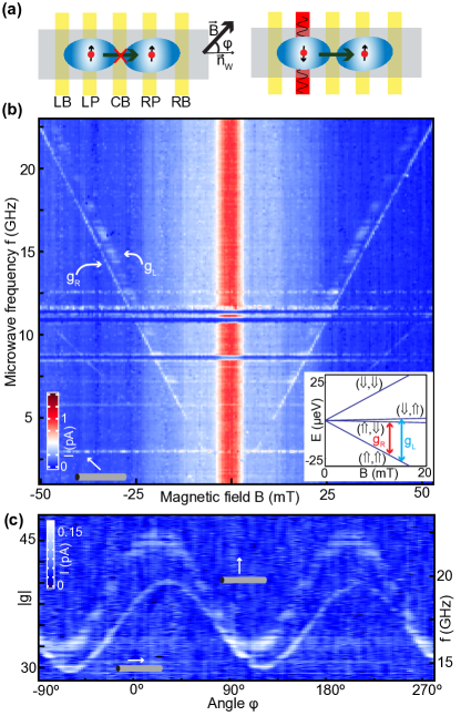
The qubit eigenstates are described by the Kramers spin-orbit doublet and . These two states are superpositions of spin-up and spin-down, and of several of the lowest orbital states Flindt2006 . Similar to the case of pure spin states, a magnetic field B induces a Zeeman splitting EZ = gBB between the Kramers doublets, where g is the effective Landé g-factor for a given direction of , and is the Bohr magneton. The two qubits in the (1,1) configuration can either form a Kramers singlet state S(1,1) or one of the three triplets T+(1,1), T0(1,1) and T-(1,1). The states of the qubits are prepared using Pauli spin blockade Nadj-Perge2010a ; Nowack2007 ; Petta2005a ; Koppens2006 ; Ono2002a (Fig. 2(a)), which relies on the tunneling process from (1,1) to the (0,2) spin singlet S(0,2) (note that T(0,2) state is at 5 meV above S(0,2) and therefore inaccessible for B = 0). When the two electrons form a triplet state, tunneling of the left electron to the right dot is prohibited by selection rules. This absence of tunneling initializes the qubits in the so-called blocked (1,1) state and thereby suppresses the current of electrons passing through the double dot. Leakage current can occur due to hybridization of T(1,1) states with S(0,2) induced by SOI and by spin mixing between T(1,1) and S(1,1) due to hyperfine interaction Nadj-Perge2010 ; Koppens2005 ; Pfund2007a ; Danon2009a .

Transitions between qubit states are induced by a.c. electric fields via electric dipole spin resonance (EDSR) Nadj-Perge2010a ; Nowack2007 ; Pioro-Ladriere2008 ; Bell1962 ; Golovach2006 ; Laird2007 . Voltages at microwave frequencies are applied to the left plunger (LP) gate (Fig. 2(a)). The oscillating electric field wiggles the electronic orbits. This periodic motion results, via SOI, in a rotation of the spin Nadj-Perge2010a ; Nowack2007 . When the microwave frequency is on resonance with the double dot level transitions, EDSR can assist in overcoming spin blockade thereby increasing the current through the double dot. We map out this current increase as a function of microwave frequency f and (Fig. 2(b)).
For weak interdot tunnel coupling the spectrum is determined by the energies of individual qubits. At B=0 all four states are degenerate and non-blocked due to fast decay to singlet state induced by hyperfine interaction Koppens2005 . At finite B, parallel configurations (, )= T+(1,1) and (, ) = T-(1,1) split in energy and become blocked, while the other two configurations (, ) and (, ) remain non-blocked. EDSR induces transitions between ‘parallel’ and ‘anti parallel’ configurations, resulting in an on-resonance current as observed in Fig. 2(b). The slopes of the two “V” shaped resonances determine the g-factors of the right and left dots, |gR| = 29.7±0.2 and |gL| = 32.2±0.2 for this plot. Moreover, the g-factors of both dots are highly anisotropic as revealed by the EDSR spectroscopy for different field orientations (Fig. 2(c)). The observed anisotropy is likely determined by the details of confinement Pryor2006 ; Schroer2011 since the g-factor in bulk zincblende InSb is expected to be isotropic.

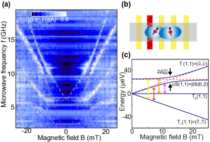
When we increase the interdot tunneling (Fig. 3(b)), the (1,1) states hybridize with S(0,2) resulting in level repulsion between spectral lines. In the absence of SOI, only states with the same spin can hybridize e.g. S(1,1) with S(0,2). SOI, however, also enables hybridization between the singlets and the triplets Schreiber2010 ; Fasth2007 ; Pfund2007 ; Danon2009a (Fig. 3; see also Fig. 4(e)). All observed transitions in Fig. 3(a) can be identified using a simple model which takes into account the hybridization between the (1,1) triplets and S(0,2) (see supp section S4). The four avoided crossings observed in Fig. 3(a) correspond to the same double dot spin-orbit gap between T-(1,1) and the singlet, as illustrated in Fig. 3(c). The quantitative comparison with the model allows us to estimate the spin-orbit length lSO = 230 ± 40 nm (see supp section S5).

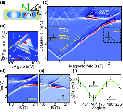
The observed singlet-triplet gap is highly anisotropic (Fig. 4). The gap is largest when is parallel to the nanowire axis : shrinks as the direction of is rotated in the sample plane (Fig. 4(b) and 4(c)). Finally for the gap disappears (Fig. 4(d)). For this orientation the resonance line corresponding to the T+(1,1) to singlet transition becomes straight indicating the absence of level repulsion between T-(1,1) and singlet. In addition, the visibility of the T+(1,1) T-(1,1) transition vanishes, suggesting that both T+(1,1) and T-(1,1) states are completely blocked for this field orientation.
The observed anisotropy of confirms the spin-orbit origin of the singlet-triplet level repulsion (see also supp section S3). The gap is expected to be proportional to Danon2009a ; Nowak2011 ; Stepanenko2011 . When the two fields are aligned, singlet and triplet states cannot mix and therefore the spin-orbit gap closes (Fig. 4(d)). From the observed anisotropy we conclude that points perpendicular to the nanowire and is parallel to the substrate plane (Figs. 4(i) and 4(a)).
The knowledge of orientation provides a substantial increase in the fidelity of the initialization and readout of spin-orbit qubits Nadj-Perge2010a . The fidelity is presently limited due to unwanted transitions from T+(1,1) and T-(1,1) to S(0,2) induced by SOI. When and are misaligned, T+(1,1) and T-(1,1) are coupled to S(0,2) (Fig. 4(e)) Danon2009a . The unwanted transitions are manifest in the d.c. current through the double dot at finite magnetic fields (Figs. 4(f), 4(g), 4(h)) Nadj-Perge2010 ; Pfund2007 . For an ideal readout and initialization no current flows after either T+(1,1) or T-(1,1) state is occupied. When is aligned with , T+(1,1) and T-(1,1) become decoupled from S(0,2) and d.c. current is expected to vanish. This dramatic suppression of d.c. current is observed for (Fig. 4(h)). Importantly, both and I show almost identical angle dependence further confirming that the singlet-triplet hybridization due to SOI is absent when || (Fig. 4(i)).
Given the direction of we can analyze the origin of the spin-orbit interaction in InSb nanowires. The field depends on the electron momentum . In a simple physical picture, during the interdot tunneling, the momentum is along the nanowire, which is grown in the [111] crystallographic direction. In zincblende InSb the spin-orbit interaction has two contributions, the bulk-inversion asymmetry term (BIA) and the structure-inversion asymmetry term (SIA). However, for || [111] the BIA term is expected to vanish Winkler2003 , and therefore the SIA contribution should dominate. The field due to SIA is orthogonal to both the momentum and the external electric field (Fig. 1(c)). The electric field is likely perpendicular to the substrate since the symmetry of confinement in the nanowire is broken by the substrate dielectric and voltages on the gates. Therefore the direction and in the substrate plane is consistent with the SIA spin-orbit interaction.
We compare the results obtained from EDSR spectroscopy with the spectrum of (0,2) states (Fig. 5(a)) Nilsson2009 ; Pfund2007 ; Fasth2007 . The SOI hybridization of S(0,2) and T+(0,2) states leads to a single dot spin-orbit gap . Since the energies of the (0,2) states are too large to be accessed with microwaves (ST 5 meV at B=0), we use the lowest energy T+(1,1) level as a probe of the (0,2) spectrum. By changing detuning we move T+(1,1) with respect to the (0, 2) levels. When T+(1,1) is aligned with either S(0,2) or T+(0,2), an increase in d.c. current is observed (Fig. 5(b)) Pfund2007a . The level repulsion between T+(0,2) and S(0,2) is observed at B 2T (Fig. 5(c)). The single dot gap is also strongly anisotropic reaching the smallest value for (Figs. 5(d), 5(e) and 5(f)). The spin-orbit length lSO = 310 ± 50 nm estimated from is in agreement with the value obtained using EDSR.

Recent proposals for experimental detection of Majorana bound states in hybrid nanowire-superconductor devices require wires with strong spin-orbit coupling Lutchyn2010 ; Oreg2010 . Besides InSb, indium arsenide (InAs) and p-type silicon/germanium (Si/Ge) nanowires kloeffel2011 are among most promising material systems for this purpose. Majorana states are expected to appear at the boundaries of the topological superconducting phase. The topological phase is predicted to occur if: (i) EZ > and (ii) Etop, > T. Here is the superconducting gap, Etop is the gap of the topological phase and T is the temperature. Due to large g-factors in InSb nanowires first requirement is satisfied at low magnetic fields even if large gap superconductors such as niobium are used ( 5K). This is a clear advantage since low magnetic fields are preferential in order not to suppress superconductivity. The size of the topological gap is determined by the bulk SOI splitting ESO = Streda2003 . Here is the Planck constant and is the effective electron mass ( is the electron mass). We can estimate ESO 0.5 K and Etop 3 K for the case of ballistic one-dimensional transport. While ESO is expected to be an order of magnitude larger for p-type Si/Ge wires kloeffel2011 the ESO 0.1-0.3 K is similar for InAs wurtzite nanowires supp (- for wurtzite InAs pryor2010 ). Note however that besides strength of SOI experimental details such as quality of semiconductor-superconductor interface as well as disorder may in the end determine the most promising material system. Finally we note that the anisotropy measurements (Fig. 4 and 5) suggest the orientation to be optimal for observing Majorana states since the maximum mixing of the SOI-split bands occurs for and the superconductivity is suppressed least when is in the substrate plane.
We would like to thank J. Danon, Y. Nazarov, M. Rudner, D. Loss, F. Hassler and J. van Tilburg for discussions and help. We acknowledge help with the measurement software from R. Heeres and P. de Groot. This work has been supported by ERC, NWO/FOM Netherlands Organization for Scientific Research and through the DARPA program QUEST.
References
- (1) Středa, P. and Šeba, P., Phys. Rev. Lett. 90, 256601 (2003).
- (2) Lutchyn, R. M., Sau, J. D., and Das Sarma, S., Phys. Rev. Lett. 105, 077001 (2010).
- (3) Oreg, Y., Refael, G., and von Oppen, F., Phys. Rev. Lett. 105, 177002 (2010).
- (4) Kitaev, A. Y., Phys. Usp. 44, 131 (2001).
- (5) Nilsson, H. A., Caroff, P., Thelander, C., Larsson, M., Wagner, J. B., Wernersson, L.-E., Samuelson, L., and Xu, H. Q., Nano Lett. 9, 3151 (2009).
- (6) Nilsson, H. A., Samuelsson, P., Caroff, P., and Xu, H. Q., Nano Lett. 12 228 (2012).
- (7) Schreiber, L. R., Braakman, F., Meunier, T., Calado, V., Danon, J., Taylor, J. M., Wegscheider, W., and Vandersypen, L. M. K., Nature Commun. 2, 556 (2011).
- (8) Pfund, A., Shorubalko, I., Ensslin, K., and Leturcq, R., Phys. Rev. B 76, 161308 (2007).
- (9) Fasth, C., Fuhrer, A., Samuelson, L., Golovach, V. N., and Loss, D., Phys. Rev. Lett. 98, 266801 (2007).
- (10) Nadj-Perge, S., Frolov, S. M., Bakkers, E. P. A. M., and Kouwenhoven, L. P., Nature 468, 1084 (2010).
- (11) Nowack, K. C., Koppens, F. H. L., Nazarov, Y. V., and Vandersypen, L. M. K., Science 318, 1430 (2007).
- (12) Takahashi, S., Deacon, R. S., Yoshida, K., Oiwa, A., Shibata, K., Hirakawa, K., Tokura, Y., and Tarucha, S., Phys. Rev. Lett. 104, 246801 (2010).
- (13) Kanai, Y., Deacon, R. S., Takahashi, S., Oiwa, A., Yoshida, K., Shibata, K., Hirakawa, K., Tokura, Y., and Tarucha, S., Nature Nanotech. 6, 511 (2011).
- (14) Golovach, V. N., Khaetskii, A., and Loss, D., Phys. Rev. B 77, 045328 (2008).
- (15) Nadj-Perge, S., Frolov, S. M., van Tilburg, J. W. W., Danon, J., Nazarov, Y. V., Algra, R., Bakkers, E. P. A. M., and Kouwenhoven, L. P., Phys. Rev. B 81, 201305(R) (2010).
- (16) Pioro-Ladriere, M., Obata, T., Tokura, Y., Shin, Y. S., Kubo, T., Yoshida, K., Taniyama, T., and Tarucha, S., Nature Phys. 4, 776 (2008).
- (17) Petta, J. R., Johnson, A. C., Taylor, J. M., Laird, E. A., Yacoby, A., Lukin, M. D., Marcus, C. M., Hanson, M. P., and Gossard, A. C., Science 309, 2180 (2005).
- (18) Koppens, F. H. L., Buizert, C., Tielrooij, K. J., Vink, I. T., Nowack, K. C., Meunier, T., Kouwenhoven, L. P., and Vandersypen, L. M. K., Nature 442, 766 (2006).
- (19) Winkler, R., Spin-Orbit Coupling Effects in Two-Dimensional Electron and Hole Systems. Springer, Berlin, (2003).
- (20) Flindt, C., Sorensen, A. S., and Flensberg, K., Phys. Rev. Lett. 97, 240501 (2006).
- (21) Ono, K., Austing, D. G., Tokura, Y., and Tarucha, S., Science 297, 1313 (2002).
- (22) Koppens, F. H. L., Folk, J. A., Elzerman, J. M., Hanson, R., van Beveren, L. H. W., Vink, I. T., Tranitz, H. P., Wegscheider, W., Kouwenhoven, L. P., and Vandersypen, L. M. K., Science 309, 1346 (2005).
- (23) Danon, J. and Nazarov, Y. V., Phys. Rev. B 80, 041301 (2009).
- (24) Supplementary Material accompanies this paper. It can be downloaded at http://link.aps.org/supplemental/ 10.1103/PhysRevLett.108.166801
- (25) Bell, R. L., Phys. Rev. Lett. 9, 52 (1962).
- (26) Golovach, V. N., Borhani, M., and Loss, D., Phys. Rev. B 74, 165319 (2006).
- (27) Laird, E. A., Barthel, C., Rashba, E. I., Marcus, C. M., Hanson, M. P., and Gossard, A. C., Phys. Rev. Lett. 99, 246601 (2007).
- (28) Pryor, C. E. and Flatté, M. E., Phys. Rev. Lett. 96, 026804 (2006).
- (29) Schroer, M. D., Petersson, K. D., Jung, M., and Petta, J. R., Phys. Rev. Lett. 107, 176811 (2011).
- (30) Pfund, A., Shorubalko, I., Ensslin, K., and Leturcq, R., Phys. Rev. Lett. 99, 036801 (2007).
- (31) Nowak, M. P., Szafran, B., Peeters, F. M., Partoens, B., and Pasek, W. J., Phys. Rev. B 83, 245324 (2011).
- (32) Stepanenko, D., Rudner, M., Halperin, B. I., and Loss, D., Phys. Rev. B 85, 075416 (2012).
- (33) Kloeffel, C., Trif, M., and Loss, D. Phys. Rev. B 84, 195314 (2011).
- (34) De, A., and Pryor, C. E., Phys. Rev. B 81, 155210 (2010).